


RX-7010RBK
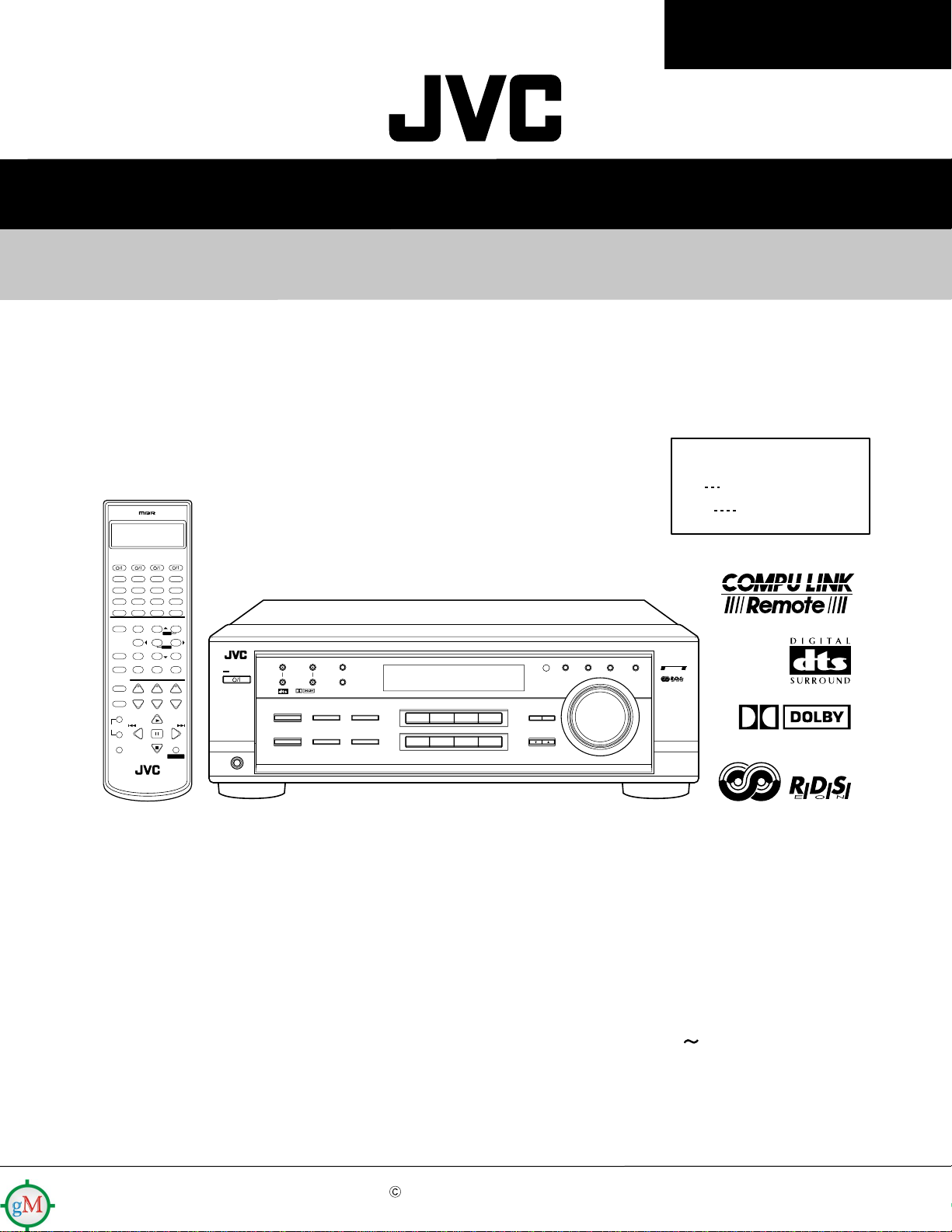
RX-7010RBK/RX-7012RSL
SERVICE MANUAL
AUDIO/VIDEO CONTROL RECEIVER
RX-7010RBK
RX-7012RSL
Area Suffix
CATV/DBS VCR TV AUDIO
DVD MUILTIDVD
CD
TAPE/CDR
TV/DBS VCR PHONO
TREBLE
BASS
++−−
ANALOG/DIGITAL
DSP
SURROUND
MODE INPUTON/OFF
+ CENTER –
BASS BOOST EFFECT
231
MENU
TEST + REAR•L –
564
ENTER
– REAR•R +
SOUND
897/P
– SUB WOOFER +
MUTING
0
RETURN FM MODE 100
CATV/DBS
CONTROL
CONTROL
+−+−+
CH TV VOL
TV/VIDEO
PLAY
+
/REW FF/
PAUS E
TUNING
−
REC
PTY SEARCH
PTY–
PAUSE
STOP
Y
DISPLA
RM-SRX7010R
A/V CONTROL RECEIVER
FM/AM
SLEEP
VOLUME
PTY+
CONTROL
E
EN
FM/AM TUNING
DIGITAL
SURROUND
SURROUND ON/OFF
DSP MODE
FM/AM PRESET FM MODE
DIGITAL
ANALOG/DIGITAL
INPUT ATT
MEMORY
INPUT
BASS BOOST
SPEAKERS ON/OFF
12
+1010
+
STANDBY
STANDBY/ON
−
PHONES
AUDIO/VIDEO CONTROL RECEIVER
DVD VCR
DVD MULTI
PHONO
CD TAPE/CDR
SOURCE NAME
TV SOUND/DBS
SOURCE NAME
FM/AM
EON PTY SEARCH TA/NEWS/INFO DISPLAY MODE
ADJUST
SETTING
CONTROL
DOWN UP
MASTER VOLUME
COMPULINK
Remote
Continental Europe
Northern Europe
DIGITAL
As for RX-7012RSL the body is silver color
Contents
Safety precautions --------------------------------------------------------1-2
Disassembly method -----------------------------------------------------1-3
Adjustment method -------------------------------------------------------1-8
Description of major ICs -------------------------------------------------1-9 19
COPYRIGHT 2001 VICTOR COMPANY OF JAPAN, LTD.
No.20938
Apr. 2001
http://getMANUAL.com
RX-7010RBK/RX-7012RSL
1. This design of this product contains special hardware and many circuits and components specially for safety
purposes. For continued protection, no changes should be made to the original design unless authorized in
writing by the manufacturer. Replacement parts must be identical to those used in the original circuits. Services
should be performed by qualified personnel only.
2. Alterations of the design or circuitry of the product should not be made. Any design alterations of the product
should not be made. Any design alterations or additions will void the manufacturer`s warranty and will further
relieve the manufacture of responsibility for personal injury or property damage resulting therefrom.
3. Many electrical and mechanical parts in the products have special safety-related characteristics. These
characteristics are often not evident from visual inspection nor can the protection afforded by them necessarily
be obtained by using replacement components rated for higher voltage, wattage, etc. Replacement parts which
have these special safety characteristics are identified in the Parts List of Service Manual. Electrical
components having such features are identified by shading on the schematics and by ( ) on the Parts List in
the Service Manual. The use of a substitute replacement which does not have the same safety characteristics
as the recommended replacement parts shown in the Parts List of Service Manual may create shock, fire, or
other hazards.
4. The leads in the products are routed and dressed with ties, clamps, tubings, barriers and the like to be
separated from live parts, high temperature parts, moving parts and/or sharp edges for the prevention of
electric shock and fire hazard. When service is required, the original lead routing and dress should be
observed, and it should be confirmed that they have been returned to normal, after re-assembling.
5. Leakage currnet check (Electrical shock hazard testing)
After re-assembling the product, always perform an isolation check on the exposed metal parts of the product
(antenna terminals, knobs, metal cabinet, screw heads, headphone jack, control shafts, etc.) to be sure the
product is safe to operate without danger of electrical shock.
Do not use a line isolation transformer during this check.
Plug the AC line cord directly into the AC outlet. Using a "Leakage Current Tester", measure the leakage
current from each exposed metal parts of the cabinet, particularly any exposed metal part having a return
path to the chassis, to a known good earth ground. Any leakage current must not exceed 0.5mA AC (r.m.s.).
Alternate check method
Plug the AC line cord directly into the AC outlet. Use an AC voltmeter having, 1,000 ohms per volt or more
sensitivity in the following manner. Connect a 1,500 10W resistor paralleled by a 0.15 F AC-type capacitor
between an exposed metal part and a known good earth ground.
Measure the AC voltage across the resistor with the AC
voltmeter.
Move the resistor connection to eachexposed metal part,
particularly any exposed metal part having a return path to
the chassis, and meausre the AC voltage across the resistor.
Now, reverse the plug in the AC outlet and repeat each
measurement. voltage measured Any must not exceed 0.75 V
AC (r.m.s.). This corresponds to 0.5 mA AC (r.m.s.).
0.15 F AC TYPE
1500 10W
Good earth ground
AC VOLTMETER
(Having 1000
ohms/volts,
or more sensitivity)
Place this
probe on
each exposed
metal part.
!
1. This equipment has been designed and manufactured to meet international safety standards.
2. It is the legal responsibility of the repairer to ensure that these safety standards are maintained.
3. Repairs must be made in accordance with the relevant safety standards.
4. It is essential that safety critical components are replaced by approved parts.
5. If mains voltage selector is provided, check setting for local voltage.
Burrs formed during molding may
be left over on some parts of the
chassis. Therefore, pay attention to
such burrs in the case of
preforming repair of this system.
In regard with component parts appearing on the silk-screen printed side (parts side) of the PWB diagrams, the
parts that are printed over with black such as the resistor ( ), diode ( ) and ICP ( ) or identified by the " "
mark nearby are critical for safety.
When replacing them, be sure to use the parts of the same type and rating as specified by the manufacturer.
(Except the JC version)
1-2
RX-7010RBK/RX-7012RSL
Disassembly method
Removing the top cover (See Fig.1)
1.
Remove the four screws A attaching the top cover
on both sides of the body.
2.
Remove the three screws B on the back of the body.
3.
Remove the top cover from behind in the direction of
the arrow while pulling both sides outward.
Removing the front panel assembly
(See Fig.2 and 3)
Prior to performing the following procedure, remove
the top cover.
1.
Disconnect the card wire from connector CN402 on
the audio board and CN201 on the power supply
board in the front panel assembly.
2.
Cut off the tie band fixing the harness.
Tie band
Main
board
CN402
Top cover
A
2
A
B
2
C
Fig.1
Front panel assembly
C
CN201
Power supply
board
3.
Remove the three screws C attaching the front
panel assembly.
4.
Remove the four screws D attaching the front panel
assembly on the bottom of the body. Detach the front
panel assembly toward the front.
Removing the rear panel (See Fig.4)
Prior to performing the following procedure, remove
the top cover.
1.
Remove the power cord stopper from the rear panel
by moving it in the direction of the arrow.
2.
Remove the twenty seven screws E attaching the
each boards to the rear panel on the back of the
body.
3.
Remove the four screws F attaching the rear panel
on the back of the body.
Audio board
E
E
F
D
E
E
Rear panel
Fig.2
Front panel assembly
Fig.3
E
E
F
D
Cord stopper
E
F
F
Fig.4
1-3
RX-7010RBK/RX-7012RSL
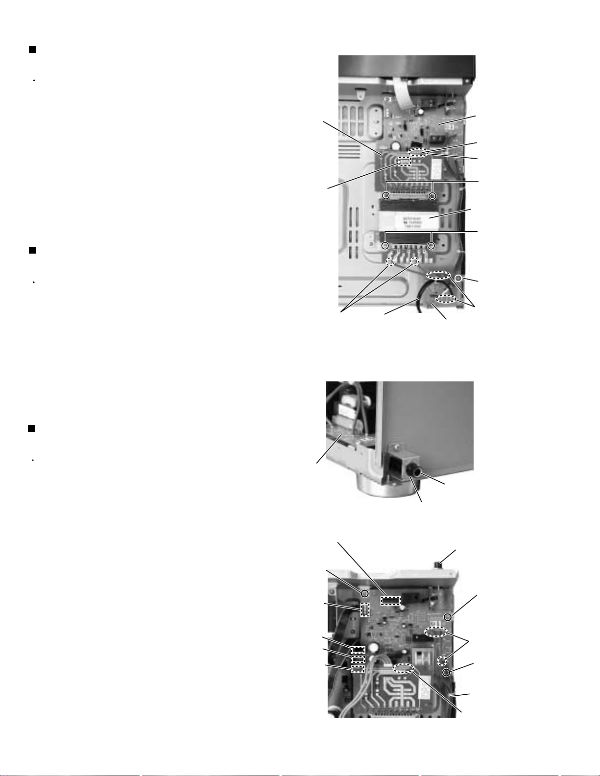
Removing each board connected to the
rear side of the audio board
(See Fig.5 to 8)
Prior to performing the following procedure, remove
the top cover and the rear panel.
1.
Cut off the tie band fixing the harness.
Audio
board
Tie band
Tie band
CN411
CN412
2.
Disconnect the DSP board from connector CN481 on
the audio board.
3.
Disconnect the audio input board, DVD board Video
board and the S video board from connector CN421,
CN431,CN441 and CN461 on the audio board.
4.
Disconnect the tuner board from connector CN411
and CN412 on the audio board.
DSP
board
CN481
CN421
Audio
input
board
CN431
DVD
board
CN481
Video
board
DSP board
CN441
S Video
board
Fig.5
Tie band
Tuner
board
CN461
CN421
Tie band
CN431
Fig.8
CN441
CN461
Tuner
board
CN411
CN412
Audio
input
board
CN421
Fig.6
DVD
board
CN431
Fig.7
Video
board
CN441
S Video
board
CN461
1-4

Removing the audio board (See Fig.9)
Prior to performing the following procedure, remove
the top cover and the rear panel.
1.
Disconnect the card wire from connector CN402 on
the audio board.
2.
Disconnect the relay board from the audio board and
the power supply board. (CN291,CN491)
3.
Disconnect the harness from connector CN473,
CN471, CN472, CN403 and CN385.
4.
Remove the three screws G attaching the audio
board assembly.
5.
Remove the screw H attaching the audio board
assembly.
CN473
G
CN402
G
Audio board
CN471
CN472
CN403
CN385
RX-7010RBK/RX-7012RSL
Relay board
power
supply
board
CN291
Power
transformer
G
Fig.9
I
CN491
CN241
Power / Fuse
H
board
Removing the main board (See Fig.10)
Prior to performing the following procedure, remove
the top cover, the rear panel and audio board.
1.
Disconnect the harness from connector CN241 and
CN203 on the power supply board respectively.
2.
Remove the four screws I and the two screws J
attaching the main board.
3.
In case where the sub board is installed,detach it
after removing the connectors CN208,CN209 and
CN210 as well as the screw J'.
Removing the Heat sink
(See Fig.11 to 12)
1.
Remove the ten screws K and four screws L
attaching the heat sink.
2.
Remove the two screws L' attaching the heat sink
from the rear side of main board.
Main
board
I
J
J
CN203
I
I
J'
Fig.10
CN208
CN209
CN210
L'
Heat sink
L
K
Fig.11
K
K
L'
L
Main board
rear side
Fig.12
1-5
RX-7010RBK/RX-7012RSL
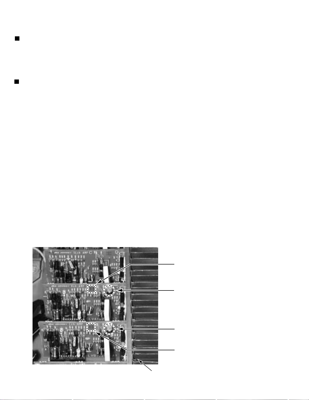
Removing the power transformer
(See Fig.13)
Prior to performing the following procedures, remove
the top cover.
1.
Unsolder the two harnesses connected to the power
transformer.
2.
Disconnect the harness from connector CN251 and
unsolder the harnesses connected to FW201 on the
power transformer board.
3.
Remove the four screws M attaching the power
transformer.
Removing the power / fuse board
(See Fig.13)
Prior to performing the following procedure, remove
the top cover and the rear panel.
1.
Remove the screw N attaching the power / fuse
board.
Power
transformer
board
CN251
Solder
Power cord
Power
supply
board
FW201
Solder
M
Power
transformer
M
N
Solder
Power / fuse board
2.
Unsolder the power cord and other harnesses
connected to the power / fuse board.
Removing the power supply board
(See Fig.14 and 15)
Prior to performing the following procedure, remove
the top cover and the front panel.
1.
Remove the one nut attaching the headphone jack of
the power supply board on the front side of the body.
2.
Disconnect the harness connected to connector
CN241,CN201,CN203 and CN291 on the power
transformer board (If necessary, cut off the band
fixing the harness on the side of the base chassis).
3.
Remove the three screws O attaching the power
supply board and pull out the power supply board
from the front bracket backward.
Power
supply
board
CN201
O
CN241
Fig.13
Headphone jack
Nut
Fig.14
Headphone jack
O
4.
Unsolder the three harnesses connected to the
power supply board.
1-6
CN203
CN291
Hook
Solder
O
Tie band
Solder
Fig.15

RX-7010RBK/RX-7012RSL
Removing the system control board /
power switch board (See Fig.16 to 18)
Prior to performing the following procedure, remove
the top cover and the front panel assembly.
1.
Pull out the volume knob on the front side of the front
panel and remove the nut attaching the system
control board.
2.
Remove the two screws P attaching the power
switch board.
3.
Disconnect the harness from connector CN714 on
the power switch board.
4.
Remove the six screws Q attaching the system
control board on the back of the front panel.
5.
On the back of the front panel, release the eight
joints by pushing the joint tabs inward.
Remove the operation switch panel toward the front.
6.
Release the two hook attaching the system control
board.
Operation switch panel
Fig.16
Q
Joint
Joint
Q
Nut
Joint
Front panel assembly
Volume knob
Power switch
board
Joint
P
Joint
Joint
Hook
Joint
Fig.17
System control board
Fig.18
Hook
Joint
CN714
1-7
RX-7010RBK/RX-7012RSL
Adjustment method
Tuner section
1.Tuner range
FM 87.5MHz~108.0MHz
AM (MW) 522kHz~1629kHz
(LW) 144kHz~ 288kHz
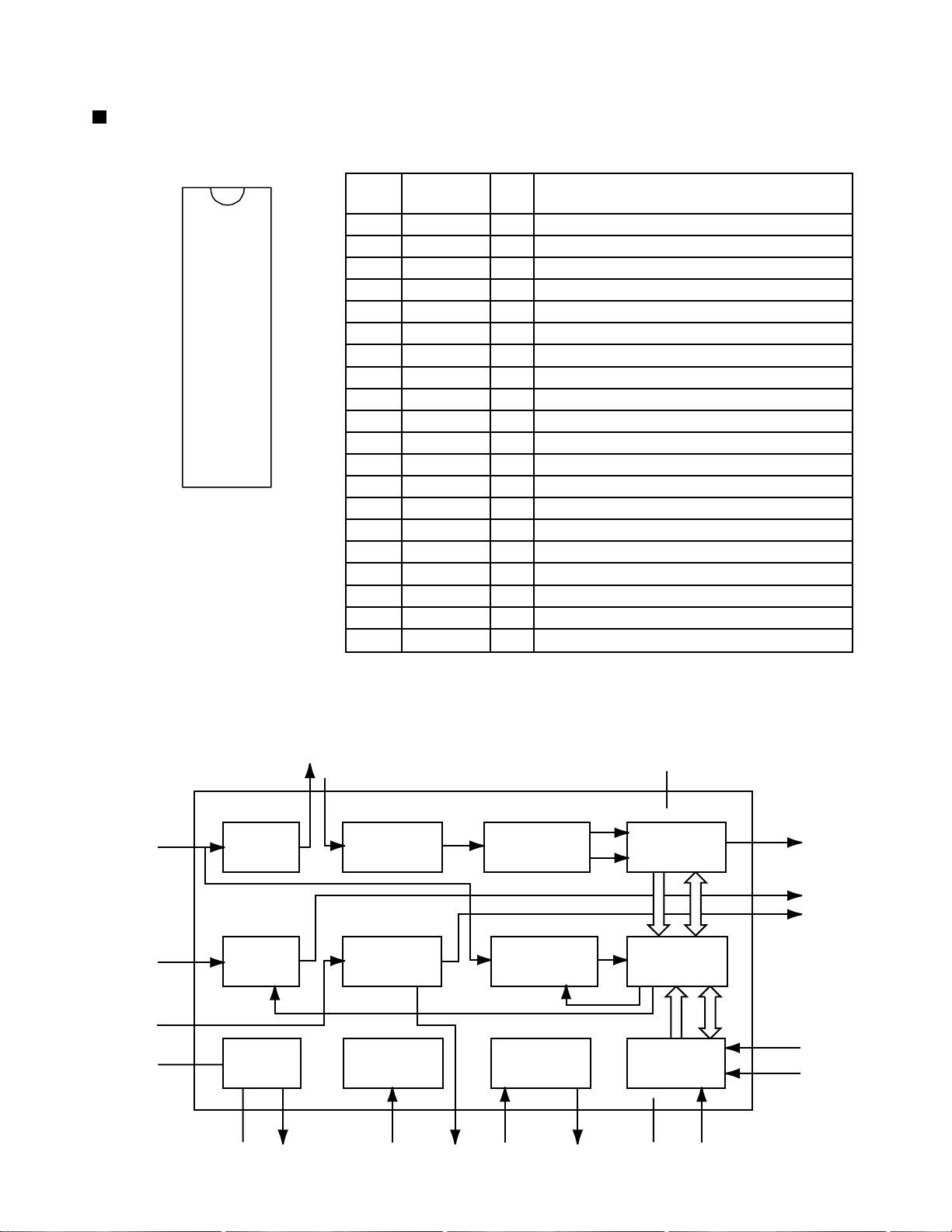
Power amplifier section
Adjustment of idling current
Measurement location TP301(Lch) , TP302(Rch)
Adjustment part VR301(Lch) , VR302(Rch)
Attention
This adjustment does not obtain a correct adjustment value immediately after the amplifier is
used (state that an internal temperature has risen).
Please adjust immediately after using the amplifier after turning off the power supply of the
amplifier and falling an internal temperature.
<Adjustment method>
1.Set the volume control to minimum during this adjustment.(No signal & No load)
2.Set the surround mode OFF.
2.Turn VR301 and VR302 fully counterclockwise to warm up before adjustment.
If the heat sink is already warm from previous use the correct adjustment can not be made.
3.For L-ch,connect a DC voltmeter between TP301's B216 and B217 (Lch)
And,connect it between TP302's B218 and B219(Rch).
4.30 minutes later after power on, adjust VR301 for L-ch, or VR302 for R-ch so that the DC voltmeter
value has 1mV~10mV.
* It is not abnormal though the idling current might not become 0mA even if it is finished to turn variable
resistance (VR301,VR302) in the direction of counterclockwise.
TP302(Rch)
VR302 (Rch)
1-8
VR301 (Lch)
TP301(Lch)
Heat sink
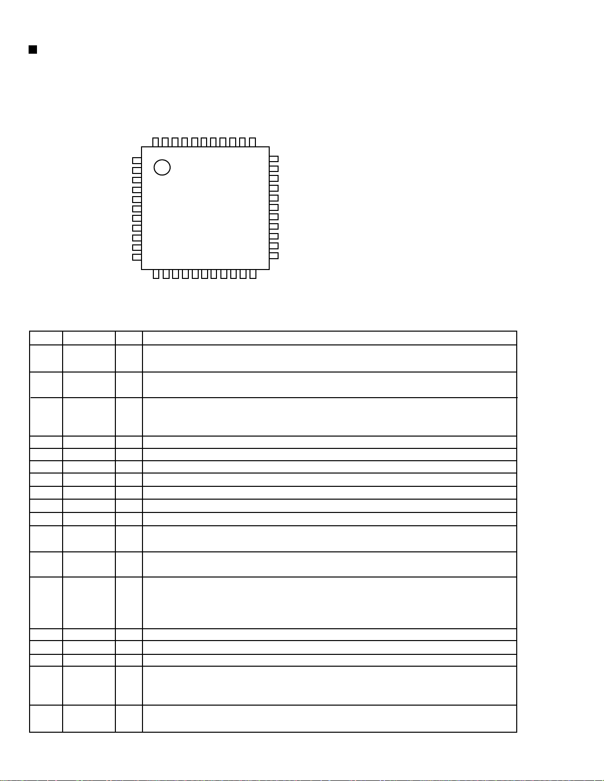
Description of major ICs
SAA6588 (IC191) : RDS detector
RX-7010RBK/RX-7012RSL
1.Terminal Layout
NC
GND
SDA
SCL
1
2
3
4
5
6
7
8
9
10
MRO
OSCO
OSCI
VSSD
VDDD
DAVN
20
19
18
17
16
15
14
13
12
11
NC
CIN
SCOUT
Vref
MPX
VSSA
VDDA
NC
GND
NC
2.Pin Function
Pin
No.
1
2
3
4
5
6
7
8
9
10
11
12
13
14
15
16
17
18
19
20
MRO
NC
GND
OSCO
OSCI
VSSD
VDDD
DAVN
SDA
SCL
NC
GND
NC
VDDA
VSSA
MPX
Vref
SCOUT
CIN
NC
FunctionI/OSymbol
O
Multi-path rectifier output
-
Non connect
I
Test control input pin
O
Oscillator output
I
Oscillator input
-
Digital ground (0V)
-
Digital power supply (5V)
O
Data available output (active LOW)
I/O
IC-bus serial data I/O
I
IC-bus serial clock input
-
Non connect
-
Connect to ground
-
Non connect
-
Analog power supply (5V)
Connect to ground
-
Multiplex input signal
I
Reference voltage output
O
Band-pass filter output
O
Comparator output
O
Level input
I
3.Block Diagram
16
MPX
13
AFIN
LVIN
20
VDDA
14
8th ORDER
BAND-PASS
DETECTOR
AND RESET
VSSA
SCOUT
57 kHz
PAUSE
POWER
SUPPLY
15
18
17
Vref
19
CLOCK
COMPARATOR
MULTI-PATH
DETECTOR
TEST
CONTROL
3
TCON
RDS/RDBS
DEMODULATOR
SIGNAL QUALITY
DETECTOR
OSCILLATOR
AND CLOCK
1
MRO
OSCI OSCO
VDDDCIN
7
DAVN
12
MAD
11
10
8
2
9
PSWN
MPTH
SDA
SCL
RDS/RDBS
DECODER
INTERFACE
REGISTER
IC-BUS SLAVE
TRANSCEIVER
5
4
6
VSSD
1-9
RX-7010RBK/RX-7012RSL
AK4527B (IC601) : A/D,D/A converter
1.Pin layout
LOOP1
LOOP0/SDA/CDTI
DIF1/SCL/CCLK
DIF0/CSN
P/S
MCLK
DZF1
AVSS
AVDD
VREFH
VCOM
SDOS
I2C
SMUTE
BICK
LRCK
SDTI1
SDTI2
SDTI3
SDTO
DAUX
DFS
2. Pin function (1/2)
No.
1
2
3
4
5
6
7
8
9
10
11
12
13
14
15
16
17
18
Pin name
SDOS
I2C
SMUTE
BICK
LRCK
SDTI1
SDTI2
SDTI3
SDTO
DAUX
DFS
NC
DZEF
TVDD
DVDD
DVSS
PDN
TST
4443424140393837363534
1
2
3
4
5
6
7
8
9
10
11
I/O
I
SDTO Source Select Pin (Note 1)
AK4527BVQ
Top View
1213141516171819202122
NC
DZFE
TVDD
DVDD
DVSS
PDN
TSTNCADIF
Function
CAD1
CAD0
33
32
31
30
29
28
27
26
25
24
23
DZF2/OVF
RIN+
RINLIN+
LINROUT1
LOUT1
ROUT2
LOUT2
ROUT3
LOUT3
"L" : Internal ADC output, "H" : DAUX input
I
Control Mode Select Pin
"L" : 3-wire Serial, "H" : I
I
Soft Mute Pin (Note 1)
2
C Bus
When this pin goes to "H", soft mute cycle is initialized.
When returning to "L", the output mute releases.
I
Audio Serial Data Clock Pin
I/O
Input Channel Clock Pin
I
DAC1 Audio Serial Data Input Pin
I
DAC2 Audio Serial Data Input Pin
I
DAC3 Audio Serial Data Input Pin
O
Audio Serial Data Output Pin
I
Sub Audio Serial Data Input Pin
I
Double Speed Sampling Mode Pin (Note 1)
"L" : Normal Speed, "H" : Double Speed
-
No Connect
No internal bonding.
I
Zero Input Detect Enable Pin
"L" : mode 7 (disable) at parallel mode,
zero detect mode is selectable by DZFM2-0 bits at serial mode.
"H" : mode 0 (DZF is AND of all six channels)
-
Output Buffer Power supply Pin, 2.7V~5.5V
-
Digital Power Supply Pin, 4.5V~5.5V
-
De-emphasis Pin, 0V
I
Power-Down & Reset Pin
When "L", the AK4527B is powered-down and the control registers are reset to default
state. If the state of P/S or CAD0-1 changes, then the AK4527B must be reset by PDN.
I
Test Pin
This pin should be connected to DVSS.
AK4527(1/2)
1-10
RX-7010RBK/RX-7012RSL
g
Pin function (2/2)
No.
Pin name
19
NC
20
ADIF
21
CAD1
22
CAD0
23
LOUT3
24
ROUT3
25
LOUT2
26
ROUT2
27
LOUT1
28
ROUT1
29
LIN-
30
LIN+
31
RIN-
32
RIN+
33
DZF2
OVF
34
VCOM
35
VREFH
36
AVDD
37
AVSS
38
DZF1
39
MCLK
40
P/S
41
DIF0
CSN
42
DIF1
SCL/CCLK
43
LOOP0
SAD/CDTI
44
LOOP1
I/O
No Connect
No internal bonding.
Analog Input Format Select Pin
I
"H" : Full-differential input, "L" : Single-ended input
Chip Address 1 Pin
I
Chip Address 0 Pin
I
DAC3 Lch Analog Output Pin
O
DAC3 Rch Analog Output Pin
O
DAC2 Lch Analog Output Pin
O
DAC2 Rch Analog Output Pin
O
DAC1 Lch Analog Output Pin
O
DAC1 Rch Analog Output Pin
O
Lch Analog Negative Input Pin
I
Lch Analog Positive Input Pin
I
Rch Analog Negative Input Pin
I
Rch Analog Positive Input Pin
I
Zero Input Detect 2 Pin (Note 2)
O
When the input data of the group 1 follow total 8192LRCK cycles with "0" input data,
this pin goes to "H".
Analog Input Overflow Detect Pin (Note 3)
O
This pin goes to "H" if the analog input of Lch or Rch is overflows.
Common Voltage Output Pin,AVDD/2
O
Large external capacitor around 2.2uF is used to reduce power-supply noise.
Positive Voltage Reference Input Pin,AVDD
I
Analog Power Supply Pin,4.5V~5.5V
Analog Ground Pin,0V
Zero Input Detect 1 Pin (Note 2)
O
When the input data of the group 1 follow total 8192 LRCK cycles with "0" input data,
this pin goes to "H".
Master Clock Input Pin
I
Parallel / Serial Select Pin
I
"L" : Serial control mode, "H" : Parallel control mode
Audio Data Interface Format 0 Pin in parallel mode
I
Chip select pin in 3-wire serial control mode
I
This pin should be connected to DVDD at I2C bus control mode
Audio Data Interface Format 1 Pin in parallel mode
I
Control Data Clock Pin in serial control mode
I
I2C = "L" : CCLK(3-wire Serial), I2C = "H" : SCL(I2CBus)
Loopback Mode 0 Pin in parallel control mode
I
Enables digital loop-back from ADC to 3 DACs.
Control Data Input Pin in serial control mode
I/O
I2C = "L" : CDTI(3-wire Serial), I2C = "H" : SDA(I2CBus)
Loopback Mode 1 Pin (Note 1)
I
Enable all 3 DAC channels to be input from SDTII.
Function
AK4527(1/2)
Notes : 1. SDOS, SMUTE, DFS, and LOOP1 pins are ORed with register data if P/S = "L".
2. The group 1 and 2 can be selected by DZFM2-0 bit if P/S = "L" and DZFME = "L".
3. This pin becomes OVF pin if OVFE bit is set to "1" at serial control mode.
4. All input pins should not be left floatin
.
1-11
RX-7010RBK/RX-7012RSL
TC9164AN (IC402) : Analog switch
1.Function
Switch to On/Off of S1 to S8 by control of LSI.
2.Terminal Lay out & Block Diagram
TC9164AN
VSS
L-S1
S-2
S-3
S-4
COM-1
S-5
S-6
COM-2
S-7
S-8
COM3
GND
ST
1
2
3
4
SHIFT
5
RESISTOR
6
7
8
9
10
11
12
13
14
&
LATCH
SHIFT RESISTOR
SHIFT
RESISTOR
&
LATCH
28
27
26
25
24
23
22
21
20
19
18
17
16
15
VDD
R-S1
S-2
S-3
S-4
COM-1
S-5
S-6
COM-2
S-7
S-8
COM3
DATA
CK
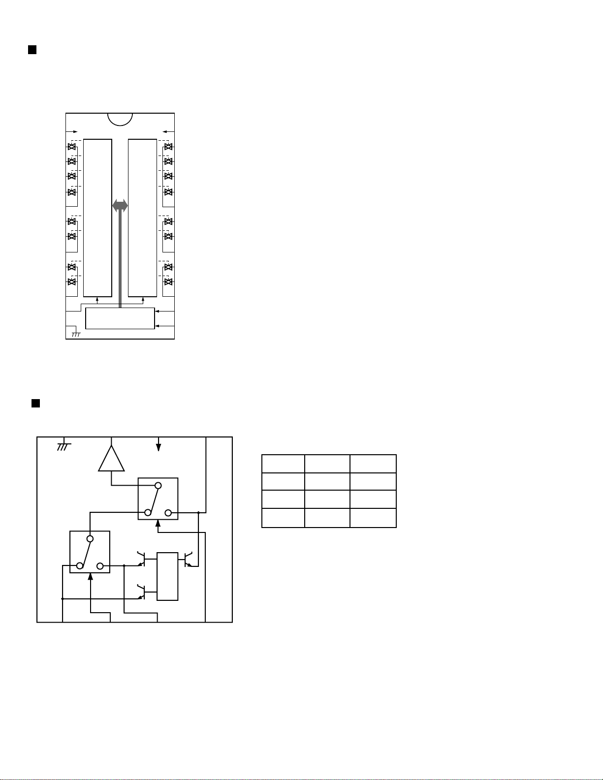
NJM2246D (IC501,IC551,IC552) : Video switch
GND
8
Vout
7
V+
6
5
Vin3
1
Vin1
6dB
AMP.
2
CTL1
3
Vin2
BIAS
4
CTL2
Control input - output signal
CTL 1
L
H
L/H
CTL 2
L
L
H
Output
VIN 1
VIN 2
VIN 3
1-12
W24L010AJ-12 (IC641) : CMOS SRAM
RX-7010RBK/RX-7012RSL
Block diagram
A16
A14
A12
A4
A3
A2
A7
A6
A5
A9
I/O 1
I/O8
WE
CS1
CS2
R
O
W
D
E
C
O
D
E
R
DATA
CNTRL.
CLK
GEN.
PRECHARGE CKT.CLK GEN.
CORE CELL ARRAY
7024 ROWS
728x8 COLUMN5
I/O CKT
COLUMN DECODER
A15 A13 A8 A1 A0 A11 A10
Pin layout
NC
A16
A14
A12
A7
A6
A5
A4
A3
A2
A1
A0
I/O1
I/O2
I/O3
Vss
1
2
3
4
5
6
7
8
9
10
11
12
13
14
15
16
32
31
30
29
28
27
26
25
24
23
22
21
20
19
18
17
VDD
A15
CS2
WE
A13
A8
A9
A11
OE
A10
CS2
I/O8
I/O7
I/O6
I/O5
I/O4
OE
PQ3DZ53 (IC681) : Regulator IC
DC INPUT(Vin)
1
CUSTOM IC
5
GND
RN5RZ33BA (IC683) : Voltage regurator
2
VDD
-
+
3
DC OUTPUT(Vo)
ON/OFF CONTROL(Vc)
2
VOUT
3
CE
Vref
GND
Current Limit
5
1
1-13
RX-7010RBK/RX-7012RSL
M62446FP (IC428) : 6CH master volume
1.Block Diagram
OUT4
OUT3
OUT2
OUT1
AVDD
SWIN
GNDS
SRin
SLin
GNDC
Cin
GNDR
Rin
GNDL
Lin
BYPASSR
BYPASSL
LTRE
LBASS3
LBASS2
LBASS1
10
11
12
13
14
15
16
17
18
19
20
21
1
2
3
4
5
6
7
8
9
OUTPUT
PORT
tone
volume
volume
volume
volume
volume
volume
MCU
I/F
tone
42
41
40
39
38
37
36
35
34
33
32
31
30
29
28
27
26
25
24
23
22
DVDD
CLK
D ATA
LATCH
DGND
AGND
SWout
SRout
SLout
Cout
Rout
Lout
AVSS
CL1
CL2
CR1
CR2
RTRE
RBASS3
RBASS2
RBASS1
1-14

2.Pin Function
RX-7010RBK/RX-7012RSL
Pin No.
1
2
3
4
5
6
7
8
9
10
11
12
13
14
15
16,17
18
19~21
22
23,24
25
26
27
28
29
30
31
32
33
34
35
36
37
38
39
40
41
42
Symbol I/O Descriptions
SURROUND
BASS BOOST
INPUT-ATT
MUTING
AVDD
SWIN
A.GND
RR IN
RL IN
A.GND
C IN
A.GND
R IN
A.GND
L IN
BYPASSR,L
LTRE
LBASS3~1
CR2
RBASS2,4
RTRE
RBASS1
CR1
CL2
CL1
AVSS
L OUT
R OUT
C OUT
RL OUT
RR OUT
SW OUT
A.GND
D.GND
VOL STB
VOL DATA
VOL CLK
DVDD
O
O
O
O
I
I
I
I
I
I
-
-
-
O
-
-
I
O
I
O
O
O
O
O
O
-
-
I
I
I
-
SURROUND control terminal
BASS BOOST control terminal
Input attenuator control terminal
MUTING control terminal
Analog positive power supply terminal
SUB Woofer volume signal input terminal
Analog ground terminal
R ch volume signal input terminal for rear speaker
L ch volume signal input terminal for rear speaker
Analog ground terminal
Center volume signal input terminal
Analog ground terminal
R ch volume signal input terminal
Analog ground terminal
L ch volume signal input terminal
Non connect
Frequency adjustment terminal tone/treble
Frequency adjustment terminal tone/bass
Tone output terminal
Frequency adjustment terminal tone/bass
Frequency adjustment terminal tone/treble
Frequency adjustment terminal tone/bass
L/R volume input terminal
Tone output terminal
L/R volume input terminal
Analog negative power supply terminal
L ch output
R ch output
Center volume signal output terminal
L ch volume signal output terminal for rear speaker
R ch volume signal output terminal for rear speaker
SUB Woofer volume signal output terminal
Analog ground terminal
Digital ground terminal
Latch input terminal
Volume data input terminal
Clock input terminal for data transfer
Digital power supply terminal
1-15
RX-7010RBK/RX-7012RSL
MN101C35DHK1 (IC701) : System controller
100 76
1
75
Pin function (1/2)
Pin No.
1
2
TXD/SB00/P00
RXD/SBI0/P01
3
4
5
6
7
BUZZER/P06
8
9,10
11
12
13
14
15
16
17
18
19
20
21
22
23
24
25
26
27
RNOUT/TM0I0/P10
28
29
30
31
32
33
34
SENS/IRQ1/P21
35
36
37
38
39
40
25
Symbol
SBT0/P02
SB01/P03
SBI1/P04
SBT1/P05
VDD
OSC1,2
VSS
XI
X0
MMOD
VREFAN0/PA0
AN1/PA1
AN2/PA2
AN3/PA3
AN4/PA4
AN5/PA5
AN5/PA5
AN5/PA5
VREF+
P07
RST /P27
TM1I0/P11
TM2I0/P12
TM3I0/P13
TM4I0/P14
P15
IRQ0/P20
IRQ2/P22
IRQ3/P23
IRQ4/P24
P25
SB02/P30
SBI2/P31
26 50
51
I/O
I
I
I/O
O
O
I
I
-
I/O
I
O
I
I
I
I
I
I
I
I
I
I
I
O
I
O
I
O
I/O
I
I
I
I
I
I
O
I
Function
VOL.JOG IN_1
VOL.JOG IN_2
DATA (PLL)
CLK (PLL)
CE (PLL)
VIDEO S/C DVD
VIDEO S/C VCR
Power supply +5V
OSC (8MHz)
GND
GND
OPEN
GND
GND
KEY INPUT 1 (7KEY)
KEY INPUT 2 (7KEY)
KEY INPUT 3 (7KEY)
KEY INPUT 4 (7KEY)
KEY INPUT 5 (7KEY)
INH IN
CHIP SELECT 1
CHIP SELECT 2
Power supply +5V
VIDEO S/C DBS
RESET INPUT
RDS CLK OUT (RDS)
DCS INPUT
DCS OUTPUT
AVLINK VCR IN
AVLINK VCR OUT
RDS DATA (RDS)
PROTECTOR IN
REMOCON INPUT
TUNED IN (TUNER)
STEREO IN (TUNER)
RDS DAVN (RDS)
SELF CHECK INPUT
COMMAND (DSP)
STATUS (DSP)
1-16
Pin function (2/2)
RX-7010RBK/RX-7012RSL
Pin No.
41
42
43
44
45
46
47
48
49 64
65 80
81
82
83
84
85
86
87
88
89
90
91
92
93
94
95
96
97
98
99
100
Symbol
SBT2/P32
P50
P51
P52
P53
P54
DGT17/P67
DGT16/P66
G16 G1
P87 P90
SEG24/PC2
SEG25/PC1
SEG26/PC0
SEG27/PB7
SEG28/PB6
SEG29/PB5
SEG30/PB4
SEG31/PB3
SEG32/PB2
SEG33/PB1
SEG34/PB0
SEG35/PD7
SEG36/PD6
SEG37/PD5
SEG38/PD4
SEG39/PD3
SEG40/PD2
SEG41/PD1
SEG42/PD0
VPP
I/O
O
O
O
O
O
O
O
O
O
O
-
-
-
-
-
-
-
O
O
O
O
O
O
O
O
O
O
O
O
Function
CLK (DSP)
READY (DSP)
RESET (DSP)
RELAY S
RELAY C
RELAY L/R 1
RELAY L/R 2
RELAY HEADPHONE
FL GRID SIGNAL CONTROL OUT
FL SEGMENT SIGNAL CONTROL OUT
No Connect
No Connect
No Connect
No Connect
No Connect
No Connect
No Connect
No Connect
SOUSE MUTE
SUBWOOFER MUTE
TUNER MUTE
POWER ON (STANDBY)
SURROUND
DATA (A.SW)
CLK (A.SW)
STB (A.SW)
LATCH (VOL)
DATA (VOL)
CLK (VOL)
VPP
1-17

RX-7010RBK/RX-7012RSL
TC9446F-014 (IC631) : Digital signal processor for dolby digital (AC-3)
/ MPEG2 audio decode
Pin No. Symbol I/O Function
1
2
3
4
5
6
7
8~11
12
13
14
15
16~18
19
20
21
22
23
24
25
26
27,28
29~31
32,33
34
35
36
37
38,39
40
41
42
43
44
45
46
47
48
49
50
51
52
53
54~61
62
63~70
71
72~80
81
82~89
90
91
92,93
94
95
96
97
98,99
100
RST
MIMD
MICS
MILP
MIDIO
MICK
MIACK
FI0~3
IRQ
VSS
LRCKA
BCKA
SDO0~2
SD03
LRCKB
BCKB
SDT0
SDT1
VDD
LRCKOA
BCKOA
TEST0,1
LRCKOB,BCKOB,TXO
TEST2,3
RX
VSS
TSTSUB0
FCONT
TSTSUB1,TSTSUB2
PDO
VDDA
PLON
AMPI
AMPO
CKI
VSSA
CKO
LOCK
VSS
WR
OE
CE
VDD
IO7~0
VSS
AD0~7
VDD
AD8~16
VSS
PO0~7
VDDDL
LPFO
DLON,DLCKS
SCKO
VSSDL
SCKI
VSSX
XO,XI
VDDX
Reset signal input terminal (L:reset H:Operation usually)
I
Microcomputer interface mode selection input terminal (L:serial H:IC bus)
I
Microcomputer interface chip select input terminal
I
Microcomputer interface latch pulse input
I
Microcomputer interface data I/O terminal
I/O
Microcomputer interface clock input terminal
I
Microcomputer interface acknowledge output terminal
O
Flag input terminal 0~3
I
Interrupt input terminal
I
Digital ground terminal
Audio interface LR clock input terminal A
I
Audio interface bit clock input terminal A
I
Audio interface data output terminal 0
O
Non connect
Audio interface LR clock input terminal B
I
Audio interface bit clock input terminal B
I
Audio interface data input terminal 0
I
Audio interface data input terminal 1
I
Power supply for digital circuit
Audio interface LR clock output terminal A
O
Audio interface bit clock output terminal A
O
Test input terminal 0/1 (L:test H:operation usually)
I
Non connect
Test input terminal (L:test H:operation usually)
I
SPDIF input terminal
I
Ground terminal for digital circuit
Test sub input terminal 0 (L:test H:operation usually)
I
VCO Frequency control output terminal
O
Test sub input terminal 1,2 (L:test H:operation usually)
I
Phase error signal output terminal
O
Power supply for analog circuit
Clock selection input terminal (L:external clock H:VCO clock)
I
AMP.input terminal for LPF
I
AMP.output terminal for LPF
O
External clock input terminal
I
Ground terminal for analog circuit
DIR Clock output terminal
O
VCO Lock detection output terminal
O
Ground terminal for digital circuit
External SRAM writing signal output terminal
O
External SRAM output enable signal output terminal
O
External SRAM chip enable signal output terminal
O
Power supply terminal for digital circuit
External SRAM data I/O terminal 7~0
I/O
Ground terminal for digital circuit
External SRAM address output terminal 0~7
O
Power supply terminal for digital circuit
External SRAM address output terminal 8~16
O
Ground terminal for digital circuit
General purpose output terminal 0~7
O
Power supply terminal for DLL
LPF output terminal for DLL
O
Refer to the undermentioned table
I
Non connect
Ground terminal for DLL
External system clock input terminal
I
Ground termonal for oscillation circuit
Oscillation I/O terminal
I/O
Power supply terminal for oscillation circuit
-
1-18
DLCKS terminal
L
L
H
H
DLONterminal
L
H
L
H
DLL clock setting
SCKI input (DLL circuit OFF)
Four times XI clock
Three times XI clock
Six times XI clock
UPD784215AGC103 (IC671) : UNIT CPU
1.Pin layout
75 ~ 51
76
~
50
~
RX-7010RBK/RX-7012RSL
100
1 ~ 25
26
2.Pin function
Pin No. Symbol I/O Function
1~8
9
10
11
12
13
14
15
16
17
18
19
20
21
22
23
24
25~32
33
34,35
36
37,38
39
40
41
42
43
44
45,46
47
48
49
50
51,52
53
54~63
64,65
66
67
68
69,70
71
72
73~80
81
82
83
84
85
86
87
88
89
90~93
94
95~100
VDD
X2
X1
VSS
XT2
XT1
RESET
AUTODATA
LOCK
DIGITAL0
FORMAT
CHANNEL
ERR
RSTDET
AVDD
AVREF0
AVSS
AV REF1
RX,TX
DSPCOM
DSPSTS
DSPCLK
DSPRDY
MIDIO_IN/OUT
MICK
MICS
MILP
MIACK
DSPRST
CDTI/CDTO
CCLK
CS
XTS
PD
GND
VDD
3D-ON
3D-ON
ANA/T-TONE
REF-MIX
D.MUTE
S.MUTE
ASW1~4
TEST
Non connect
Power supply terminal
Connecting the crystal oscillator for system main clock
O
Connecting the crystal oscillator for system main clock
I
Connect to GND
Connecting the crystal oscillator for system sub clock
O
Connecting the crystal oscillator for system sub clock
I
System reset signal input
I
Output of DSP to general-purpose port
I
Output of DSP to general-purpose port
I
Output of DSP to general-purpose port
I
Output of DSP to general-purpose port
I
Output of DSP to general-purpose port
I
Output of DSP to general-purpose port
I
Reset signal input
I
Power supply terminal
Connect to GND
Connect to GND
Connect to GND
Non connect
Power supply terminal
Not use
Non connect
Communication port from IC701
I
Status communication port to IC701
O
Clock input from IC701
I
Ready signal input from IC701
I
Non connect
Interface I/O terminal with microcomputer
I/O
Interface I/O terminal with microcomputer of clock signal
O
Interface I/O terminal with microcomputer of chip select
O
Interface I/O termonal with microcomputer
O
Interface I/O termonal with microcomputer
O
Non connect
Reset signal output of DSP
O
Non connect
Interface I/O terminal with microcomputer
I/O
Interface I/O terminal with microcomputer of clock signal
O
Interface I/O terminal with microcomputer of chip select
O
OSC Select
O
Non connect
Reset signal output
O
Connect to GND
Non connect
Power supply
Non connect
Switch at output destination of surround channel
O
Test tone control
O
Control at output destination of LFE channel
O
Non connect
Mute of the digital out terminal is controlled
O
Mute of the audio signal is controlled
O
Non connect
Selection of digital input selector
O
Test terminal
Non connect
-
1-19
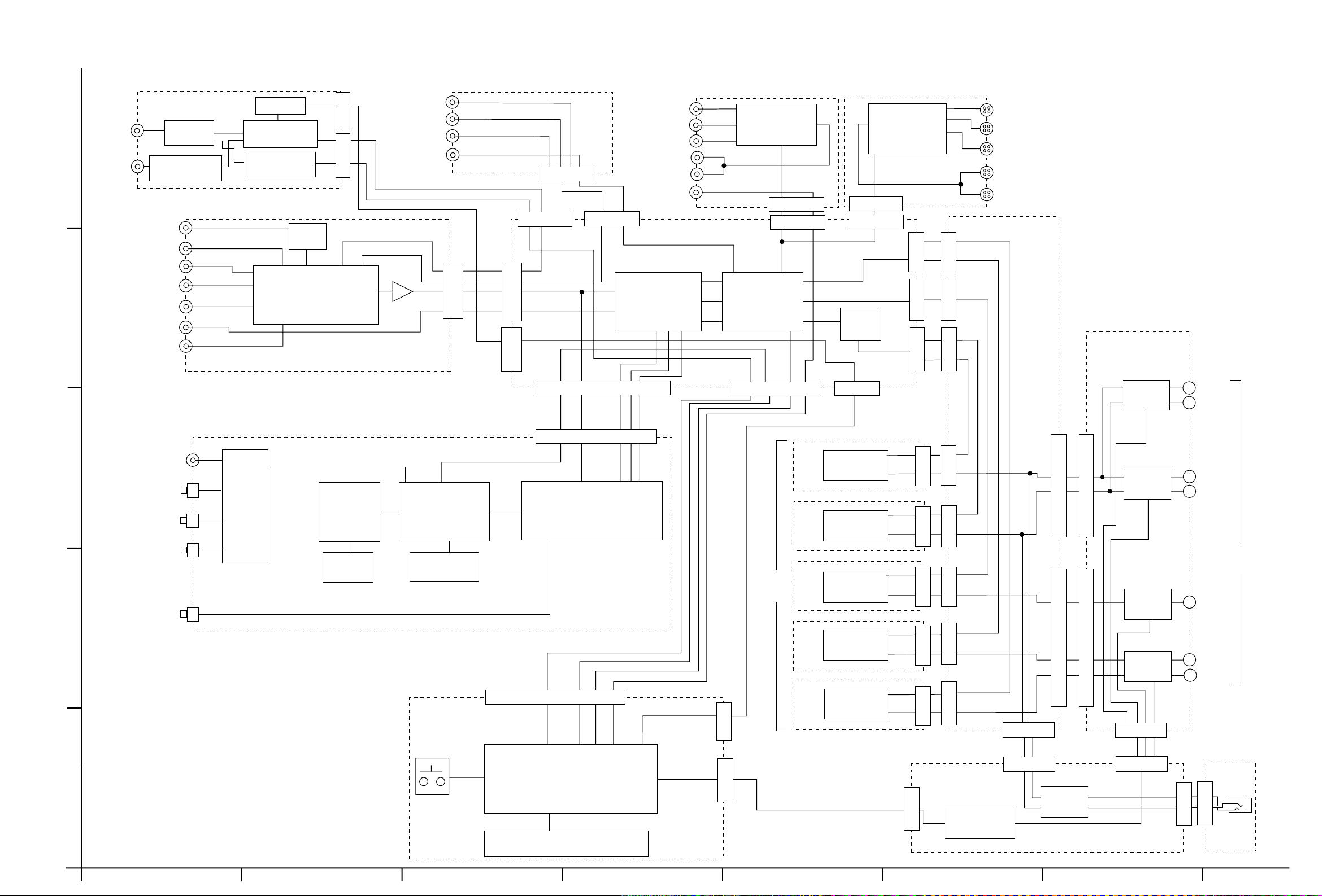
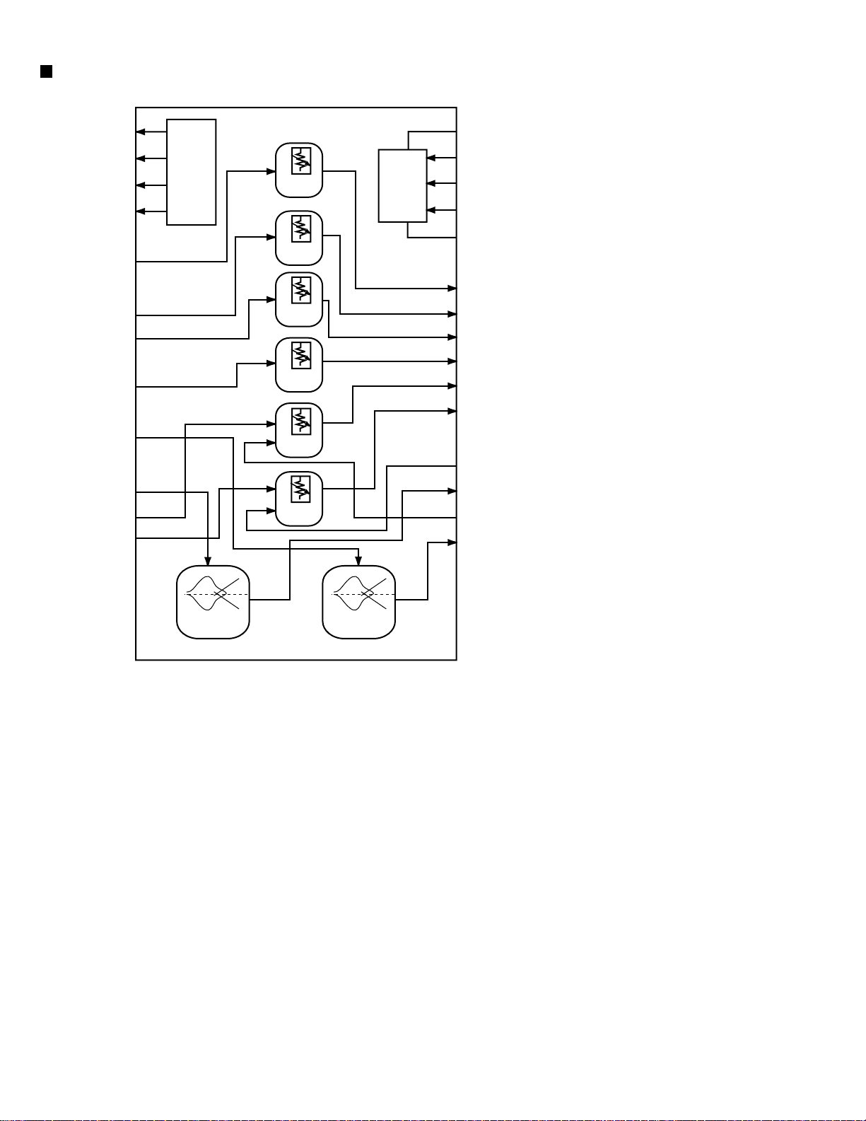
Block diagram
RX-7010RBK/RX-7012RSL
IC191
CN112
FM
TUNER
RF101
5
AM
MW RF&OSC
T111
PHONO
CD
AM/FM DET
IC102
PLL
IC121
EQ
IC401
SENTER/SUBWOOFER
CN111
TUNER
DVD
TAPE P.B.
TAPE REC.
4
VCR P.B.
SOURCE SELECTOR
IC421
VCR REC.
TV SOUND
DVD
DVD
DVD REAR
SUB
WOOFER
TUNER
PLL CLK, PLL DATA, PLLCE,
IC421
CN401
CN411
SIGNAL
VCR OUT
CN421
CN412
CN451
CN431
CN481
DVD
VCR P.B.
TV/DBS
VCR REC
MONITOR
COMPU
LINK
SELECTOR
IC423
SELECTOR
IC501
CN501
CN441
6CH MASTER
VOLUME
IC428
CN402
CN551
CN461
IC421
IC422
CN403
SELECTOR
IC551
IC552
REAR
CN473CN472CN471
CENTER
FRONT
CN373
CN372CN371CN311
DVD
TV/DBS
VCR P.B.
MONITOR
VCR REC
RY301
SPK2
Lch
Rch
CN681
COAXIAL
3
IN
OPTICAL
IN
OPTICAL
IN
SW
IC621
DSP
IC631
OPTICAL
IN
SDRAM
IC641
2
OPTICAL
OUT
1
DSP STATUS, DSP L, DSP COMMAND,
DSP
CONTROLLER
IC671
SELECTOR
IC611
KEY
SYSTEM CONTROLLER
AD/DA CONVERTER
IC681
PLL CLK, PLL DATA, PLLCE,
CN702
IC701
VOLCLK, VOLDATA, VOL LATCH
DSP CLK, DSP STATUS, DSP READY, DSP RESET,
RY HP, RY LR1
RY LR2, RY C
CN703
CN701
AUDIO
AMP.
Lch
Rch
Cch
RLch
RRch
Q315
Q317
Q315
Q317
Q315
Q317
Q315
Q317
Q315
Q317
CN301CN302CN901CN801CN802
CN312
CN321
CN331
CN332
FW341
CN241
FW301
FW302
FW301
FW302
RY302
RY303
RY304
FW303
CN203
SPK1
Lch
Rch
SPEAKER
TERMINAL
Cch
RLch
RRch
HP
RY203
FW251
CN201
Q206~Q209
FW251
FL DISPLAY
D1701
AB CD E F G
2-1
Standard schematic diagrams
Power supply section
5
RX-7010RBK/RX-7012RSL
D206
1SR35-400A
D208
1SR35-400A
PW311
PW302
C208
0.0047/100
D207
C209
470/25
T202
QQT0281-002
1SR35-400A
D209
1SR35-400A
F205
T100mAL
R221
10
10
R203
D210
1SS133
C210
R204
820
C212
470/16
PW203
PW204
PW205
0.0047
RY202
Q203
KTC3203/OY/
D221
1SS133
MTZ6.8JC
D211
Q202
KRC105M
D212
1SR139
PW101
PW102
PW103
PW104
PW105
C213
2200/6.3
T2.5AL
EP1
F201
TA201
TA202
EP201
SHEET
NUMBER
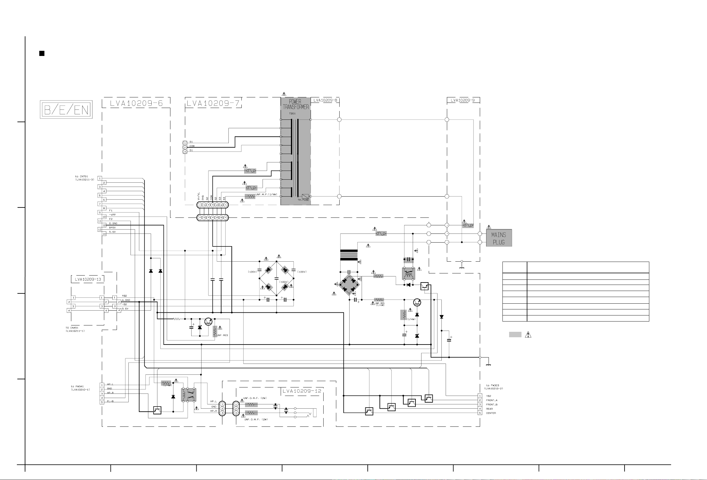
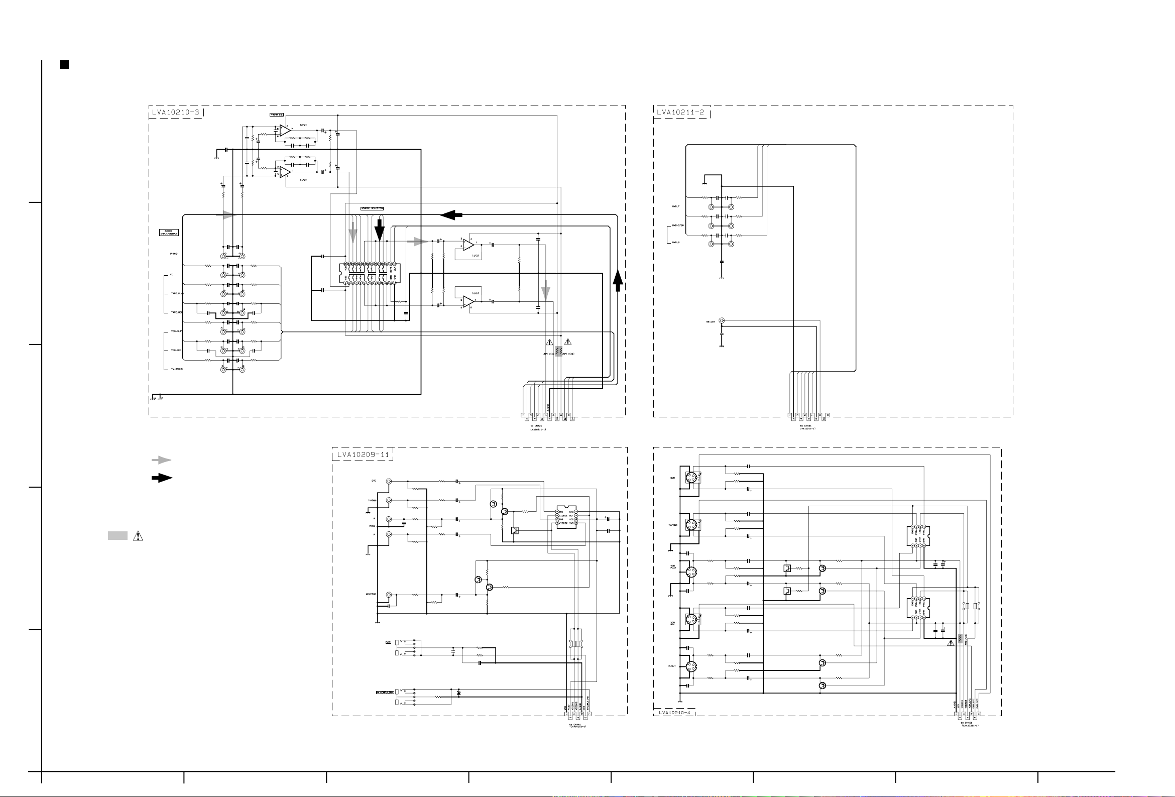
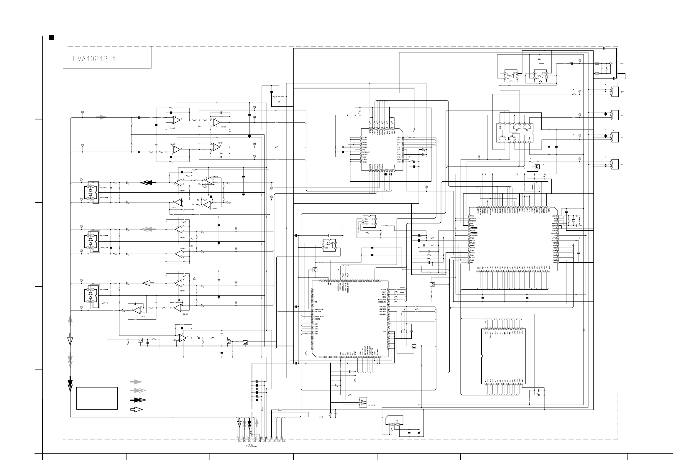
CIRCUIT DESCRIPTION
1 / 8 POWER SUPPLY
2 / 8 SPEAKER TERMINAL
3 / 8 AUDIO AMP
4 / 8 VOLUME / REGULATOR / SOURCE SELECT IC
5 / 8 AUDIO VIDEO SIGNAL INPUT TERMINAL
6 / 8 SURROUND IC / DIGITAL SIGNAL INPUT TERMINAL
7 / 8 USER CONTROL KEY / SYSTEM CONTROL LSI / FL DISPLAY
8 / 8 TUNER
Parts are safety assurance parts.
When replacing those parts make
sure to use the specified.
114
112
CN251
T2AL
T2AL
R201
F202
F203
4.7
4
CN201
RY_HP
RY_LR2
RY_LR1
RY_C
RY_S
PROTECTOR_IN
POWER
Sheet 7/8
RY_SURROUND
FW201
FW201
110
111
113
121
120
122
130
131
014
010
3
D202
1SR35-400A
D201
D219
D220
CN291
CN492 CN292
2
1SR1391SR139
R209
100K
KTC3200/GL
1/50
C218 D217
MTZ6.2JC
0.047
10
C207C206
0.047
Q205
R208
10E2-FD
D203
10E2-FD
C204 C205
2200/35 1000/35
C201
0.1
C203C202
0.10.1
D204
1SR35-400A
CN241
PROTECTOR_IN
Sheet 2/8
1
RY_HP
KRC105M
68
1SS133
D218
Q210
R210
RY203
QSK0109-001
FW251
FW251
R1331
R1332
Q209
RY_S
KRC105M
Q208
RY_LR2
KRC105M
Q207
RY_LR1
CN203
Q206
KRC105M
Sheet 2/8
RY_C
330P
470
C1332
470
C1331
330P
J1331
KRC105M
SHEET 1/8
2-2
HAB C DE FG
RX-7010RBK/RX-7012RSL
Audio & Speaker terminal section
Sheet 1/8
CN351
0.1/160
C1301
C1303
5.6K
C1302
D1301
0.01/500
D1304
0.01/500
C1304
6800/63 6800/63
C1305
D1303
R1304
R1305
R1306
R1307
R1308
R1321
2.2
R1313
C1308
47/50
100K
100K
82K
100K
100K
10
R1314
10K
MTZ20JC
10K
R1320
KTA1046/Y/
D1309
Q1301
C1309
10/25
Q1305
2SD2061/EF/
Q1308
2SC2235/OY/
D1310
MTZ18JC
R1302
5.6K
D1306
MTZ30JC
R1311
100K
Q1303
1SS133
10
R1303
D1308
R1312
100K
R1309
10K
C1311
22/50
Q1302
KTC3200/GL/
R1310
10K
KTC3199/GL/KTA1268/GL/
C1310
47/16
Q1304
R1315
2.2
R1316
1K
KTC3200/GL/
Q1307
1SS133
D1307
Q1306
KTA1023/OY/
R1317
22K
R1319
CN385
FW302
FW301
FW341
FW485
(LVA10211-1)
Sheet 4/8
Sheet 1/8
FW303
FW302
FW301
RY304
QQLZ005-R45
L1351
QQLZ005-R45
L1352
R1353
RY303
QSK0109-001QSK0109-001
C1355
4.7K
R1373
R1361
4.7K
R1372
0.022
R1368
10
R1369
10
C1357
0.022
C1377
0.01
C1359
0.01
R1371
C1352
4.7/50
Q1356
KRC109M
Q1358
C1365
0.047
2.7
C1369
0.022
2.7
R1374
2.7
0.022
C1373
R1370
C1361
0.022
10
10
0.022
C1363
C1366
220P
C1370
220P
C1374
220P
68
QSK109-001
RY301
RY302
QSK109-001
Q1351
KRC109M
R1359
4.7K
Q1352
KRC109M
68
68
R1354
R1364
22K
D1359
R1365
6.8K
1SS133
D1353
D1354
1SS133
4.7/50
R1351
D1351
1SS133
C1378
0.01
C1360
R1355
3.9K
Q1354
KRC109M
R1366
R1367
R1358
22K
0.01
R1357
22K
D1356
MTZ5.1JC
6.8K
Q1355
D1360
C1354
6.8K
4.7/50
QQLZ005-R45
L1353
QQLZ005-R45
L1354
QLZ005-R45
L1355
D1352
R1352
68
1SS133
R1356
4.7K
D1355
1SS133
C1351
4.7/50
R1360
4.7K
D1357
1SS133
D1358
1SS133
Q1353
KRC109M KRC109M
R1362
4.7K
KRC109M KRC109M
Q1357
C1353
R1363
C1356
C1358
C1362
220P
1000P
C1375
220P
C1364
C1368
220P
220P
C1367
C1371
220P
220P
220P
ST302
QNB0001-001
ST301
QNB0104-001
ST303
QNB0101-001
220P
C1372
220P
C1376
Sheet 1/8
SURROUND signal
FRONT signal
R1318
22K
47K
CENTER signal
Parts are safety assurance parts.
When replacing those parts make
sure to use the specified.
5
D1302
CN321
R1301
MTZ22J
C1306
D1305
47/25
4
CN311
CN312
3
CN331
CN332
2
CN373
CN372
Sheet 4/8 Sheet 3/8
CN371
1
AB CD E F G
SHEET 2/8
2-3
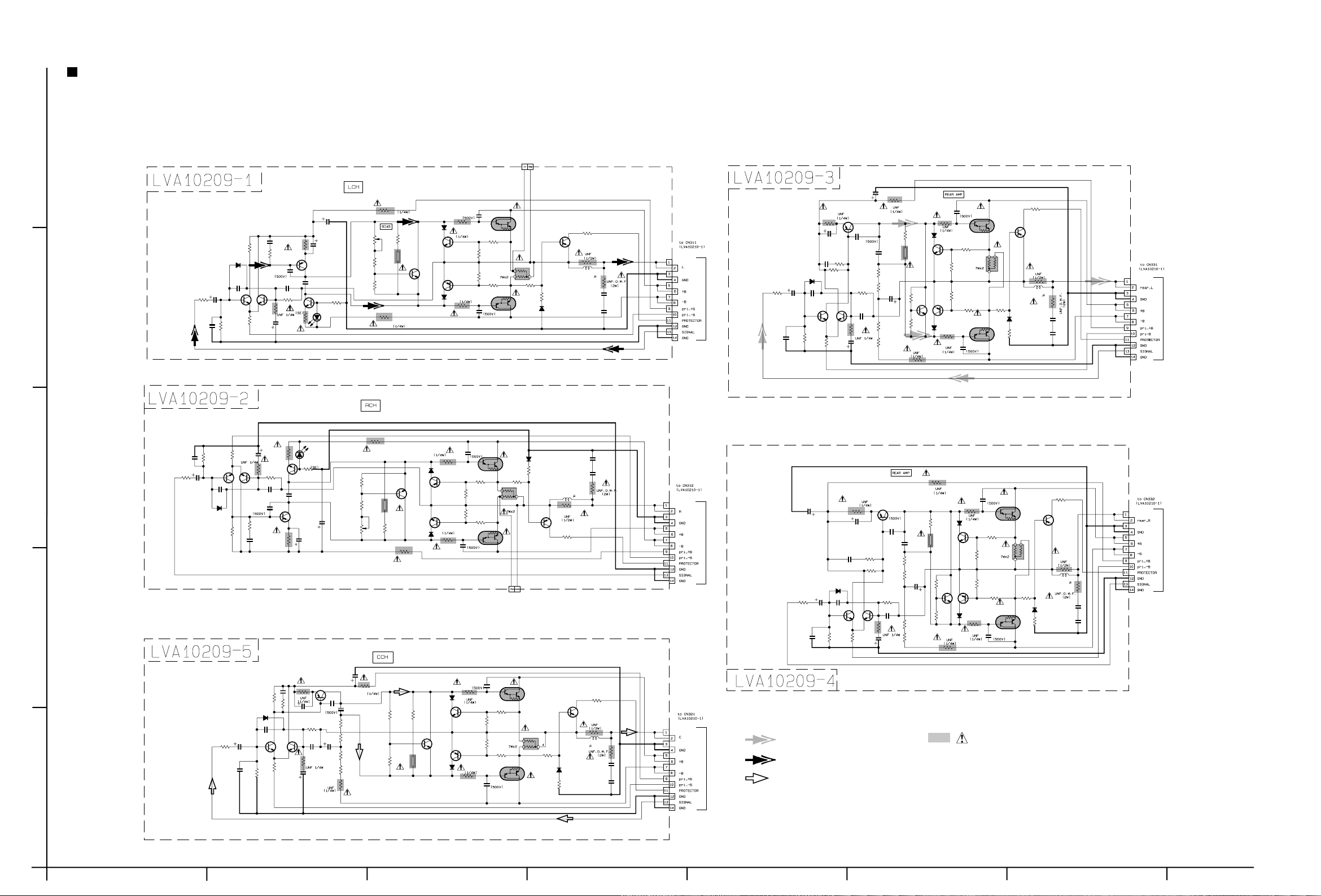
Audio amplirier section
RX-7010RBK/RX-7012RSL
5
R321
10
TH301
QAD0012-202
Q309
QAD0012-202
R322
10
2SD637/QR/
D306
1SS133
D305
1SS133
2SD637/QR/
C307
0.0015
R307
3.3k
D301
1SS133
C305
220P
C301
10/50
R301
Q301
C304
R302
2.2K 10/50
C302
C303
270P
2.2K
R303
56k
R304
56k270P
Q302
2SC2240/L/
C306
220P
D302
1SS133
R308
3.3k
4
3
2SC2240/L/
C310
100/25
R312
390
Q304
2SC2240/L/
R305
12K
C316
R310
22P
100
C308
0.0015
Q303
100
2SC2240/L/
R314
56k
C312
10P
R309
R320R306
C315
R316
22P
C311
C309
100/25
33012K
R311
390
330
R313
C319
100/63
R315
C317
330
47/35
Q305
KTA1268/GL
C313
0.01MY10P
KTC3200/GL
Q307
C318
47/35
47K
SLR-342MC
D304
R318
D303
SLR-342MC
C320
R317
47K
R326
R328
VR302
100/63
56k
R319
330
Q308
KTC3200/GL 10
C314
0.01MY
Q306
KTA1268/GL
R329
VR301
1K
470
R327
470
R325
360
10
R323
R324
10
360
470
R330
Q310
TH302
4701K
C321
47P
10
R331
R339
180
R335
120
R337
0.22
120
R341
180
2SB1560/OPY/-F6
10
Q317
R333 C327
47P
C323
2SB1560/OPY/-F6
47P
Q318
R342
180
R338
120
R336
120
R340
2SD2390/OPY/-F6
Q316
180
C322
47P
KTC3200/GL
Q313
KTA1268/GL
D307
1SS133
10
R334
D308
1SS133
Q314
KTA1268/GL
Q312
KTC3200/GL
10
R332
Q311
C324
2
2SD2390/OPY/-F6
Q315
R343
D310
1SS133
R346
1K
R344
0.22
KTA1268/GL
R345
1K
D309
1SS133
Q320
TP302
TP301
KTA1268/GL
R348
15K
R347
C819
10/100
330
Q805
R815
C817
2.2/50
C807
R807
R805
18k
2SC2240/L/
1SS133
56K
R804
R809
100
3k
Q803
2SC2240/L/
2.2/50
0.0015
D802
C806
220P
KTA1268/GL
33P
R811
390
C809
100/25
R816
330
C818
C808
Q802
R806
2SC2240/L/
C815
0.01MY
R813
56k
C811
10P
2SC2240/L/
18K
R349
47k
Q319
33
R351
L301
R353
0.45
10
C325
15K
0.047MY
0.047MY
C328
0.047MY
C326
0.047MY
RE354
L302
0.45
33
R352
R350
47k
CN302
CN301
Sheet 2/8
C803
R801
270P
0.0015
D801
1SS133
C801
220P
10/50
R803
C805
Q801
56k
10/100
C820
2.2K
Sheet 2/8
C802
10/50
R802
2.2K
C804
270P
R810
100
Q804
R808
3K
10
R829
C813
R855
3.3k
R857
3.3k
47/50
C829
R859
3.3k
R861
3.3k
Q806
KTA1268/GL
C816
C814
0.01MY
R814
56K
10P
C812
R812
390
C810
100/25
R821
470
300
33P
R856
3.3K
R858
47/50
C830
R860
R862
TH801
QAD0012-202
R827
Q809
360
R825
10
R823
R830
470
3.3K
3.3K
3.3K
10
D805
1SS133
KTC3200/GL
Q811
Q813
2SD637/QR/
D807
1SS133
R833
10
R822
TH802
QAD0012-202
R828
300360
R826
C821
R831
180
R835
R837
180
KTA1268/GL
10
1SS133
Q810
2SD637/QR/
10
R824
2SD2390/OPY/-F6
47P
Q815
R839
180
0.22
R841
180
2SB1560/OPY/-F6
Q817
C823
47P
10
R832
D806
KTC3200/GL
Q812
180
Q814
KTA1268/GL
D808
1SS133
R834
10
R836
R838
C822
47P
R840
180
180
C824
R843
R845
1K
2SD2390/OPY/-F6
Q816
R844
0.22
R842
180
2SB1560/OPY/-F6
Q818
47P
D809
1SS133
R847
18K
R846
Q819
1K
R849
12K
KTA1268/GL
33
R851
L801
0.45
R853
C825
0.047MY
C827
0.047MY
Q820
D810
1SS133
R848 C828
10
R850
12K
KTA1268/GL
33
R852
L802
0.45
R854
C826
0.047MY
18K 0.047MY
CN801
Sheet 2/8Sheet 2/8
CN802
10
C919
C917
R913
56k
C911
10P
R911
300
C909
100/25
Q905
KTA1268/GL
C915
33P
R955
3.3k
R957
3.3k
C929
47/50
R961
3.3k
R923
10/100
R921
10
C913
R927
0.01
R959
3.3k
10
R925
300
360
TH901
QAD0012-202
R929
470
1SS133
Q909
D905
2SD637/QR/
D907
1SS133
C907
0.0015
C905
3k
2SC2240/L/
R905
18k
R915
330
100
R909
2.2/50
Q903
2SC2240/L/
R901
2.2K
270P
10/50
C901
R907
D901
1SS133
220P
Q901
R903C903
56k
1
R931
10
Q911
KTC3200/GL
Q913
KTA1268/GL
R933
10
C921
47P
R935
180
R937
180
C923
Q915
2SD2390/OPY/-F6
R939
180
R943
0.22
R941
180
47P
R945
Q917
2SB1560/OPY/-F6
1K
Q919
D909
1SS133
R947
18K
KTA1268/GL
L901
0.45
0.047MY
0.047MY
R949
47k
33
R951
10
R953
C925
C927
CN901
Sheet 2/8
SURROUND signal
FRONT signal
CENTER signal
Parts are safety assurance parts.
When replacing those parts make
sure to use the specified.
SHEET 3/8
2-4
HAB C DE FG
Main section
RX-7010RBK/RX-7012RSL
Sheet 8/8 Sheet 5/8 Sheet 6/8 Sheet 7/8
CN412
5
Sheet 7/8
CN403
R1456
C1438
22
470/6.3
4
R1458
4.7K
C1440
0.0056TF
FL402
QQR0590-001
3
CN431
Sheet 5/8
1K
Q1426
2CS3575-JVC
R1496
2
10K
STEREO_IN
D1406
MTZ10JC
C1407
0.022
R1457
4.7K
C1439
0.0056TF
FL401
QQR0590-001
TU_MUTE
TUNED_IN
C1406
100/25
KTD863/Y/
R1493R1494
1K
Q1425
2CS3575-JVC
PLL_CLK
R1413
10K
CN411
PLL_DATA
PLL_CE
Q1406
1K
R1412
10
R1495
Q1424
KRA104M
D1410
1SS355
D1409
1SS355
SW_CLK
SW_STB
SW_DATA
R1497
510
0.022
C1445
DSP_SL
DSP_C
DSP_R DSP_L
DSP_SR
DSP_LFE
0.022
C1444
R1459
68
S_MUTE
SW_MUTE
2SC3575-JVC
220
R1471
R1474
C1447
4.7/50
R1473
SW_DATA
SW_CLK
CN421
1K
Q1423
KRA104M
R1472
10K
10K
Q1422
Q1421
SW_STB
TC9162AF
IC423
R1465
1K
C1446
220P
68
R1460
R1498
2SC3575-JVC
R1470
DSP_CLK
DSP_RESET
DSP_READY
DSP_STATUS
DSP_COMMAND
510
R490
5.6K
R480
220
15K
R491
15K
5.6K
R489
CN481
DSP_C
DSP_R
DSP_L
DSP_SR
DSP_SL
DSP_LFE
BASSBOOST
S_MUTE
C1434
0.022
D1407
MTZ7.5JC
47/25
0.015MY
PLL_CE
PLL_DATA
DBS
S_MUTE
PLL_CLK
VCR
DVD
R1463
100k
100K
R1455
C1435
0.0082
0.33TF
C1433
C1432
KTD863/Y/
R1415
C1408
100k
BASSBOOST
VIDEO2
VIDEO1
Q1407
2.2K
R1414
IC428
M62446FP
R1499
10
TU_MUTE
SW_MUTE
VOL_CLK
VOL_DATA
VOL_LATCH
R1442
VOL_CLK
100K
VOL_LATCH
VOL_DATA
SW_STB
D1408
MTZ7.5JC
C1409
47/25
SW_CLK
SW_DATA
DCS
AVCOMPULINK
0.0082
0.015MY
0.33TF
TUNED_IN
C1429
C1428
C1427
STEREO_IN
SELF_DET
C1431
4.7/50
C1430
4.7/50
R1441
1K
Q1408
R1417
2.2K
DSP_CLK
DSP_STATUS
DSP_COMMAND
R1416
DSP_RESET
DSP_READY
KTA1023/OY/
10
CN402
KRC104M
Q1416
R1431
10K
D1411
1SS355
C1425
100/10
R1453
1K
Q1420
R1452
100K
R1451
100K
R1447
R1446
100K
C1421
4.7/50
R1436
100K
R1435
100K
R1437
C1420
4.7/50
Q1409
2SK301( P,Q)
R1426 R1427
51K 51K
C1419
0.022MY
4.7K
KRA104M
R1449
1K
R1450
10K
Q1419
2SC3575-JVC
R1448
10K
Q1418
2SC3575-JVC
1K
R1445
1K
R1444
10K
Q1417
2SC3575-JVC
R1438
1K
R1440
10K
Q1414
2SC3575-JVC
R1439
10K
Q1413
2SC3575-JVC
1K
IC421
BA15218F
CN473
CN472
Sheet 2/8
CN471
C1424
4.7/50
C1423
4.7/50
C1461
0.022
C1426
C1436
0.022
10K
R1443
Q1415
KRA104M
C1411
0.022
68
R1419
C1410
0.022
R1418
68
BA15218F
0.022
IC427
BA15218F
R1490
R1492
27K
R1480
1K
100K
C1453
4.7/50
0.022
IC422
4.7/50
C1459
IC427
R1464
BA15218F
C1460
Q1410
2SK301( P,Q)
R1432
10K 10K
C1415
100P
R1422
R1423
10K
2.7K
100P
C1414
10K
2.7K
R1420
R1421
4.7/50
C1412
4.7/50
C1422
100K
B821
Q1412
2SK301( P,Q)
R1434
10K
R1433
10K
Q1411
2SK301( P,Q)
B820
R1430
R1428
10K
10K
R1429
C1413
4.7/50
R1425
4.7K
C1417
0.47/50
0.022MY
C1418
C1416
R1424
0.47/50
C1437
1.5
C1443
1.5ML
DBS
DVD
VCR
VIDEO1
VIDEO2
CN461
1
Sheet 5/8
AUDIO signal
TUNER signal
FRONT signal
CENTER signal
AVCOMPULINK
VIDEO1
VIDEO2
DCS
CN441
Sheet 5/8 Sheet 1/8
0.022
C1464
EP401
R1401
10 12
Q1401
KTA1046/Y/
R1402
1.8K
MTZ13JC
C1401
D1412
47/50
D1401
CN491
Q1402
2SD2395/EF/
R483
1K 1K
100K
R484
1SS355
C1402
100/25
R1403
R1404
R485
2.7K
D1402
MTZ6.2JC
Q1431 Q1432 Q1433
KRC104M KRC104M KRC104M
R1405
12
Q1403
2SD2395/EF/
R1406
6.8k
D1403
MTZ5.6JC
100K
R486
100/25
C1403
Parts are safety assurance parts.
When replacing those parts make
sure to use the specified.
Q1434
R1461
2SD2395/EF/
2.2
Q1404
R1407
2SD2395/EF/
R1462
2.2
R487
1K
R488
100K
100/25
4.7
R1408
4.7
R1409
2.7K
D1404
MTZ5.6JC
C1404
Q1435
2SD2395/EF/
R479
2.2
Q1405
2SD2395/EF/
R478
2.2
R475
20K
27K
R1411
1.8K
D1405
R476
MTZ13JC
100/25
C1405
SURROUND signal
AB CD E F G
FW485
SELF_DET
R477
4.7
R1410
4.7
D1413
1SR35-400A
Sheet 2/8
SHEET 4/8
2-5
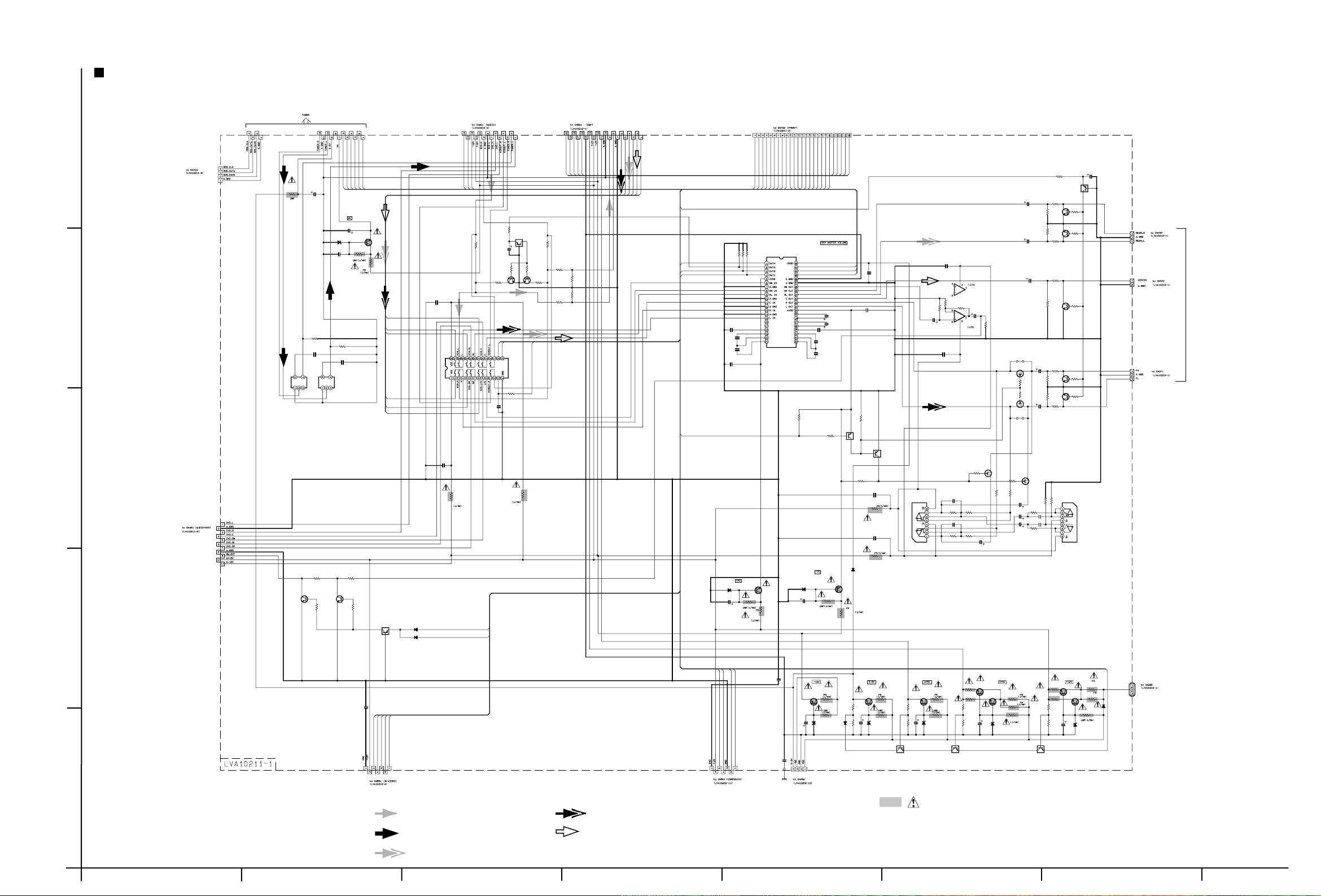
RX-7010RBK/RX-7012RSL
Audio / Video / S Video / DVD signal input section
IC401
C408
NJM4580DD
100P
R406
560
R410 R408
470K 39K
C412 C410
C406
0.0068MY 0.0018MY
5
J401
QNN0389-001
4
J402
QNN0168-001
J403
QNN0168-001
TAPEIN_L
TAPEOUT_L
VCRIN_L
VCROUT_L
TV_L
C400
0.022
J401
QNN0389-001
R401
2.2K
C417 C418
330P 330P
R421 R422
470
C421 C422
330P 330P
R423 R424
470 470
C423 C424
330P
R425 R426
C425 C426
470 470
330P 330P
C427 C428
220P 220P
R429 R430
C429 C430
470 470
330P 330P
R431 R432
C431 C432
470 470
330P 330P
C433
220P 220P
R435 R436
C435 C436
470 470
330P 330P
100/10
R409 R407
470K 39K
C405
47K 47K
100P 100P
C403 C404
R403 R404
C402C401
4.7/504.7/50
R402
2.2K
470
TAPEIN_R
330P
C434
100/10
R405
560
CD_RCD_L
TAPEOUT_R
VCRIN_R
VCROUT_R
TV_R
C407
100P
C411 C409
0.0068MY 0.0018MY
IC401
NJM4580DD
C415
C414
47/16
4.7/50
R412
100K
R411
100K
C416
47/16
C413
4.7/50
J404
QNN0389-001
C441
4.7/50
C419
0.022
C420
0.022
IC402
TC9164AN
CD_L
CD_R
TAPEIN_L
TAPEIN_R
VCRIN_L
VCRIN_R
TV_L
TAPEOUT_L
DVD_L
TUNER_LTUNER_R
SW_DATA
SW_CLK
TV_R
DVD_R
SW_STB
R440
TAPEOUT_R
1K
R441
R443
100K
100K
R442
R444
100K
100K
BA15218N
C442
C440
4.7/50
220P
BA15218N
IC403
C443
4.7/50
IC403
C444
4.7/50
C445
0.022
R445
100k
R446
100k
C446
0.022
R449
R450
270
270
J405
QNN0388-001
J404
R451 R452
470 470
DVD_L
R453
470
DVD_C
R455
470
J406
QNN0284-001
C451
C452
330P
330P
DVD_R
C453
C454
R454
330P
330P
470
DVD_SW
C455
C456
R456
330P
330P
470
DVD_SRDVD_SL
C459
0.1TF
J405
QNN0388-001
C460
1.5MY
J406
QNN0284-001
SW_OUT
DVD_SR
DVD_SL
DVD_SW
DVD_L
DVD_R
DVD_C
A-12V
A+12V
SIG_R
SW_STB
SIG_L
SW_DATA
TUNER_L
TUNER_R
VCROUT_L
VCROUT_R
DVD_L
3
QGB2510K1-14
DVD_R
CN401
SW_CLK
CN451
QGB2510K1-11
A.GND
Sheet 4/8 Sheet 4/8
C551
AUDIO signal
QND0025-001
J552
QND0083-001
QND0083-001
QND0083-001
J551
J551
QND0083-001
J553
J552
C557
47P
R555
75
R556
75
C558
47P
C563
47P
R561
75
75
C564
47P
R501
TUNER signal
2
Parts are safety assurance parts.
When replacing those parts make
J501
QNN0063-001
J503
QNN0017-002
J502
QNN0063-001
J502
QNN0063-001
R502
75
R504
75
R505
75
C504
47P
R508
75
C501
330
4.7/50
R503
C502
330
4.7/50
KTA1267/YG/
C503
470/6.3
R506
47K
R507
C505
330
4.7/50
R511
150
Q501
Q502
KTC3199/GL/
R513
1.5K
R512
270
Q503
KRC101M
IC501
NJM2246D
1000/16
C511
0.022
C512
sure to use the specified.
R514
Q504
KTA1267/YG/
J501
QNN0063-001
J521
QNS0073-001
J591
1
X
R509
75
C507
47P
C506
470/6.3
R510
47K
C521
220P
D591
X
R591
X
150
R516
1.5K
Q505
KTC3199/GL/
R515
270
R522
470
R521
220
C522
QGB2510K1-07
B502
B501
K501
K502
CN501
0.047
R551
75
R552
75
C552
4.7/50
C553
0.047
R553
75
R554
75
C554
4.7/50
C555
0.047
47K
R557
R558
47K
C556
4.7/50
C559
0.047
R559
75
R560
75
C560
470/6.3
C561
0.047
47K
R563
R564
47K
C562
470/6.3
KRC110M
Q573
KRC110M
R573
10K
R574
Q574
KTA1267/YG/
10K
Q553
KTA1267/YG/
Q554
KTA1267/YG/
Q571
KTA1267/YG/
R571
390
R572
390
Q572
R565
390 390
R566R562
C582
1.5ML
C584
1.5ML
IC551
NJM2246D
IC552
NJM2246D
QGB2510K1-07
C581
47/16
K552
K551
B551
B552
C583
47/16
R581
6.8
CN551
2-6
Sheet 4/8
Sheet 4/8
SHEET 5/8
HAB C DE FG
RX-7010RBK/RX-7012RSL
CS
CCLK
MIACK
MILP
MICS
MICK
AUTODATA
DSPSTATUS
DSP_RST
RESET
CCLK
DSP_RST
MICS
MICK
MIACK
AUTODATA
MILP
DSP section
1.0
C628
0.01
IC622IC621
TC7SU04FUTC7SU04FU
5
C608
0.1
R618R617
10K10K
C607
100/16
SMUTE
DSPSTATUS
DSPCLK
LIN+
LIN-
100/6.3
C673
0.01
IC672
TC7SET32FU
C671
0.01
C672
100/6.3
100/6.3 0.01
C688 C687
C611
C612
CSCSCCLK
220
R664
0
R683
0.01
CDTO
220
220
R662
R663
UPD784215AGC103
R688
RIN-
RIN+
0.01
C693
R669
10K
Q672
DTC114YE
0.01
C661
D.MUTE
SELECT1
SELECT2
SELECT3
SELECT4
TEST
10K
R682
0.01
C694
K687
NQR0319-001
R2519
330
R2521
330
R2520
330
TP515
TP514
LFE.MIX
LFE.MIX
K688
NQR0319-001
D.GND
D+5V
A+12V
A-12V
DSPCOMMAND
DSPREADY
RESET
C610
100/6.3
SDTI3
BCLK
LRCLK
SDTI1
SDTI2
R673
4.3K
AUTODATA
LOCK
DIGITAL0
R685
FORMAT
R603
IC683
RN5RZ33BA
10K
CHANNEL
47K
ROUT3
LOUT3
D607
1SS355
D608
1SS355
ERR
RST_DET
X671
NAX0275-001X
SDTO
220
R609
LOUT2
220
R608
ROUT2
DSP_RST
220
R607
IC601
AK4527BVQ
220
220
220
47K
47K
R602
R601
R606
R611
R612
LIN-
LIN+
RIN-
RIN+
C601
C602
0.001
0.001
R632
0R0
R686
150
ERR
R691
220
R692
220
R693
220
R694
220
R695
220
R696
220
Tx
Rx
IC681
PQ3DZ53
10K
R681
R613
8.2K
R615
4.3K
CDTO
CDTI
CCLK
CS
C603
100/6.3
C605
0.1
100/6.3
C604
C606
0.1
TP607
R642
R657
10K
DSPSTATUS
10K
R641
1K
R643
100
0.01
1K
56K
100P
R648
4.7K
10K
C649
120P
LOCK
C641
100/6.3
C642
0.01
0.47
C643
C644
R645
R644
C645
R646
Q607
MIACK
MILP
MICS
MICK
MIDIO
MIDIO
8.2K
R680
DTA144EKA
4.3K
R674
DSPREADY
4.3K
R675
DSPCLK
4.3K
R676
DSPCOMMAND
8.2K
8.2K
100P
C679
R678
R679
Q670
DTC114YE
R670
10K
C690C689
100/6.30.01
TP606
BCLK
LRCLK
WE
CE
OE
I/O5
I/O6
I/O7
A15
A14
A16
C609
0.1
CDTI
220
R661
IC671
C677
100P
8.2K
R677
RESET
0
R671
10K
OUT_LFE
OUT_C
C2555
OUT_SRWEOUT_SL
TP509
TP511
0.1
C2556
0.1
TP510
TP512
C2539
0.1
C2540
0.1
LOUT2
ROUT2
LOUT3
ROUT3
Q673
DTA144EKA
C685
47/16
C683
0.01
C686
47/16
C682
0.01
C684
100/6.3
C681
0.01
K682
NQR0319-001
K681
NQR0319-001
IN_R
IN_L
OUT_R
OUT_L
A+5V
R2515
TP501
IN_L
TP502
IN_R
C2503
R2511 R2513
4.7/50
10k 10k
R2501
100K
R2502 R2522
100K 330
R2512 R2514
C2504
10k 10k
4.7/50
4
TP503
OUT_L
IC652
IMX9-W
TP504
OUT_R
TP505
OUT_SL
IC662
OUT_SR
OUT_C
OUT_LFE
IMX9-W
TP506
TP507
IC682
IMX9-W
TP508
3
R2529
10K
R2530
10K
R2567
10K
R2568
10K
R2587
10K
R2588
10K
2
C2527
R2525
10/50
1K
C2525
R2527
0.001
100K
C2526
R2528
0.001
100K
R2526
C2528
1K
10/50
C2577
R2575
10/50
1K
C2575
R2577
0.001
100K
C2576
R2578
0.001
100K
R2576
C2578
1K
10/50
C2597
R2595
10/50
1K
C2595
R2597
0.001
100K
R2598
100K
R2596
C2598
1K
4.7/25
DTA144EKA
R2560 C2500
1M
C2592
0.022
R2594
33k
IC691
BA15218F
R2590
33k
Q2501
R2500
22/16
10k
C2515
120p
C2513
IC609
0.0012
BA15218F
IC609
BA15218F
C2514
0.0012
C2516
120p
R2516
10k
IC651
BA15218F
C2552
56P
C2594
0.1
R2584
22K
R2592
33k
R2557
10K
SMUTE
IC691
BA15218F
1K
C2551
56P
R2553
15K
IC651
BA15218F
15K
R2554 R2556
C2563
22P
IC661
BA15218F
IC661
BA15218F
C2564
22P
C2583
22P
IC690
BA15218F
C2584
56P
R2586
3.3K
IC690
BA15218F
22K
R2558
56P
C2587
R2517
10k
R2518
10k
R2555
8.2K
R2531
7.5K
R2551
10k
R2552
10k
R2532
R2563
10k
R2565
2K2K100K
R2566
R2564
10k
R2583
12K
R2585 R2581
3K 100K
C2517
390p
C2518
390p
7.5K
8.2K
C2561
1.0/50
R2561
R2562
100K
C2562
1.0/50
C2581
1.0/50
R2582
100K
C2582
10/16
C2588
4.7/25
R2589
100K
C2507
33p
R2509
R2507
22k
22k
IC610
BA15218F
C2512
0.1
IC610
BA15218F
R2508
R2510
22k
22k
33p
C2508
IC650
BA15218F
C2533
4.7/50
R2535
C2531
56P
10k
R2537
10k
56p
R2536
IC650
BA15218F
R2550
2.7k
Q671
2SD2114K/VW
100k
R2538
100k
10k
C2534
4.7/50
C2569
0.1
TP517
C2570
0.1
TP518
C2589
TP519
0.1
C2590
0.1
TP520
C2585
0.1
C2586
R672
0.1
1M
R2533
C2532
R2534
10K
AUDIO signal
Note
X :None used
1
SURROUND signal
FRONT signal
CENTER signal
CN681
QGB2510K1-20
R628
18K
SELECT3
SELECT4
SELECT2
R639
SDTI2
SDTI3
A0
A1A2A3A4A5A6A7
OE
SDTI1
IC631
TC9446F-014
I/O6
I/O7CEA10
I/O0A0A1A2A3A4A5A6A7
4.7K
I/O4
I/O5
I/O2
I/O1
SDTO
I/O0
I/O1
I/O2
I/O3
I/O4
A11A9A8
A13
IC641
W24L010AJ-12
A12
R627
4.7K
IC611
BU4066BCF
C639
C638
0.01
100/6.3
SELECT1
R633
220
Q601
DTC114YE
D.MUTE
C631
C632
100/6.3
0.01
MIDIO
MILP
DSP_RST
MICS
MICK
MIACK
A8
A9
A10
A11
A12
A13
A14
A15
A16
C634C633
0.10.1
I/O3
C653
0.1
C654
0R0
100/6.3
R640
R621
220
C646
0.01
AUTODATA
ERR
FORMAT
CHANNEL
DIGITAL0
RST_DETLOCK
1/50
C621
R629
100
R623
100
R625
100
2.2M
R647
NAX0385-001X
C636
TP601
TP602
TP603
TP604
TP605
C647
22P
X631
C648
18P
0.1
0.1
C635
LC631
NQR0321-001
K601
NQR0269-004
C622
100P
K602
NQR0269-004
C627
J601
R622
75
QNN0347-001
C626
0.1
C629
0.1
UN664
GP1FA550RZ
C624
0.1
UN661UN662
GP1FA550RZGP1FA550RZ
C625
0.1
C637
0.1
UN663
GP1FA550TZ
Sheet 4/8
AB CD E F G
SHEET 6/8
2-7
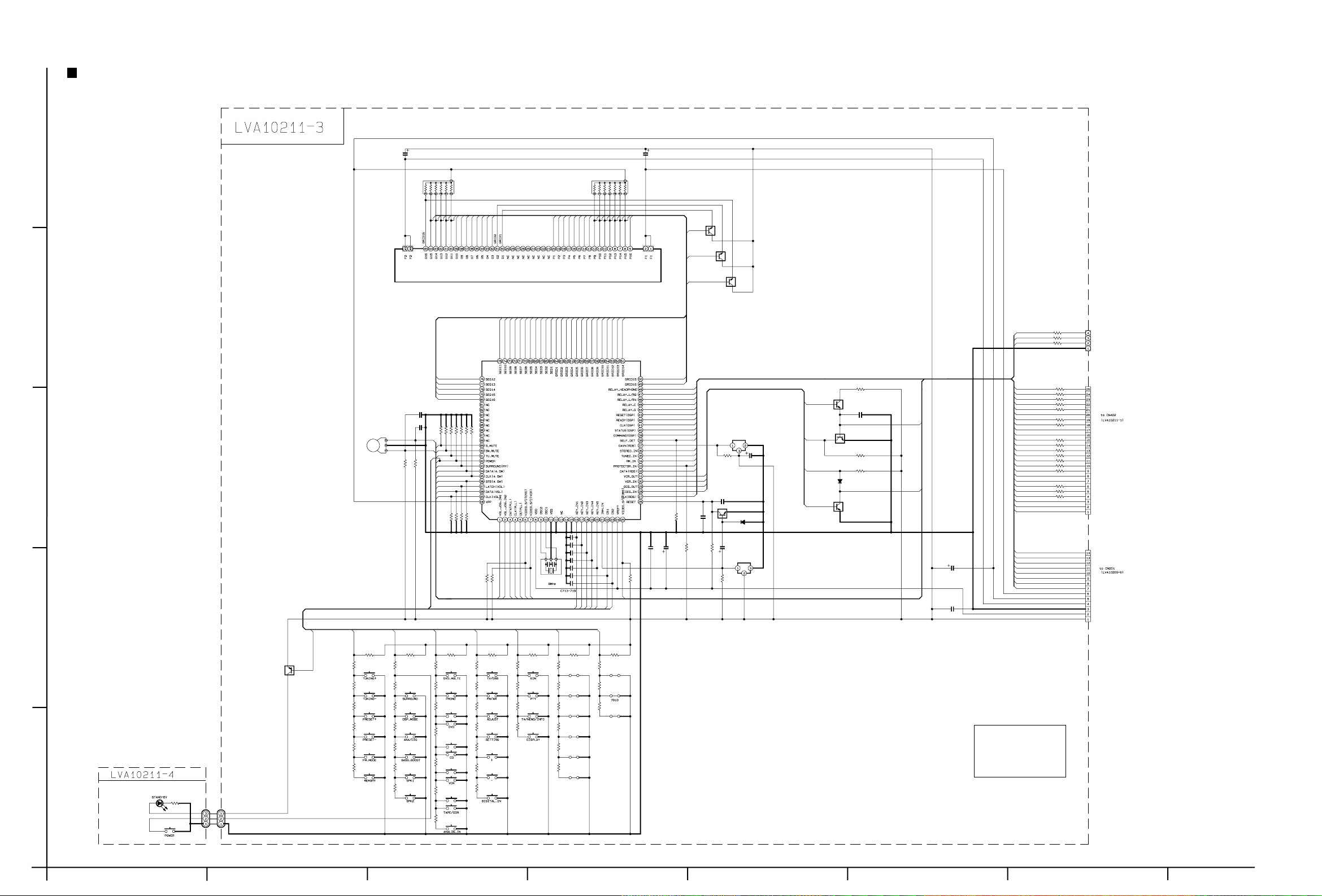
RX-7010RBK/RX-7012RSL
System control and FL displaying section
C707C709
5
QRB089J-104QRB079J-104
RA702RA701
GRID15
GRID10
GRID14
GRID12
GRID11
GRID13
GRID9
GRID8
GRID7
GRID6
GRID5
GRID4
GRID3
DI701
QLF0082-001
SEG6
SEG5
SEG4
SEG3
SEG2
SEG1
SEG13
SEG12
SEG11
SEG10
SEG9
SEG8
SEG7
4.7/504.7/50
GRID1
Q707
SEG16
SEG15
SEG14
DTC114Y
GRID2
GRID16
Q708
DTC114Y
DTC114Y
Q709
4
CN703
RDS_CLK
RDS_DATA
RDS_DAVN
SEG11
SEG10
SEG9
SEG8
SEG7
SEG6
SEG5
SEG4
SEG3
SEG2
SEG1
GRID1
GRID2
GRID3
GRID4
GRID5
GRID6
GRID7
GRID8
GRID9
GRID10
GRID11
GRID12
GRID13
GRID14
220
R782
R781
220
R780
220
QJK021-043004
SEG12 GRID15
SEG13
SEG14
SEG15
C721
0.1
C720
0.1
JOG2
JOG1
JS701
3
QSW0898-001
R759
R760
10k
10k
SEG16
10k
10k
10k
10k
10k
10k
IC701
PLL_DATA
PLL_CLK
PLL_CE
S/C_DVD
S/C_VCR
MN101C35D
QAX0246-001
X701
KEY_IN5
KEY_IN4
KEY_IN3
KEY_IN2
KEY_IN1
C713
C714
C715
C716
C717
C718
C719
0.01
CS2
CS1
R716
R718
R717
R720
R757
R758
R775
10k
10k
10k 10k
10k
R712
R713
R714
R715
JOG1
JOG2
10k
10k
R707
R708
2
POWER
Q711
DTA144E
1
D719
SLR-342VC
R719
220
S727
QSW0683-001
CN714
CN704
QUM133-08DGZ4
QUM133-08DGZ4
KEY_IN1
R722
1k
R723
1k
R724
1.2k
R725
1.5k
R726
2.2k
R727
2.7k
QSW0683-001
KEY_IN2
R721
10k
R729
1k
S721
R730
1k
S722
R731
1.2k
S723
R732
1.5k
S724
R733
2.2k
S725
R734
2.7k
S726
R735
3.9k
KEY_IN3
R728 R736 R743 R750 R761 R768
10k 10k 10k 10k 10k 10k
R737
1k
R738
1k
S728
R739
1.2k
S729
R740
S730
1.5k
S731
R741
2.2k
S732
R742
2.7k
S733
R773
3.9k
KEY_IN4
R744
1k
S734
R745
1k
S735
R746
1.2k
S736
S754
X
R747
1.5k
S737
R748
2.2k
S755
X
R749
S738
2.7k
S756
X
R774
3.9k
S739
S757
X
S752
X
KEY_IN5
R751
1k
S740
R752
1k
S741
R753
1.2k
S742
R754
1.5k
S743
S744
S745
S753
X
CS1
R762
1k
S746
R763
1k
S747
R764
1.2k
S748
R765
1.5k
S749
R766
2.2k
R767
2.7k
CS2
R769
1k
B701
X
R770
1k
B702
EUR
R771
1k
B703
X
B704
X
B705
X
B706
X
B707
B708
S/C_DBS
GRID16
RY_HP
RY_LR2
RY_LR1
RY_C
RY_S
DSP_RESET
DSP_READY
DSP_CLK
DSP_STATUS
DSP_COMMAND
SELF_DET
RDS_DAVN
STEREO_IN
TUNED_IN
RM_IN
PROTECTOR_IN
RDS_DATA
VCR_OUT
VCR_IN
DCS_OUT
DCS_IN
RDS_CLK
C730
R711
0.1
100k
R710
C701
C702
1.5ML 100/6.3
10k
R709
10k
IC703
GP1U281X
R703 C705
10k 100/6.3
C704
0.022
Q701
DTC114YE
D701
1SS355
R702
C703
22k
2.2/50
IC702
IC-PST9139
R701
4.7k
DCS_OUT
DCS_IN
VCR_IN
VCR_OUT
Q702
DTC114TE
Q703
DTC144WE
D702
1SS355
Q704
DTC114YE
R704
470
C706
330p
DCS
R705
10k
R706
10k
VCR
C708
4.7/50
C722
1.5
DSP_RESET
DSP_READY
DSP_CLK
DSP_STATUS
DSP_COMMAND
SELF_DET
STEREO_IN
TUNED_IN
VCR
DCS
SW_DATA
SW_CLK
SW_STB
VOL_LATCH
VOL_DATA
VOL_CLK
TU_MUTE
SW_MUTE
S_MUTE
PLL_DATA
PLL_CLK
PLL_CE
S/C_DBS
S/C_DVD
S/C_VCR
R799
R798
R797
R796
R795
R794
R793
R792
R791
R790
R789
R788
R787
R786
R785
R784
R783
220
220
220
220
220
220
220
220
220
220
220
220
220
220
220
220
220
QGF1205C1-25
RY_HP
RY_LR2
RY_LR1
RY_C
RY_S
PROTECTOR_IN
POWER
RY_SURR
F1
-VPP
F2
B+5V
5V
QGF1205C1-14
CN702
Sheet 4/8
CN701
Sheet 1/8
X
B709
X
Note
X :None used
SHEET 7/8
2-8
HAB C DE FG
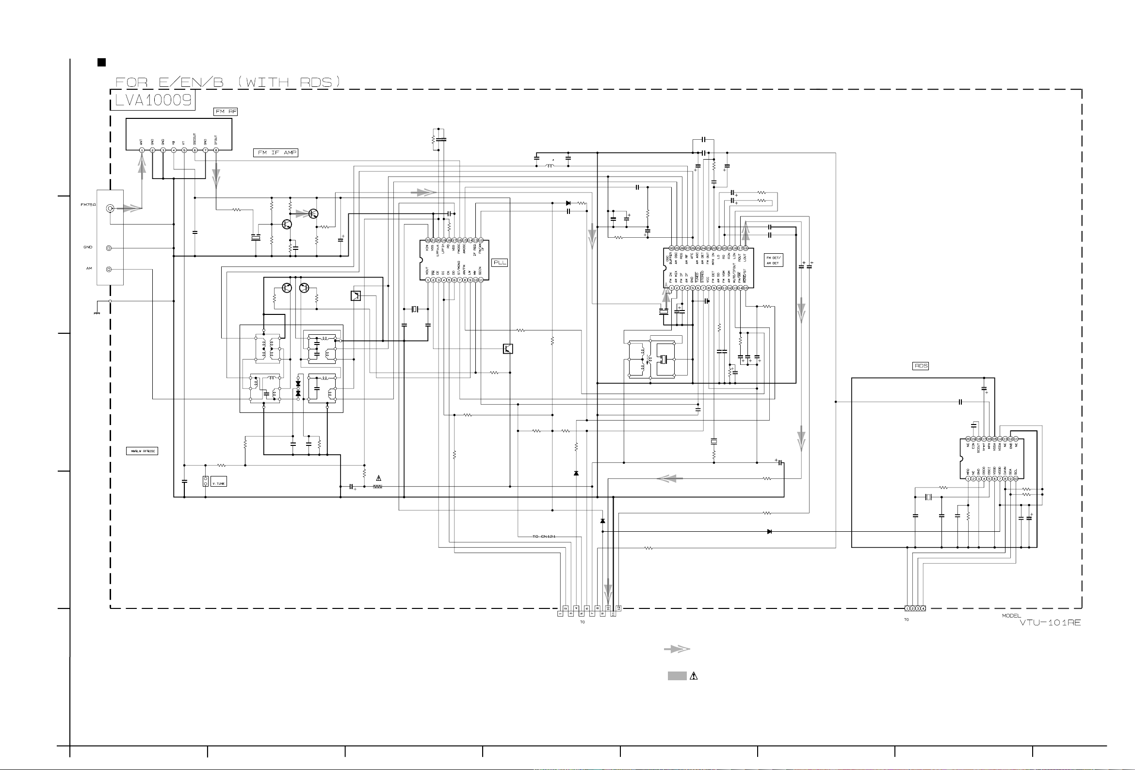
RX-7010RBK/RX-7012RSL
Tuner section
C129
IC121
LC72136N
X121
QAX0402-001
C121
C122
12P
12P
R127
0.001
C128
0.47/50
8.2K
R124
C117
6P
C123
0.047
2.2K
R126
5.6K
Q121
DTA124E
R114
1.2K
R184
R134
1K
10K
R183
10K
L111
15
D129
1SS133
R122
4.7K
C126
100P
R182
10K
R133
3.9K
D123
1SS133
C118
15P
R132
39K
C157
0.047
R147
3.3K
T142
QQR0973-001
1SS133
D121
C158
22/16
C156
0.001
R146
4.7K
C168
1/50
CF102
QAX0285-001Z
R141
1K
IC102
LA1838
C150
22/16
C143
0.022
C133
22/16
C141
0.047
C134
0.0022
C137
68P
C144
R150
330
0.047
R140
56K
C135
0.022
470.022
R142C163
0.047
C164
CF103
QAX0519-001Z
5.6k
R143
C147
1/50
R144
C136
R157
C161
10/16
2.7K
C162
10/16
R158
2.7K
C139
0.039
C140
0.039
C186
10/16
C185
10/16
R145
10K
3.3K
C148
1/50
0.22/50
1/50
C149
C146
1/50
C196
2.2/50
C195
330P
560P
C193
C184
R161
1K
R162
1K
D131
1SS133
100/16
C191
82P
X191
QAX0263-001Z
C192
47P
R191
1K
C194
IC191
SAA6588
R193
10K
R194
10K
R192
470K
0.1
C199
C197
10/16
0.047
RF101
5
C101
0.01
4
AT101
QNB0014-001
BK001
QAU0119-001
R103
100
CF101
QAX0285-001Z
R104
2.7K
390
R105
Q111
KTC3199/GL
R111
4.7k
R107
560
1K
R106
Q102
2SC535/BC
0.022
C105
Q112
KTC3199/GL
Q103
2SC461/BC
R112
4.7k
R109
R108
220
C107
22/16
3.3K
Q113
DTA114Y
3
T111T111T111T111T111
T111T111T111T111
T111T111T111T111T111
T111T111T111T111T111T111
T111T111T111T111T111T111T111T111T111
QQR0871-001
C112
C111
0.047
12P
100K
R115
R128
4.7K
C130
100/10
R130
68( 1/4W) F.RES.
C103
0.022
R129
TP101TP101
R119
10K
2.2K
2
DAVN
SDA
SCL
CN111
QGB2501K2-12
DATA
MUTE
CKCE9V
STEREO
TUNED
CN411
DETOUT
5.6V
LOUT
ROUT
GND
sheet 4/8
QGB2501K1-04
CN112
D.GND
CN412
sheet 4/8
FM / Tuner signal
1
AB CD E F G
Parts are safety assurance parts.
When replacing those parts make
sure to use the specified one.
SHEET
8/8
2-9
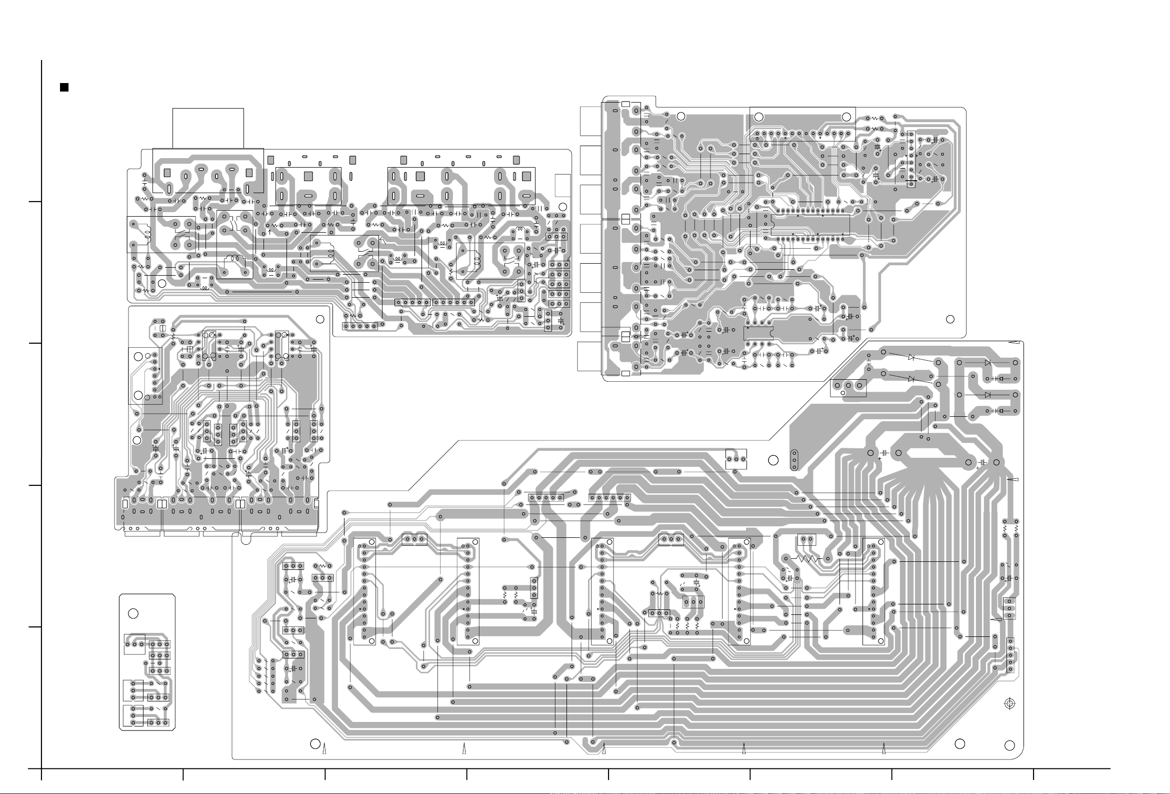
Printed circuit boards
Main board
RX-7010RBK/RX-7012RSL
R440
C416
C415
CN351
C440
R449
R450
R445
R446
C1301
C1304
C443
C444
D1302
D1304
C446
C445
IC403
R444
R443
C442
R442
R441
C441
C1305
D1303
D1301
C1302
C1303
R1302
R1303
C435
R435
R436
5
ST302
C556
R556
C558
Q574
IC552
R557
R558
RY302
Q571
Q572
C584
C557
B432
C1358
C583
R555
R552
Q573
C555
C1378
R571
C552
C1359
R551
R573
L1352
R1370
C551
C1364
C1360
C1362
C1361
IC551
R566
Q554
R563
R564
R562
C563
C564
J551
C582
R1371
C581
R565
Q553
C561C562
R561
C1377
R1368
C1355
RY301
D1351
4
R1351
D1352
R1352
K552
B552
CN551
3
C554
C553
R553
R554
J553
R560
R559
C560
C1357
R581
B551
R1369
C1356
B1005
L1351
K551
R572
R574
C559
J552
R1354
FW303
C1363
R1374
D1354
ST303ST301
C1374C1375
RY304
L1355
C1373
C1376
FW301
R1365
L1354
R1373
R1364
D1359
R1353
FW302
C1370
D1353
C1371C1372
C1369
R1355
R1357
R1372
RY303
C1368
D1355
C1351
C1366
Q1351
R1358
L1353
R1359
R1356
Q1358
R1363
D1356
R1362
C1365
R1361
R1360
D1357
D1358
C1352
C1367
R1366
C1354
R1367
Q1356
Q1355
Q1353
Q1354
Q1352
Q1357
D1360
C1353
FW301
J403
J402
J401
FW302
C424
C429C430
C425C426
C421
C400
C418
C432
C431
R429
R401
R430
C422 C423
C417
R432
C436
R431
R422
C433
R423
R424
R425
C427
C428
R426
R402
C434
C402
C401
R421
R403 R404
C403 C404
R406
C406
R405
C405
C407 C408
CN385
IC401
R409
R410
C412
C411
C420
C419
CN401
R408
C410
C409
R407
IC402
C414
R412
R411
C413
EP301
CN311
D1305
CN372
C1306
R1301
D1306
C1308
CN321
Q1301
FW341
HAB C DE FG
2
Q1302
C1309
R1309
R1311
R1307
R1306
R1305
R1308
R1304
Q1304
R1310
CN210
Q233
Q234
B200
Q235
R232
1
CN208CN209
Q232
R231
Q231
R1317
Q1307
R1319
R1318
Q1303
C1310
R1312
D1307
CN332
CN373
CN331
R1321
R1320
D1310
C1312
Q1308
CN312
D1308
R1316
Q1306
CN371
B379
D1309
R1315
R1313
C1311
Q1305
R1314
2-10
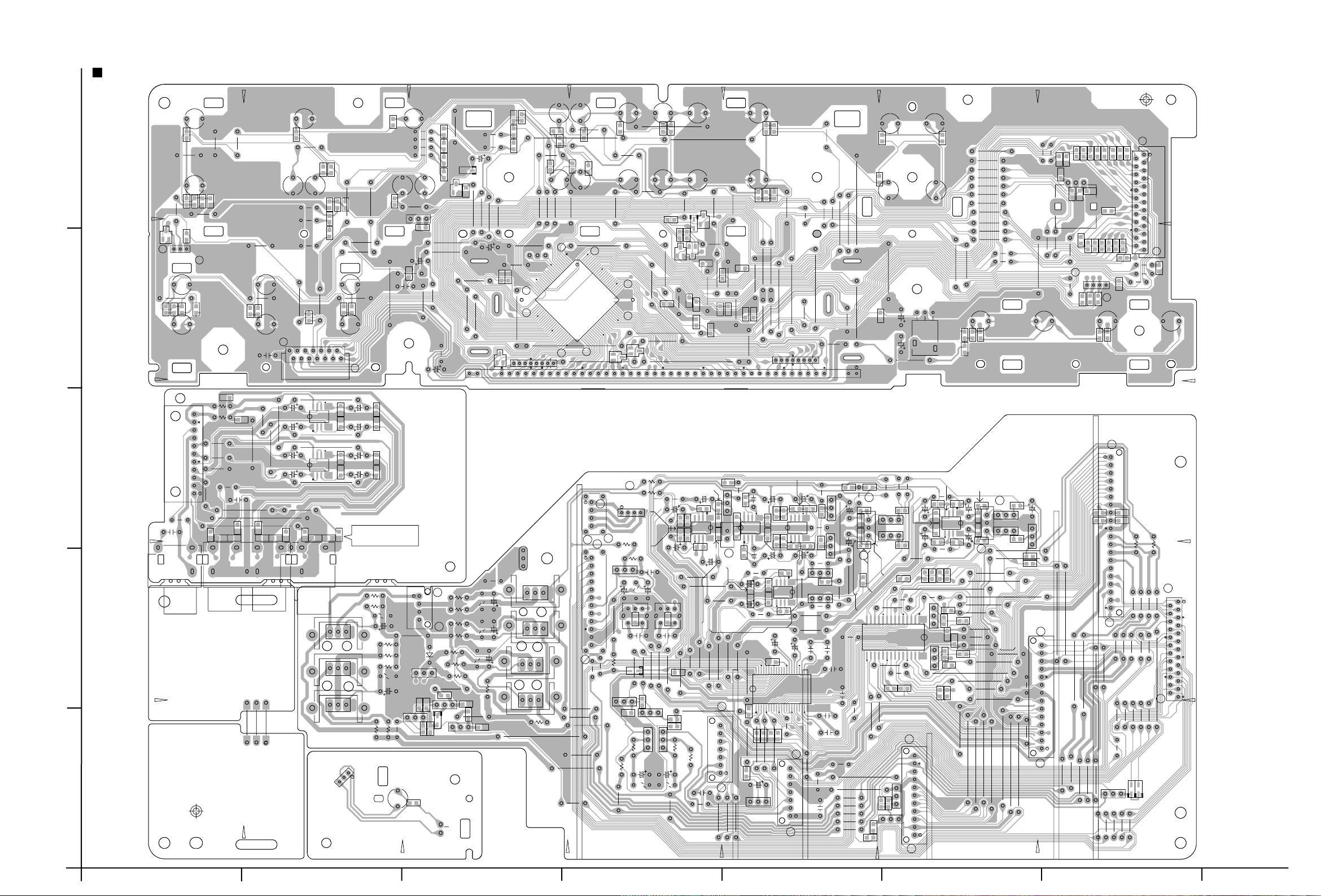
System control & Audio board
RX-7010RBK/RX-7012RSL
B754
CN412
S755
B1718
R739
S754
Q708
Q1415
S736
B753
CN411
R741
B1717
R1412
C1438
R1458
R1456
R1443
R1416
S737
B729
CN403
FL402
R1413
C1440
D1411
R1417
D1408
B728
Q1406
S757
S756
R1419
R1491R1492
D1406
Q1408
Q707
R1418
C1452
R706
B780
R1479R1480
R1431
D1407
R773
B1706
IC427
C1406
Q1407
R762R763
B733
C718
C730
B1703
B732
B781
RA701
R761
S735
R738
B731
R737
R736
S734
B758
B757
B756
X701
IC701
EP401
R479
Q1401
Q1403
Q1435
Q1405
R740
C715
B755
B1702
B1711
HS401
HS403
HS435
HS405
R725
S732
C719
C462
C461
B769
R455
R727
B767
C455
R735
B704
B706
R772
B786
IC702
R710
S726
B1744
R461R462
R471R472
C453
C454
C456
R453
R456
R1403
D1402
C1402
D1404
C1404
R1462
R1461
R734
B737
R732
R733
S752
S730
B707
B708
B709
S724
B788
R757
CN701
C464
C463
IC451
C474
C473
IC471
HS434
Q1434
B787
R768
R769
R770R771
B768
B770
R726
S725
R463
R464
R474
C472
C471
R473
J404
R1404
HS402
Q1402
Q1404
HS404
CN714
S729
R731
B744
B742
B743
5
S728
R721
CN451
R729
S722
R728
C713
B740
R482
C714
B739
B738
R724
S723
C722
C481
R481
C482
B741
R730
Q711
R720
CN704
B771
4
R722
R723
S721
3
C459
C460
J406
J405
2
R454
S751
B703
B705
C702
R451
Q1432
C708
CN491
R1408
R1407
R1409
C451
C452
R452
R701
FW485
R487
S733
B702
B762
B761
C704
B1704
R486
B783
D1405
D701
B782
D1401
D1403
R475
R702
B760
C1403
B701
B759
C701
Q709
B833
C1401
C1405
R478
R476
B763
R764R765R766
C703
S731
R767
Q701
B1752
B1751
B764
B735
B1728
C709
R1402
R1401
R1405
R1406
R1411
D1413
R1410
R477
R485
R488
R484
Q1431
D1412
Q1433
R483
1
R719
S727
D719
S739
B1710
B1713
R742
S738
Q704
B726
D702
B752
B1716
B727
FL401
R1441
R1442
R1415
R1457
C712
C1459
Q702
C1443
R715
C1422
R1414
C706
R1490
R718
R1446
R1464
R704
B777
B778
R709
R1445
R1427
R705
Q703
B794
R717
B779
DI701
R1489
C1453
C1407
C1439
C1426
Q1416
C1408C1409
Q1417
C1414
R707
C711
R1420
R1421
R1484
B751
B724
R714
C1449
C1448
CN461
B776
C1411
IC421
C1410
R1425
R1483
B750
R1429
R1454
R1474
R708
R775
B749
R1424
Q1423
S741
R758
C1447
S740
B775
R1455
R1426
C1436
R743
C1418C1419
C1417
B793
B774
R1432
R1463
R744 R745
C1416
B792
B747
RA702
IC422
R1499
R746
C716
B1709
R1423
R1476
R1481
R1475
C1412
R1482
B748
C1431
C1415
C1432
B1708
R1422
IC425
C1413
CN441
B720
R1433
C1430
R1428
B1727
B1712
IC428
C1428
C1437
Q1412
C1429
C1433
C1434
B723
B710
B719
R1430
B716
Q1411
Q1409
C1427
C1435
Q1410
B1748
B718
C1420
IC423
B1747
B1705
C1421
R1434
B1749
C1460C1461
R1496
R1437
R1493
R1495
R747
R1435R1436
R1438
R1494
R748
Q1413
Q1414
Q1425
S742
R703
R496
S744
CN471
B1746
C705
C707
R1439
R1440
C1446
R492
B773
Q1426
IC703
R1477 R1478
R1487
C1450 C1451
R497
S745
CN431
S743
R1488
Q1421
Q1422
R498
R493
IC426
R495
R749
R1498
R1486
R1485
B789
R1470
R499
R494
R750
C717
R1497
C1423
C1424
B1743
R1472
R1473
R751
R1449
R1447
R1451R1452
B1742
B1733
B1734
B1735
B1736
B1737
B746
B1738
B1741
B1740
B1739
R752
S746
CN473
Q1418
Q1419
R1453
R1465
C1444
R1471
R1448
R1450
C1445
B1725
B1726
B1745
S747
CN421
C1425
B1723
Q1420
B1732
B1724
C721
B1731
R713
B1722
R712
JS701
R760
R790
B1730
R490
R489
R759
R792
R782
R789
R793
R781
R788
R794
R780
R787
C720
R753
R791
R795
R786
Q1424
R796
R754
R785
S748
R797
R799
B1719
B1720
R784
R711
R783
CN702
R798
CN481
R480
R491
B1721
D1409
D1410
R1460
R716
S749
R1459
CN402
AB CD E F G
2-11
 Loading...