


SERVICE MANUAL
AUDIO/VIDEO CONTROL RECEIVER
RX-5042S
|
|
|
|
|
|
|
|
|
|
|
|
|
|
|
|
|
|
|
|
|
|
|
|
|
|
|
|
|
|
|
|
|
|
|
Area suffix |
|
|
|
|
|
|
|
|
|
|
|
|
|
|
|
|
|
|
|
|
|
|
|
|
|
|
|
|
|
|
|
|
J ----------------------------- |
U.S.A. |
||
|
|
|
|
|
|
|
|
|
|
|
|
|
|
|
|
|
|
|
|
|
|
|
|
|
|
|
|
|
|
|
|
C -------------------------- |
Canada |
||
|
|
|
|
|
|
|
|
|
|
|
|
|
|
|
|
|
|
|
|
|
|
|
|
|
|
|
|
|
|
|
|
|
|
|
|
|
|
|
|
|
|
|
|
|
|
|
|
|
|
|
|
|
|
|
|
|
|
|
|
|
|
|
|
|
|
|
|
|
|
|
|
|
|
|
|
|
|
|
|
|
|
|
|
|
|
|
|
|
|
|
|
|
|
|
|
|
|
|
|
|
|
|
|
|
|
|
|
|
|
|
|
|
|
|
|
|
|
|
|
|
|
|
|
|
|
|
|
|
|
|
|
|
|
|
|
|
|
|
|
|
|
|
|
|
|
|
|
|
|
|
|
|
|
|
|
|
|
|
|
|
|
|
|
|
|
|
|
|
|
|
|
|
|
|
|
|
|
|
|
|
|
|
|
|
|
|
|
|
|
|
|
|
|
|
|
|
|
|
|
|
|
|
|
|
|
|
|
|
|
|
|
|
|
|
|
|
|
|
|
|
|
|
|
|
|
|
|
|
|
|
|
|
|
|
|
|
|
|
|
|
|
|
|
|
|
|
|
|
|
|
|
|
|
|
|
|
|
|
|
|
|
|
|
|
|
|
|
|
|
|
|
|
|
|
|
|
|
|
|
|
|
|
|
|
|
|
|
|
|
|
|
|
|
|
|
|
|
|
|
|
|
|
|
|
|
|
|
|
|
|
|
|
|
|
|
|
|
|
|
|
|
|
|
|
|
|
|
|
|
|
|
|
|
|
|
|
|
|
|
|
|
|
|
|
|
|
|
|
|
|
|
|
|
|
|
|
|
|
|
|
|
|
|
|
|
|
|
|
|
|
|
|
|
|
|
|
|
|
|
|
|
|
|
|
|
|
|
|
|
|
|
|
|
|
|
|
|
|
|
|
|
|
|
|
|
|
|
|
|
|
|
|
|
|
|
|
|
|
|
|
|
|
|
|
|
|
|
|
|
|
|
|
|
|
|
|
|
|
|
|
|
|
|
|
|
|
|
|
|
|
|
|
|
|
|
|
|
|
|
|
|
|
|
|
|
|
|
|
|
|
|
|
|
|
|
|
|
|
|
|
|
|
|
|
|
|
|
|
|
|
|
|
|
|
|
|
|
|
|
|
|
|
|
|
|
|
|
|
|
|
|
|
|
|
|
|
|
|
|
|
|
|
|
|
|
|
|
|
|
|
|
|
|
|
|
|
|
|
|
|
|
|
|
|
|
|
|
|
|
|
|
|
|
|
|
|
|
|
|
|
|
|
|
|
|
|
|
|
|
|
|
|
|
|
|
|
|
|
|
|
|
|
|
|
|
|
|
|
|
|
|
|
|
|
|
|
|
|
|
|
|
|
|
|
|
|
|
|
|
|
|
|
|
|
|
|
|
|
|
|
|
|
|
|
|
|
|
|
|
|
|
|
|
|
|
|
|
|
|
|
|
|
|
|
|
|
|
|
|
|
|
|
|
|
|
|
|
|
|
|
|
|
|
|
|
|
|
|
|
|
|
|
|
|
|
|
|
|
|
|
|
|
|
TABLE OF CONTENTS
1 PRECAUTION. . . . . . . . . . . . . . . . . . . . . . . . . . . . . . . . . . . . . . . . . . . . . . . . . . . . . . . . . . . . . . . . . . . . . . . . . 1-3 2 SPECIFIC SERVICE INSTRUCTIONS . . . . . . . . . . . . . . . . . . . . . . . . . . . . . . . . . . . . . . . . . . . . . . . . . . . . . . 1-5 3 DISASSEMBLY . . . . . . . . . . . . . . . . . . . . . . . . . . . . . . . . . . . . . . . . . . . . . . . . . . . . . . . . . . . . . . . . . . . . . . . 1-6 4 ADJUSTMENT . . . . . . . . . . . . . . . . . . . . . . . . . . . . . . . . . . . . . . . . . . . . . . . . . . . . . . . . . . . . . . . . . . . . . . . 1-13 5 TROUBLESHOOTING . . . . . . . . . . . . . . . . . . . . . . . . . . . . . . . . . . . . . . . . . . . . . . . . . . . . . . . . . . . . . . . . . 1-14
COPYRIGHT © 2004 VICTOR COMPANY OF JAPAN, LIMITED
No.MB171
2004/3

SPECIFICATION
Amplifier
Output Power
At Stereo operation |
Front channels |
100 W per channel, min. RMS, driven into 8 Ω |
, 40 Hz to 20 kHz with |
|
|
no more than 0.8% total harmonic distortion. |
|
|
|
|
|
At Surround operation |
Front channels |
100 W per channel, min. RMS, driven into 8 Ω |
, at 1 kHz with no more |
|
|
than 0.8% total harmonic distortion. |
|
|
|
|
|
|
Center channel |
100 W, min. RMS, driven into 8 Ω , at 1 kHz with no more than 0.8% |
|
|
|
total harmonic distortion. |
|
|
|
|
|
|
Surround channels |
100 W per channel, min. RMS, driven into 8 Ω |
, at 1 kHz with no more |
|
|
than 0.8% total harmonic distortion. |
|
Audio |
|
|
|
|
|
|
|
Audio Input Sensitivity/ |
CD, TAPE/CDR, VCR, TV SOUND, DVD:220 mV/47 kΩ |
|
|
Impedance (1 kHz) |
|
|
|
|
|
|
|
Audio Input (DIGITAL IN)* |
Coaxial |
DIGITAL 1 (DVD):0.5 V(p-p)/75 Ω |
|
|
|
|
|
|
Optical |
DIGITAL 2 (CD):-21 dBm to -15 dBm (660 nm ±30 nm) |
|
|
|
|
|
* Corresponding to Linear PCM, Dolby Digital, and DTS Digital Surround (with sampling frequency-32 kHz, 44.1 kHz, 48 kHz)
Recording Output Level |
TAPE/CDR, VCR:220 mV |
|
|
|
|
Signal-to-Noise Ratio('66 IHF/'78 IHF) |
CD, TAPE/CDR, VCR, TV SOUND, DVD:87 dB/74 dB |
|
|
|
|
Frequency Response (8 Ω ) |
CD, TAPE/CDR, VCR, TV SOUND, DVD:20 Hz to 50 kHz (+1 dB, -3 dB) |
|
|
|
|
Bass Boost |
+3 dB ±1 dB at 100 Hz (Only for RX-6040B/RX-6042S) |
|
|
|
|
Equalization (5 bands) |
63 Hz, 250 Hz, 1 kHz, 4 kHz, 16 kHz (±8 dB in 2 dB steps) |
|
|
|
|
Video |
|
|
|
|
|
Video Input Sensitivity/Impedance |
Composite video:DVD, VCR |
1 V(p-p)/75 Ω |
|
|
|
Video Output Level |
Composite video:VCR, MONITOR OUT |
1 V(p-p)/75 Ω |
|
|
|
Synchronization |
Negative |
|
|
|
|
Signal-to-Noise Ratio |
45 dB |
|
|
|
|
|
FM tuner (IHF) |
|
|
|
|
Tuning Range |
87.5 MHz to 108.0 MHz |
|
|
|
|
Usable Sensitivity |
Monaural:12.8 dBf (1.2 µV/75 Ω ) |
|
|
|
|
50 dB Quieting Sensitivity |
Monaural:16.0 dBf (1.7 µV/75 Ω ) |
|
|
|
|
|
Stereo:37.5 dBf (20.5 µV/75 Ω ) |
|
|
|
|
Stereo Separation at OUT (REC) |
35 dB at 1 kHz |
|
|
|
|
|
AM tuner |
|
|
|
|
Tuning Range |
530 kHz to 1 710 kHz |
|
|
|
|
|
General |
|
|
|
|
Power Requirements |
AC 120V , 60 Hz |
|
|
|
|
Power Consumption |
200 W/260 VA (at operation):2 W (in standby mode) |
|
|
|
|
Dimensions (W × H × D) |
435 mm × 146.5 mm × 369.5 mm (17 3/16 in. × 5 13/16 in. × 14 5/8 in.) |
|
|
|
|
Mass |
7.5 kg (16.6 lbs) |
|
|
|
|
Designs and specifications are subject to change without notice.
1-2 (No.MB171)
SECTION 1 PRECAUTION
1.1Safety Precautions
(1)This design of this product contains special hardware and many circuits and components specially for safety purposes. For continued protection, no changes should be made to the original design unless authorized in writing by the manufacturer. Replacement parts must be identical to those used in the original circuits. Services should be performed by qualified personnel only.
(2)Alterations of the design or circuitry of the product should not be made. Any design alterations of the product should not be made. Any design alterations or additions will void the manufacturers warranty and will further relieve the manufacture of responsibility for personal injury or property damage resulting therefrom.
(3)Many electrical and mechanical parts in the products have special safety-related characteristics. These characteristics are often not evident from visual inspection nor can the protection afforded by them necessarily be obtained by using replacement components rated for higher voltage, wattage, etc. Replacement parts which have these special safety characteristics are identified in the Parts List of Service Manual. Electrical components having such features are identified by shading on the schematics and by (  ) on the Parts List in the Service Manual. The use of a substitute replacement which does not have the same safety characteristics as the recommended replacement parts shown in the Parts List of Service Manual may create shock, fire, or other hazards.
(4)The leads in the products are routed and dressed with ties, clamps, tubings, barriers and the like to be separated from live parts, high temperature parts, moving parts and/or sharp edges for the prevention of electric shock and fire hazard. When service is required, the original lead routing and dress should be observed, and it should be confirmed that they have been returned to normal, after reassembling.
(5)Leakage shock hazard testing
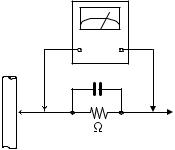
After reassembling the product, always perform an isolation check on the exposed metal parts of the product (antenna terminals, knobs, metal cabinet, screw heads, headphone jack, control shafts, etc.) to be sure the product is safe to operate without danger of electrical shock.Do not use a line isolation transformer during this check.
•Plug the AC line cord directly into the AC outlet. Using a "Leakage Current Tester", measure the leakage current from each exposed metal parts of the cabinet, particularly any exposed metal part having a return path to the chassis, to a known good earth ground. Any leakage current must not exceed 0.5mA AC (r.m.s.).
•Alternate check method
Plug the AC line cord directly into the AC outlet. Use an
AC voltmeter having, 1,000Ω per volt or more sensitivity in the following manner. Connect a 1,500Ω 10W resistor paralleled by a 0.15µF AC-type capacitor between an exposed metal part and a known good earth ground.
Measure the AC voltage across the resistor with the AC
voltmeter.
Move the resistor connection to each exposed metal part, particularly any exposed metal part having a return path to the chassis, and measure the AC voltage across the resistor. Now, reverse the plug in the AC outlet and repeat each measurement. Voltage measured any must not exceed 0.75 V AC (r.m.s.). This corresponds to 0.5 mA AC (r.m.s.).
AC VOLTMETER (Having 1000 ohms/volts,
or more sensitivity)
0.15 F AC TYPE
|
Place this |
|
probe on |
1500 10W |
each exposed |
metal part. |
Good earth ground
1.2Warning
(1)This equipment has been designed and manufactured to meet international safety standards.
(2)It is the legal responsibility of the repairer to ensure that these safety standards are maintained.
(3)Repairs must be made in accordance with the relevant safety standards.
(4)It is essential that safety critical components are replaced by approved parts.
(5)If mains voltage selector is provided, check setting for local voltage.
1.3Caution
Burrs formed during molding may be left over on some parts of the chassis.
Therefore, pay attention to such burrs in the case of preforming repair of this system.
1.4Critical parts for safety
In regard with component parts appearing on the silk-screen printed side (parts side) of the PWB diagrams, the parts that are printed over with black such as the resistor (  ), diode (
  ) and ICP (
  ) or identified by the "
  " mark nearby are critical for safety. When replacing them, be sure to use the parts of the same type and rating as specified by the manufacturer.
(This regulation dose not Except the J and C version)
(No.MB171)1-3

1.5Importance administering point on the safety
Primary part
(Power / Fuse board)
Secondary parts
(Power transformer board 1)
F201
6.3A-125V
|
|
|
|
F202 |
|
F206 |
|
|
F207 |
|
F203 |
5A-125V |
|
|
5A-125V |
2A-125V |
2A-125V |
|
|
|
|
|
|
|
|
|
|
|
|
|
|
|
|
|
|
Caution: For continued protection against risk of fire, replace only with same type 6.3A/125V for F201, 2A/125V for F202 and F203, 5 A/125 V for F206 and F207.
This symbol specifies type of fast operating fuse.
Precaution: Pour eviter risques de feux, remplacez le fusible de surete de F201 comme le meme type que 6,3 A/125 V, 2 A/125 V pour F202 et F203, et 5 A/125 V pour F206 et F207.
^
Ce sont des fusibles suretes qui functionnes rapide.
1-4 (No.MB171)
SECTION 2
SPECIFIC SERVICE INSTRUCTIONS
This service manual does not describe SPECIFIC SERVICE INSTRUCTIONS.
(No.MB171)1-5

SECTION 3
DISASSEMBLY
3.1 Removing the top cover (See Fig.1)
(1)From the right and left sides of the main body, remove the four screws A attaching the top cover.
(2)From the back side of the main body, remove the three screws B attaching the top cover.
(3)Remove the top cover in the direction of the arrow 2 while extending the lower sections of the top cover in the direction of the arrow 1.
3.2 Removing the front panel assembly (See Figs.2 and 3)
•Prior to performing the following procedures, remove the top cover.
(1)Disconnect the card wire from the connector CN402 on the front board. (See Fig.2.)
(2)Disconnect the card wire from the connector CN201 on the power supply board. (See Fig.2.)
(3)Remove the tie band and remove the wire protection board fixing the card wire. (See Fig.2.)
(4)Remove the three screws C attaching the front panel assembly. (See Fig.2.)
(5)From the bottom side of the main body, remove the four screws D attaching the front panel assembly. (See Fig.3.)
(6)Remove the front panel assembly in the direction of the arrow. (See Fig.3.)
Wire protection board |
Front panel assembly |
|
Tie band |
|
|
C |
C |
CN201 C |
|
|
Card wire |
B
2
Top cover
1
|
1 |
|
A |
|
A |
|
Fig.1 |
|
Front panel assembly |
D |
D |
Fig.3
Card wire
Power supply board
CN402
Front board
Fig.2
1-6 (No.MB171)

3.3 Removing the rear panel (See Fig.4)
•Prior to performing the following procedures, remove the top cover.
(1) |
From the back side of the main body, remove the strain |
E |
|
relief from the rear panel in the direction of the arrow. |
|
(2) |
Remove the twenty-one screws E attaching the rear panel. |
|
Rear panel
3.4 Removing the tuner (See Fig.5)
•Prior to performing the following procedures, remove the top cover.
(1)Disconnect the card wire from the connector CN411 on the front board.
(2)Take out the tuner.
Card wire
3.5 Removing the DSP board, audio input board, DVD board and video board (See Fig.6)
E
Fig.4
CN411
Tuner
Fig.5
•Prior to performing the following procedures, remove the top cover and rear panel.
(1)From the top side of the main body, disconnect the DSP board from the connector CN481 and CN482 on the front board.
(2)Disconnect the audio input board from the connector CN421 on the front board.
(3)Disconnect the DVD board from the connector CN431 on the front board.
(4)Disconnect the video board from the connector CN441 on the front board.
|
|
|
|
|
|
|
|
|
|
|
Audio input board |
||||||||||||||||||||
|
|
DSP board |
|
|
|
|
|
|
|
Video board |
|||||||||||||||||||||
|
|
|
|
|
|
|
|
|
|
|
|
|
|
|
|
|
|
|
|
|
|
|
|
|
|
|
|
|
|||
CN481 |
|
|
|
|
|
|
|
|
|
|
|
|
|
|
|
|
|
|
|
DVD board |
|||||||||||
|
|
|
|
|
|
|
|
|
|
|
|
|
|
|
|
|
|
|
|
|
|
|
|
|
|
|
|
|
|
|
|
|
|
|
|
|
|
|
|
|
|
|
|
|
|
|
|
|
|
|
|
|
|
|
|
|
|
|
|
|
|
|
|
|
|
|
|
|
|
|
|
|
|
|
|
|
|
|
|
|
|
|
|
|
|
|
|
|
|
|
|
|
|
|
|
|
|
|
|
|
|
|
|
|
|
|
|
|
|
|
|
|
|
|
|
|
|
|
|
|
|
|
|
|
|
|
|
|
|
|
|
|
|
|
|
|
|
|
|
|
|
|
|
|
|
|
|
|
|
|
|
|
|
|
|
|
|
|
|
|
|
|
|
|
|
|
|
|
|
|
|
|
|
|
|
|
|
|
|
|
|
|
|
|
|
|
|
|
|
|
|
|
|
|
|
|
|
|
|
|
|
|
|
|
|
|
|
|
|
|
|
|
|
|
|
|
|
|
|
|
|
|
|
|
|
|
|
|
|
|
|
|
|
|
|
|
|
|
|
|
|
|
|
|
|
|
|
|
|
|
|
|
|
|
|
|
|
|
|
|
|
|
|
|
|
|
|
|
|
|
|
|
|
|
|
|
|
|
|
|
|
|
|
|
|
|
|
|
CN421 |
CN441 |
|
CN482 |
CN431 |
Front board |
|
|
|
||
Fig.6
(No.MB171)1-7

3.6 Removing the front board (See Fig.7)
•Prior to performing the following procedures, remove the top cover, rear panel, DSP board, audio input board, DVD board, video board and tuner.
(1)From the top side of the main body, disconnect the card wire from the connector CN402 on the front board.
(2)Disconnect the relay board from the connectors (CN291, CN491) on the power supply board and front board.
(3)Disconnect the wires from the connectors CN471, CN472 and CN473 on the front board.
(4)Remove the two screws F attaching the front board.
(5)Loosen the screw G attaching the front board.
(6)Take out the front board from the main body.
3.7 Removing the speaker terminal board (See Fig.8)
•Prior to performing the following procedure, remove the top cover and rear panel.
From the top side of the main body, remove the solders from the soldered sections a on the speaker terminal board.
Power supply board
Card wire CN471 Relay board |
|
|
|||
CN473 |
CN472 |
CN291 |
|||
|
|
||||
|
|
|
|||
|
|
|
|
|
|
|
|
|
|
|
|
|
|
|
|
|
|
|
|
|
|
|
|
F
G
CN402
Front board |
CN491 |
F |
|
|
Fig.7 |
Parallel wires
Soldered sections a
Speaker terminal board
Fig.8
1-8 (No.MB171)

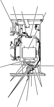
3.8 Removing the main board (See Fig.9)
•Prior to performing the following procedures, remove the top cover.
(1)From the top side of the main body, remove the tie bands fixing the wires.
(2)Remove the tie band and remove the wire protection board fixing the card wire.
(3)Remove the solders from the soldered sections b on the speaker terminal board attaching the parallel wires.
(4)Disconnect the relay board from the connectors (CN291, CN491) on the power supply board and front board.
(5)Disconnect the parallel wire from the connector CN241 on the power supply board.
(6)Disconnect the wire from the connector CN251 on the power transformer board 1.
(7)Disconnect the wires from the connectors CN471, CN472 and CN473 on the front board.
(8)Remove the screw G, two screws H and four screws J attaching the main board.
(9)Take out the main board from the main body.
3.9 Removing the heat sink (See Figs.10 and 11)
•Prior to performing the following procedures, remove the top cover and main board.
(1)Remove the three screws K attaching the heat sink. (See Fig.10.)
(2)From the reverse side of the main board, remove the two screws L attaching the heat sink. (See Fig.11.)
3.10 Removing the power ICs (See Figs.11)
•Prior to performing the following procedures, remove the top cover, main board and heat sink.
(1)From the reverse side of the main board, remove the solders from the soldered sections c on the main board.
(2)Take out the power ICs.
Wire protection board |
|
||
Main board |
|
||
|
Relay board |
Power supply board |
|
|
|
||
J |
Tie bands J |
CN241 |
|
|
|
||
Tie band |
|
Tie band |
|
|
|
||
|
|
CN251 |
|
J |
|
CN291 |
|
|
|
Power |
|
K |
|
transformer |
|
|
board 1 |
||
|
|
G |
|
Card wire |
|
|
|
CN473 |
|
Parallel wires |
|
|
CN491 |
||
Front board |
|
||
Speaker terminal board |
|||
|
|||
CN471 |
|
||
|
CN472 |
|
|
|
Soldered sections b |
||
|
Fig.9 |
|
|
Heat sink |
K |
Main board |
Power IC |
Fig.10 |
|
Soldered section c |
Heat sink |
L 


 L
L
Main board
Fig.11
(No.MB171)1-9
3.11 Removing the power transformer (See Fig.12)
•Prior to performing the following procedures, remove the top cover.
(1)From the top side of the main body, remove the tie bands fixing the wires.
(2)Remove the solders from the soldered section d on the power transformer board 1.
(3)Remove the solders from the soldered sections e on the power transformer board 2.
(4)Disconnect the wire from the connector CN251 on the power transformer board 1.
(5)Remove the four screws M attaching the power transformer.
(6)Take out the power transformer from the main body.
3.12 Removing the power/fuse board (See Fig.12)
•Prior to performing the following procedures, remove the top cover.
(1)From the back and top sides of the main body, remove the screw N and screw P attaching the power/fuse board.
(2)Remove the solders from the soldered sections f attaching the power cord.
(3)From the reverse side of the power/fuse board, remove the solders from the soldered sections g attaching the wires.
Power transformer board 1 |
|
|
Tie band |
Soldered section d |
|
CN251 |
Power transformer |
|
|
|
|
M


 M
M
M
 M
M
Power |
P |
|
transformer |
||
|
||
board 2 |
|
|
Soldered sections e |
|
|
|
N Soldered sections g |
|
Soldered sections g |
Power / Fuse board |
|
|
||
|
Soldered sections f |
|
Power cord |
||
|
Fig.12 |
|
1-10 (No.MB171)
3.13 Removing the power supply board (See Fig.13)
•Prior to performing the following procedures, remove the top cover.
(1)From the top side of the main body, disconnect the parallel wires from the connectors CN203 and CN241 on the power supply board.
(2)Disconnect the card wire from the connector CN201 on the power supply board.
(3)Disconnect the relay board from the connector CN291 on the power supply board.
(4)Remove the tie band fixing the parallel wire.
(5)Disconnect the parallel wire from the connector CN101 on the headphone jack board.
(6)Remove the solders from the soldered section d on the power transformer board 1.
(7)Remove the three screws Q and screw R attaching the power supply board.
(8)From the reverse side of the power supply board, remove the solders from the soldered sections h attaching the wires.
3.14 Removing the headphone jack board (See Figs.13 and 14)
•Prior to performing the following procedures, remove the top cover and front panel assembly.
(1)From the top side of the main body, remove the tie band fixing the parallel wire. (See Fig.13)
(2)Disconnect the parallel wire from the connector CN101 on the headphone jack board. (See Fig.13)
(3)From the front side of the main body, remove the special nut and screw S attaching the bracket (phones) to the front bracket. (See Fig.14)
|
Q |
|
Card wire Power supply board |
CN241 |
CN201 Parallel wire |
|
Tie band |
|
CN101 |
Parallel wires |
Headphone |
CN203 |
jack board |
|
|
|
Q |
CN291 |
Soldered |
|
section h |
Q |
R |
Relay board |
Soldered section d |
|
Power transformer board 1
Fig.13
Headphone jack board
Special nut
Bracket(phones)
S
Front bracket
Fig.14
(No.MB171)1-11
3.15 Removing the system control board and power switch board (See Figs.15 and 16)
•Prior to performing the following procedures, remove the top cover and front panel assembly.
(1)Pull out the volume and jog knobs from the front side of the front panel assembly, remove the nut attaching the system control board. (See Fig.15)
(2)From the back side of the front panel assembly, remove the nine screws T attaching the system control board. (See Fig.16)
(3)Disconnect the parallel wire from the connector CN714 on the power switch board. (See Fig.16)
(4)Take out the system control board from the front panel assembly.
(5)Remove the two screws U attaching the power switch board. (See Fig.16)
(6)Take out the power switch board from the front panel assembly.
Front panel assembly
Nut
Volume knob
|
Jog knob |
|
Fig.15 |
|
Front panel assembly |
|
Parallel wire |
T |
CN714 |
U
T
T
System control board |
Power switch board |
Fig.16
1-12 (No.MB171)
SECTION 4
ADJUSTMENT
This service manual does not describe ADJUSTMENT.
(No.MB171)1-13
SECTION 5
TROUBLESHOOTING
This service manual does not describe TROUBLESHOOTING.
1-14 (No.MB171)
(No.MB171)1-15

VICTOR COMPANY OF JAPAN, LIMITED
AV & MULTIMEDIA COMPANY AUDIO/VIDEO SYSTEMS CATEGORY 10-1,1chome,Ohwatari-machi,Maebashi-city,371-8543,Japan
(No.MB171)
Printed in Japan WPC
SCHEMATIC DIAGRAMS
AUDIO/VIDEO CONTROL RECEIVER
RX-5042S
CD-ROM No.SML200403
|
|
|
|
|
|
|
|
|
|
|
|
|
|
|
|
|
|
|
|
|
|
|
|
|
|
|
|
|
|
|
|
|
|
|
Area suffix |
|
|
|
|
|
|
|
|
|
|
|
|
|
|
|
|
|
|
|
|
|
|
|
|
|
|
|
|
|
|
|
|
J ----------------------------- |
U.S.A. |
||
|
|
|
|
|
|
|
|
|
|
|
|
|
|
|
|
|
|
|
|
|
|
|
|
|
|
|
|
|
|
|
|
C -------------------------- |
Canada |
||
|
|
|
|
|
|
|
|
|
|
|
|
|
|
|
|
|
|
|
|
|
|
|
|
|
|
|
|
|
|
|
|
|
|
|
|
|
|
|
|
|
|
|
|
|
|
|
|
|
|
|
|
|
|
|
|
|
|
|
|
|
|
|
|
|
|
|
|
|
|
|
|
|
|
|
|
|
|
|
|
|
|
|
|
|
|
|
|
|
|
|
|
|
|
|
|
|
|
|
|
|
|
|
|
|
|
|
|
|
|
|
|
|
|
|
|
|
|
|
|
|
|
|
|
|
|
|
|
|
|
|
|
|
|
|
|
|
|
|
|
|
|
|
|
|
|
|
|
|
|
|
|
|
|
|
|
|
|
|
|
|
|
|
|
|
|
|
|
|
|
|
|
|
|
|
|
|
|
|
|
|
|
|
|
|
|
|
|
|
|
|
|
|
|
|
|
|
|
|
|
|
|
|
|
|
|
|
|
|
|
|
|
|
|
|
|
|
|
|
|
|
|
|
|
|
|
|
|
|
|
|
|
|
|
|
|
|
|
|
|
|
|
|
|
|
|
|
|
|
|
|
|
|
|
|
|
|
|
|
|
|
|
|
|
|
|
|
|
|
|
|
|
|
|
|
|
|
|
|
|
|
|
|
|
|
|
|
|
|
|
|
|
|
|
|
|
|
|
|
|
|
|
|
|
|
|
|
|
|
|
|
|
|
|
|
|
|
|
|
|
|
|
|
|
|
|
|
|
|
|
|
|
|
|
|
|
|
|
|
|
|
|
|
|
|
|
|
|
|
|
|
|
|
|
|
|
|
|
|
|
|
|
|
|
|
|
|
|
|
|
|
|
|
|
|
|
|
|
|
|
|
|
|
|
|
|
|
|
|
|
|
|
|
|
|
|
|
|
|
|
|
|
|
|
|
|
|
|
|
|
|
|
|
|
|
|
|
|
|
|
|
|
|
|
|
|
|
|
|
|
|
|
|
|
|
|
|
|
|
|
|
|
|
|
|
|
|
|
|
|
|
|
|
|
|
|
|
|
|
|
|
|
|
|
|
|
|
|
|
|
|
|
|
|
|
|
|
|
|
|
|
|
|
|
|
|
|
|
|
|
|
|
|
|
|
|
|
|
|
|
|
|
|
|
|
|
|
|
|
|
|
|
|
|
|
|
|
|
|
|
|
|
|
|
|
|
|
|
|
|
|
|
|
|
|
|
|
|
|
|
|
|
|
|
|
|
|
|
|
|
|
|
|
|
|
|
|
|
|
|
|
|
|
|
|
|
|
|
|
|
|
|
|
|
|
|
|
|
|
|
|
|
|
|
|
|
|
|
|
|
|
|
|
|
|
|
|
|
|
|
|
|
|
|
|
|
|
|
|
|
|
|
|
|
|
|
|
|
|
|
|
|
|
|
|
|
|
|
|
|
|
|
|
|
|
|
|
|
|
|
|
|
|
|
|
|
|
|
|
|
|
|
|
|
|
|
|
|
|
|
|
|
|
|
|
|
|
|
|
|
|
|
|
|
|
|
|
|
|
|
|
|
|
|
Contents
Block diagram |
2-1 |
Standard schematic diagrams |
2-3 |
Printed circuit boards |
2-15 to 21 |
COPYRIGHT  2004 VICTOR COMPANY OF JAPAN, LTD.
No.MB171SCH
2004/3

In regard with component parts appearing on the silk-screen printed side (parts side) of the PWB diagrams, the parts that are printed over with black such as the resistor ( ), diode (
 ) and ICP (
 ) or identified by the " " mark nearby are critical for safety.
(This regulation does not correspond to J and C version.)
 Loading...