


RX-5062SEV
Jvc RX-5062SEV, RX-5062SB, RX-5062SEN, RX-5060BJ, RX-5060BC User Manual
...
SERVICE MANUAL
COPYRIGHT © 2006 Victor Company of Japan, Limited
No.MB504
2006/2
AUDIO/VIDEO CONTROL RECEIVER
MB50420062
RX-5060BJ,RX-5060BC,
RX-5060BE,RX-5062SB,
RX-5062SE,RX-5062SEN,
RX-5062SEV
Lead free solder used in the board (material : Sn-Ag-Cu, melting point : 219 Centigrade)
TABLE OF CONTENTS
1 PRECAUTION. . . . . . . . . . . . . . . . . . . . . . . . . . . . . . . . . . . . . . . . . . . . . . . . . . . . . . . . . . . . . . . . . . . . . . . . . 1-4
2 SPECIFIC SERVICE INSTRUCTIONS . . . . . . . . . . . . . . . . . . . . . . . . . . . . . . . . . . . . . . . . . . . . . . . . . . . . . . 1-6
3 DISASSEMBLY . . . . . . . . . . . . . . . . . . . . . . . . . . . . . . . . . . . . . . . . . . . . . . . . . . . . . . . . . . . . . . . . . . . . . . . 1-7
4 ADJUSTMENT . . . . . . . . . . . . . . . . . . . . . . . . . . . . . . . . . . . . . . . . . . . . . . . . . . . . . . . . . . . . . . . . . . . . . . . 1-13
5 TROUBLESHOOTING . . . . . . . . . . . . . . . . . . . . . . . . . . . . . . . . . . . . . . . . . . . . . . . . . . . . . . . . . . . . . . . . . 1-13
TA/NEWS/INFO
DISPLAY MODE
1-2 (No.MB504)
SPECIFICATION
Northern america version
Amplifier
Output Power Front channels 100 W per channel, min. RMS, driven into 8
Ω, at 1 kHz with no more than 10%
total harmonic distortion.
Center channel 100 W, min. RMS, driven into 8
Ω, at 1 kHz with no more than 10% total harmon-
ic distortion.
Surround channels 100 W per channel, min. RMS, driven int 8
Ω, at 1 kHz with no more than 10%
total harmonic distortion.
Audio Audio Input Sensitivity/Impedance (1 kHz) CD, TAPE/CDR, VCR, TV SOUND, DVD, AUX : 220 mV/47 k
Ω
Audio Input (DIGITAL IN)* Coaxial DIGITAL 1 (DVD) : 0.5 V(p-p)/75 Ω
Optical DIGITAL 2 (CD) : -21 dBm to -15 dBm (660 nm ±30 nm)
Recording Output Level TAPE/CDR, VCR : 220 mV
Signal-to-Noise Ratio ('66 IHF/'78 IHF) CD, TAPE/CDR, VCR, TV SOUND, DVD : 62 dB/71 dB
Frequency Response (8
Ω) CD, TAPE/CDR, VCR, TV SOUND, DVD, AUX : 20 Hz to 20 kHz (±1 dB)
Equalization (5 bands) 63 Hz, 250 Hz, 1 kHz, 4 kHz, 16 kHz : ±8 dB (in 2 dB steps)
Video Video Input Sensitivity/Impedance Composite video DVD, VCR, AUX : 1 V(p-p)/75
Ω
Video Output Level Composite video VCR, MONITOR OUT : 1 V(p-p)/75 Ω
Synchronization Negative
Signal-to-Noise Ratio 45 dB
FM tuner (IHF)
Tuning Range 87.5 MHz to 108.0 MHz
Usable Sensitivity Monaural 12.8 dBf (1.2
µV/75 Ω)
50 dB Quieting Sensitivity Monaural 16.0 dBf (1.7
µV/75 Ω)
Stereo 37.5 dBf (20.5
µV/75 Ω)
Stereo Separation at OUT (REC) 35 dB at 1 kHz
AM tuner
Tuning Range 530 kHz to 1 710 kHz
General
Power Requirements AC 120V , 60 Hz
Power Consumption 155 W/200 VA (at operation)
0.8 W (in standby mode)
Dimensions (W
× H × D) 435 mm × 146.5 mm × 369.5 mm
Mass 7.0 kg
(No.MB504)1-3
Europian version
* Corresponding to Linear PCM, Dolby Digital, and DTS Digital Surround (with sampling frequency?32 kHz, 44.1 kHz, 48 kHz)
Designs and specifications are subject to change without notice.
Amplifier
Output Power Front channels 100 W per channel, min. RMS, driven into 8
Ω, at 1 kHz with no more than 10%
total harmonic distortion.
Center channel 100 W, min. RMS, driven into 8
Ω, at 1 kHz with no more than 10% total harmon-
ic distortion.
Surround channels 100 W per channel, min. RMS, driven into 8
Ω, at 1 kHz with no more than 10%
total harmonic distortion.
Audio Audio Input Sensitivity/Impedance (1 kHz) CD, TAPE/CDR, VCR, TV SOUND, DVD, AUX : 220 mV/47 k
Ω
Audio Input (DIGITAL IN) Coaxial DIGITAL 1 (DVD) : 0.5 V(p-p)/75 Ω
Optical DIGITAL 2 (CD) : -21 dBm to -15 dBm (660 nm ±30 nm)
Recording Output Level TAPE/CDR, VCR : 220 mV
Signal-to-Noise Ratio ('66 IHF/DIN) CD, TAPE/CDR, VCR, TV SOUND, DVD : 66 dB/62 dB
Frequency Response (8
Ω) CD, TAPE/CDR, VCR, TV SOUND, DVD, AUX : 20 Hz to 20 kHz (±1 dB)
Equalization (5 bands) 63 Hz, 250 Hz, 1 kHz, 4 kHz, 16 kHz : ±8 dB (in 2 dB steps)
Video Video Input Sensitivity/Impedance Composite video DVD, VCR, AUX : 1 V(p-p)/75
Ω
Video Output Level Composite video VCR, MONITOR OUT : 1 V(p-p)/75 Ω
Synchronization Negative
Signal-to-Noise Ratio 45 dB
FM tuner (IHF)
Tuning Range 87.50 MHz to 108.00 MHz
Usable Sensitivity Monaural 17.0 dBf (1.9
µV/75 Ω)
50 dB Quieting Sensitivity Monaural 21.3 dBf (3.2
µV/75 Ω)
Stereo 41.3 dBf (31.8
µV/75 Ω)
Stereo Separation at OUT (REC) 35 dB at 1 kHz
AM (MW) tuner
Tuning Range 522 kHz to 1 629 kHz
General
Power Requirements AC 230 V , 50 Hz
Power Consumption 140 W (at operation)
0.8 W (in standby mode)
Dimensions (W
× H × D) 435 mm × 146.5 mm × 369.5 mm
Mass 7.0 kg
1-4 (No.MB504)
SECTION 1
PRECAUTION
1.1 Safety Precautions
(1) This design of this product contains special hardware and
many circuits and components specially for safety purpos-
es. For continued protection, no changes should be made
to the original design unless authorized in writing by the
manufacturer. Replacement parts must be identical to
those used in the original circuits. Services should be per-
formed by qualified personnel only.
(2) Alterations of the design or circuitry of the product should
not be made. Any design alterations of the product should
not be made. Any design alterations or additions will void
the manufacturers warranty and will further relieve the
manufacture of responsibility for personal injury or property
damage resulting therefrom.
(3) Many electrical and mechanical parts in the products have
special safety-related characteristics. These characteris-
tics are often not evident from visual inspection nor can the
protection afforded by them necessarily be obtained by us-
ing replacement components rated for higher voltage, watt-
age, etc. Replacement parts which have these special
safety characteristics are identified in the Parts List of Ser-
vice Manual. Electrical components having such features
are identified by shading on the schematics and by ( ) on
the Parts List in the Service Manual. The use of a substitute
replacement which does not have the same safety charac-
teristics as the recommended replacement parts shown in
the Parts List of Service Manual may create shock, fire, or
other hazards.
(4) The leads in the products are routed and dressed with ties,
clamps, tubings, barriers and the like to be separated from
live parts, high temperature parts, moving parts and/or
sharp edges for the prevention of electric shock and fire
hazard. When service is required, the original lead routing
and dress should be observed, and it should be confirmed
that they have been returned to normal, after reassem-
bling.
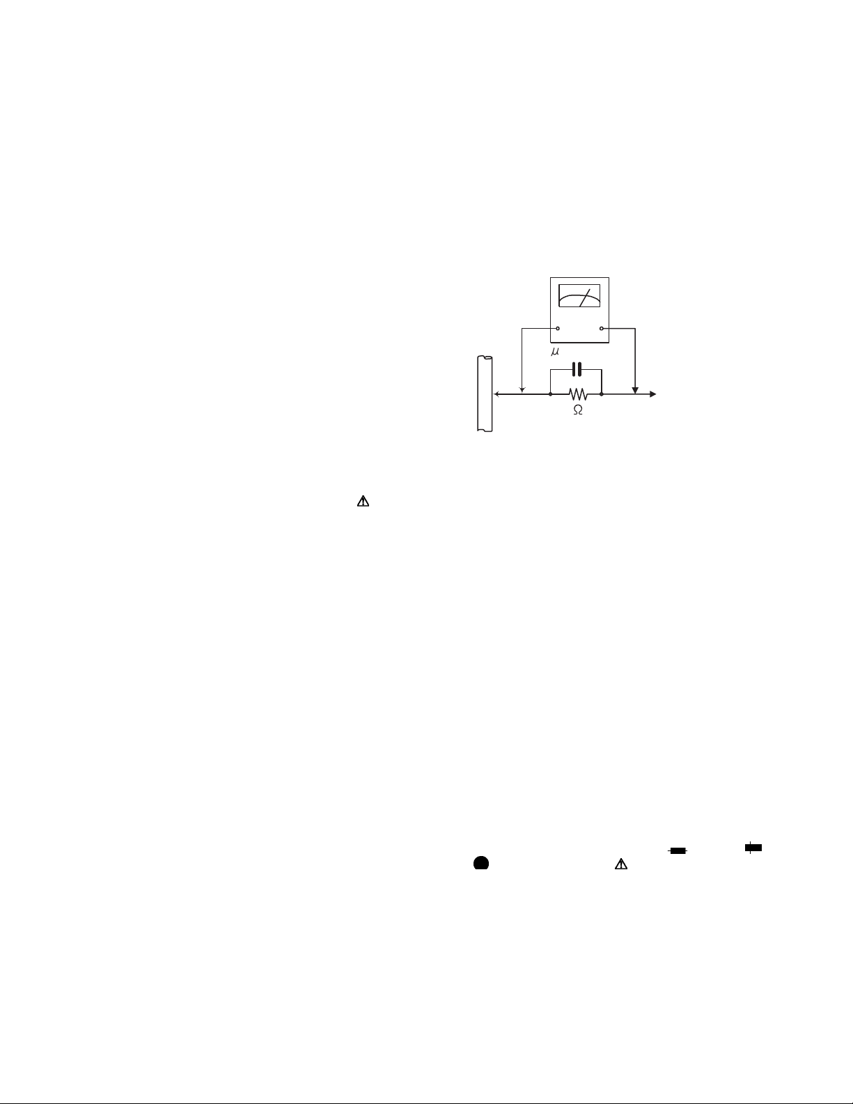
(5) Leakage shock hazard testing
After reassembling the product, always perform an isola-
tion check on the exposed metal parts of the product (an-
tenna terminals, knobs, metal cabinet, screw heads,
headphone jack, control shafts, etc.) to be sure the product
is safe to operate without danger of electrical shock.Do not
use a line isolation transformer during this check.
• Plug the AC line cord directly into the AC outlet. Using a
"Leakage Current Tester", measure the leakage current
from each exposed metal parts of the cabinet, particular-
ly any exposed metal part having a return path to the
chassis, to a known good earth ground. Any leakage cur-
rent must not exceed 0.5mA AC (r.m.s.).
• Alternate check method
Plug the AC line cord directly into the AC outlet. Use an
AC voltmeter having, 1,000Ω per volt or more sensitivity
in the following manner. Connect a 1,500Ω 10W resistor
paralleled by a 0.15µF AC-type capacitor between an ex-
posed metal part and a known good earth ground.
Measure the AC voltage across the resistor with the AC
voltmeter.
Move the resistor connection to each exposed metal
part, particularly any exposed metal part having a return
path to the chassis, and measure the AC voltage across
the resistor. Now, reverse the plug in the AC outlet and
repeat each measurement. Voltage measured any must
not exceed 0.75 V AC (r.m.s.). This corresponds to 0.5
mA AC (r.m.s.).
1.2 Warning
(1) This equipment has been designed and manufactured to
meet international safety standards.
(2) It is the legal responsibility of the repairer to ensure that
these safety standards are maintained.
(3) Repairs must be made in accordance with the relevant
safety standards.
(4) It is essential that safety critical components are replaced
by approved parts.
(5) If mains voltage selector is provided, check setting for local
voltage.
1.3 Caution
Burrs formed during molding may be left over on some parts
of the chassis.
Therefore, pay attention to such burrs in the case of pre-
forming repair of this system.
1.4 Critical parts for safety
In regard with component parts appearing on the silk-screen
printed side (parts side) of the PWB diagrams, the parts that are
printed over with black such as the resistor ( ), diode ( )
and ICP ( ) or identified by the " " mark nearby are critical
for safety. When replacing them, be sure to use the parts of the
same type and rating as specified by the manufacturer.
(This regulation dose not Except the J and C version)
Good earth ground
Place this
probe on
each exposed
metal part.
AC VOLTMETER
(Having 1000
ohms/volts,
or more sensitivity)
1500 10W
0.15 F AC TYPE
(No.MB504)1-5
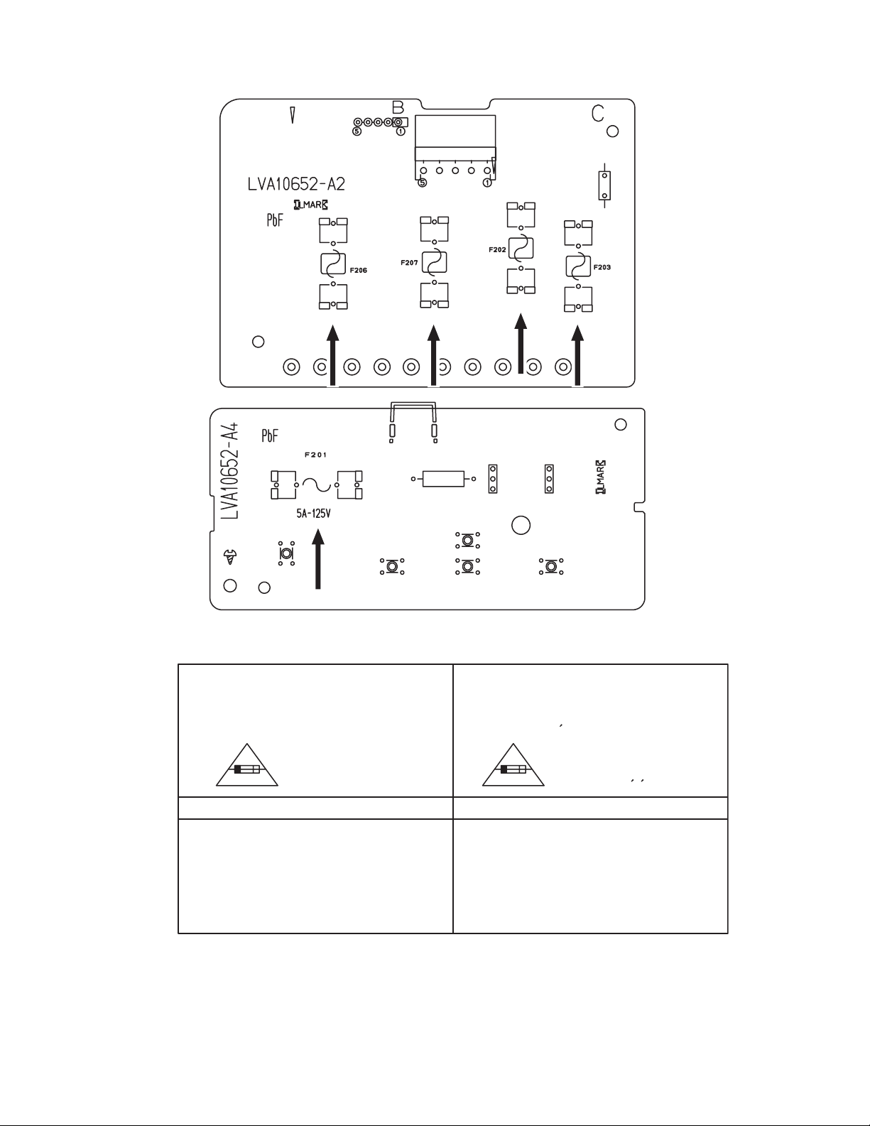
1.5 Importance administering point on the safety
Graphic symbol mark
(This symbol means fast blow type fuse.)
FOR CONTINUED PROTECTION AGAINST RISK
OF FIRE, REPLACE ONLY WITH SAME TYPE
AND RATING OF FUSES ;
should be read as follows ;
F201,F206,F207: 5A 125V
F202,F203 : 2A 125V
F201,F206,F207: 5A 125V
F202,F203 : 2A 125V
Full Fuse Replacement Marking
FUSE CAUTION
Le symbole graphique (Ce symbole signifie
fusible de type a fusion rapide.)
POUR UNE PROTECTION CONTINUE CONTRE
DES RISQUES D'INCENDIE, REMPLACER
SEULEMENT PAR UN FUSIBLE DU MEME TYPE ;
Marquage Pour Le Remplacement
Complet De Fusible
PRECAUTIONS SUR LES FUSIBLES
doit etre interprete comme suit ;
^
CN251
FC272
FC221
FC222
FC231
FC232
FW201
R201
FC261
110 111112 113114 120121 122130 131
FC262
FC271
FC211
FC212
R1
EP1
B106
B105
B104
TA201TA202
PW104
PW102
PW105
PW103
PW101
B103
B102
B101
B108
B107
B109
B110

1-6 (No.MB504)
SECTION 2
SPECIFIC SERVICE INSTRUCTIONS
This service manual does not describe SPECIFIC SERVICE INSTRUCTIONS.
(No.MB504)1-7
SECTION 3
DISASSEMBLY
3.1 Main body
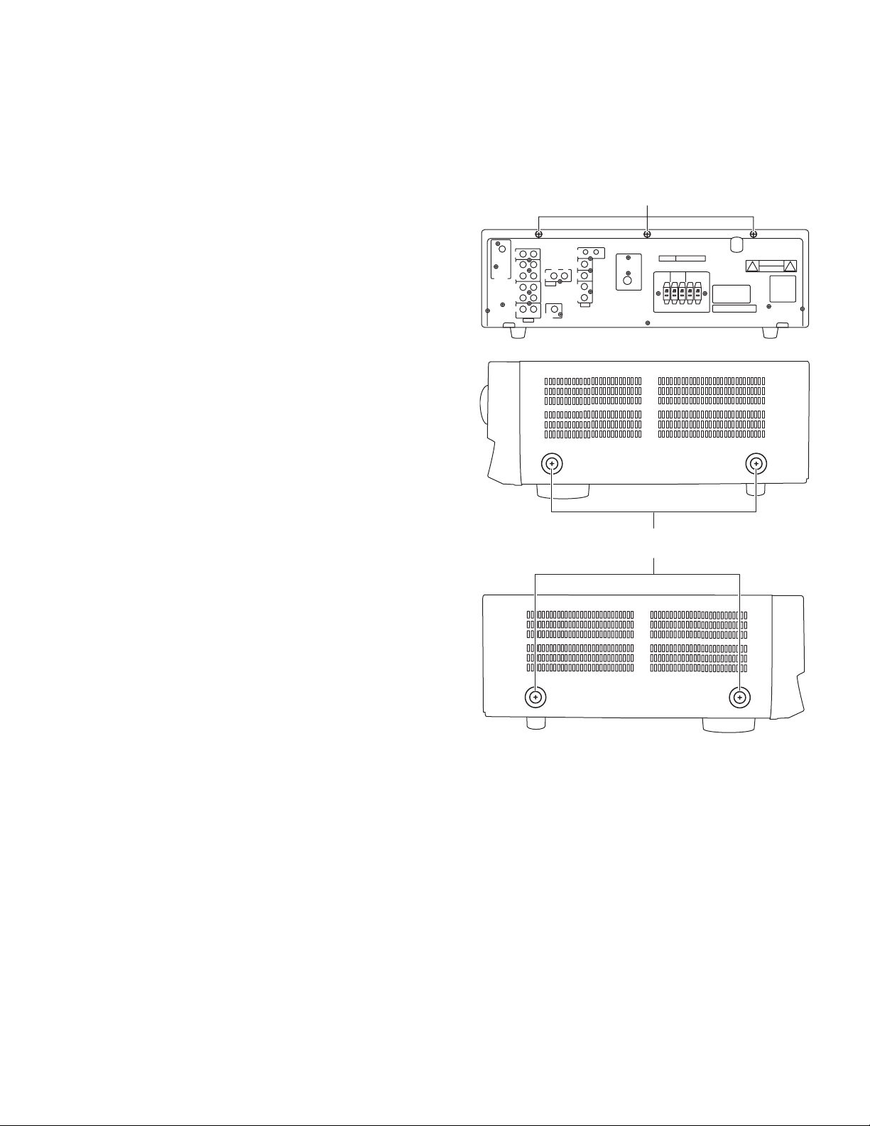
3.1.1 Removing the top cover
(See Fig. 1 and 2)
(1) Remove the three screws A attaching the top cover.
(2) Remove the four screws B attaching the both side of top
cover.
Fig.1
Fig.2
A
B
1-8 (No.MB504)
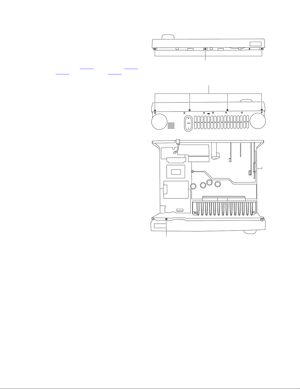
3.1.2 Removing the front panel assembly
(See Fig. 3 to 5)
(1) Remove the three screws C attaching the top side of front
panel assembly.
(2) Remove the four screws D attaching the bottom side of
front panel assembly.
(3) Remove the one screw E attaching the ground wire to front
chassis.
(4) Disconnect the connector to CN404
of audio board, CN504
of video board, CN402 of main board and CN201 of regu-
lator board.
Fig.3
Fig.4
Fig.5
C
D
E
CN504
CN404
CN402
CN201
Regulator board
Main board
(No.MB504)1-9
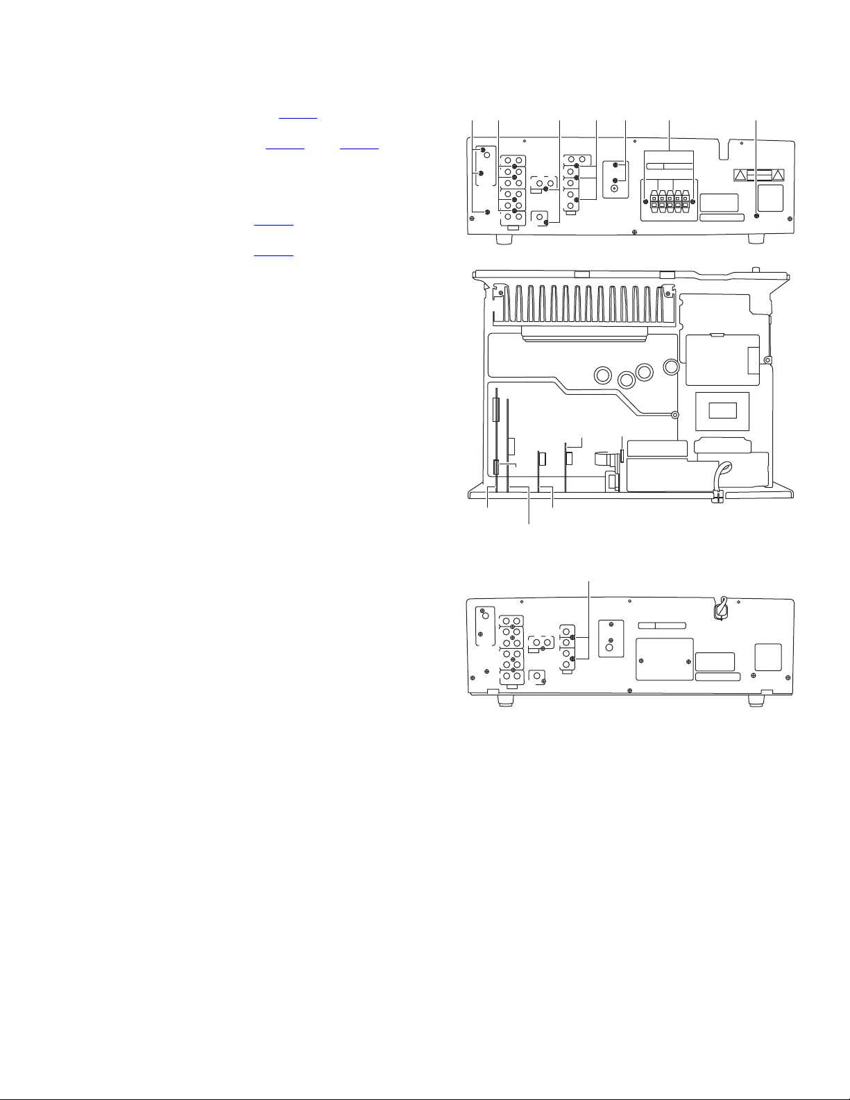
3.1.3 Removing the rear panel and each I/O boards
(See Fig. 6 to 8)
(1) Remove the two screws F attaching the tuner board.
(2) Disconnect the card wire from CN411
of main board.
(3) Remove the three screws G attaching the digital board.
(4) Disconnect the connector CN481
and CN482 of main
board.
(5) Remove the four screws H attaching the main board and
remove the one screw J attaching the ground wire to front
board.
(6) Disconnect the connector CN421
of main board.
(7) Remove the two screws K attaching the subwoofer board.
(8) Disconnect the connector CN431
of main board.
(9) Remove the three screws L attaching the video board (for
European model, two screws L see Fig. 8)
(10) Remove the two screws M attaching the speaker terminal
board.
(11) Remove the one screw N attaching the fuse board.
(12) Remove the three screws P attaching the rear panel.
Fig.6
Fig.7
Fig.8
G FKJH L M
CN481
CN482
CN421
CN431
CN441
CN411
Digital board
Audio board
Subwoofer board
Tun er
Video board
K
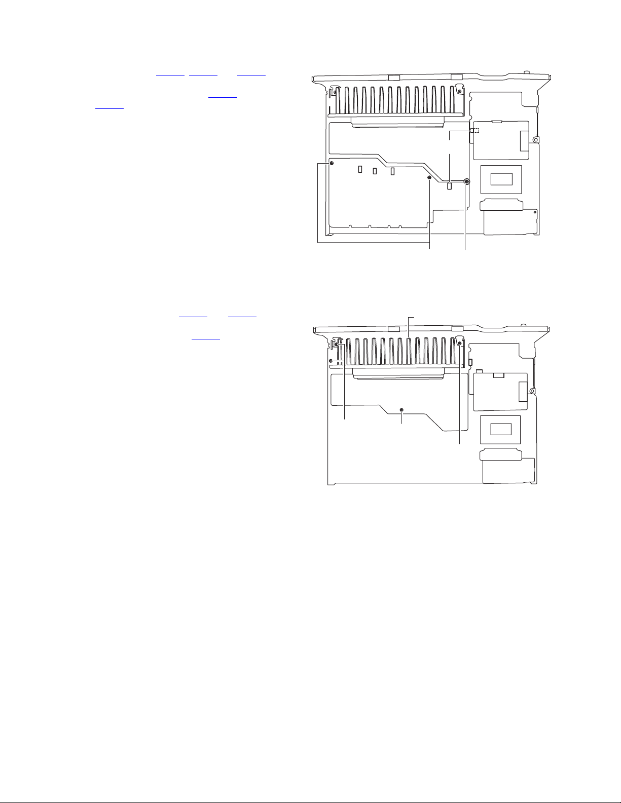
1-10 (No.MB504)
3.1.4 Removing the main board
(See Fig. 9)
(1) Disconnect the connector CN471
, CN472 and CN473 from
front board.
(2) Disconnect the connection board from CN291
of regulator
board and CN491
of main board.
(3) Remove the two screws Q and one screw R attaching the
main board.
Fig.9
3.1.5 Removing the front board and heat sink
(See Fig. 10)
(1) Disconnect the connector from CN203
and CN241 of reg-
ulator board.
(2) Disconnect the connector from CN251 of transformer
board.
(3) Remove the four screws S attaching the heat sink.
(4) Remove the one screw T attaching the front board.
Fig.10
CN491
CN291
R
Q
CN471
CN472
Main board
Regulator board
Connection
board
CN473
CN241
CN203
CN251
Trans board
Regulator
board
Front board
Heat sink
T
S
S

(No.MB504)1-11
3.1.6 Removing the power transformer and regulator board
(See Fig. 11 and 12)
(1) Remove the four screws U attaching the power transform-
er.
(2) Remove the one screw V attaching the fuse board.
(3) Remove the three screws W and one screw X attaching the
regulator board.
(4) Disconnect the wire from CN101
of headphone board.
Fig.11
Fig.12
3.1.7 Removing the headphone board
(See Fig. 13)
(1) Remove the nut Y attaching the head phone board.
Fig.13
V
U
U
Fuse board
Power trans
CN101
W
WX
Regulator board
Headphone jack
Y
1-12 (No.MB504)
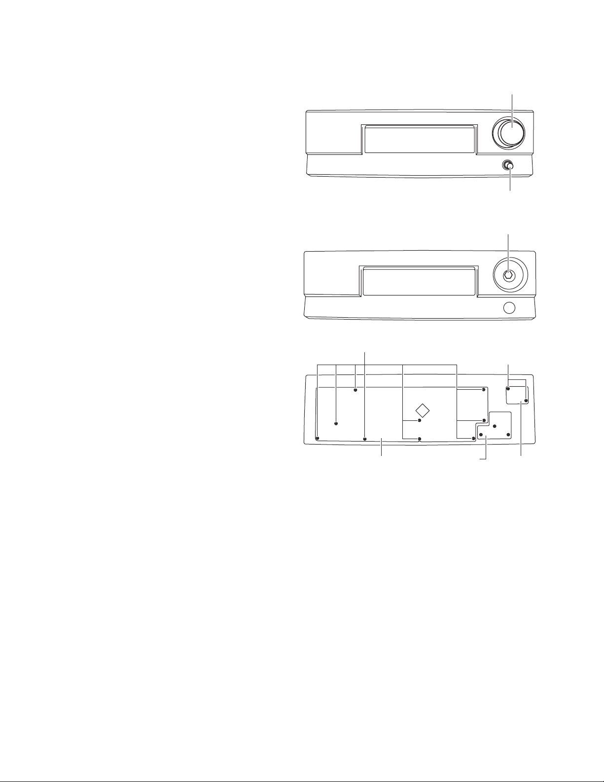
3.2 Front panel assembly
3.2.1 Removing the micon board
(See Fig. 14 and 16)
(1) Take out the volume knob from front panel assembly.
(2) Remove the nut Z attaching the volume.
(3) Remove the nine screws AA attaching the micon board.
3.2.2 Removing the power switch board
(See Fig. 15)
(1) Remove the two screws BB attaching the power switch
board.
3.2.3 Removing the AUX board
(See Fig. 14 and 16)
(1) Take out the multi jog knob from front panel assembly.
(2) Remove the three screws CC attaching the AUX board.
Fig.14
Fig.15
Fig.16
Volume knob
Multi jog knob
Z
AA
BB
Power switch
board
Micon board Aux board

(No.MB504)1-13
SECTION 4
ADJUSTMENT
This service manual does not describe ADJUSTMENT.
SECTION 5
TROUBLESHOOTING
This service manual does not describe TROUBLESHOOTING.

(No.MB504)
Audio/Video Systems Category 10-1,1chome,Ohwatari-machi,Maebashi-city,371-8543,Japan
Victor Company of Japan, Limited
VPT
Printed in Japan
SCHEMATIC DIAGRAMS
RX-5060BJ,RX-5060BC,RX-5060BE
RX-5062SB,RX-5062SE,RX-5062SEN
RX-5062SEV
Contents
Block diagrams
Standard schematic diagrams
Printed circuit boards
2-1
2-3
2-15 to 21
CD-ROM No.SML200602
AUDIO/VIDEO CONTROL RECEIVER
No.MB504SCH
2006/2
COPYRIGHT 2006 Victor Company of Japan, Limited.
Lead free solder used in the board (material : Sn-Ag-Cu, melting point : 219 Centigrade)
TA/NEWS/INFO
DISPLAY MODE

In regard with component parts appearing on the silk-screen printed side (parts side) of the PWB diagrams, the
parts that are printed over with black such as the resistor ( ), diode ( ) and ICP ( ) or identified by the " "
mark nearby are critical for safety.

< MEMO >
2-1
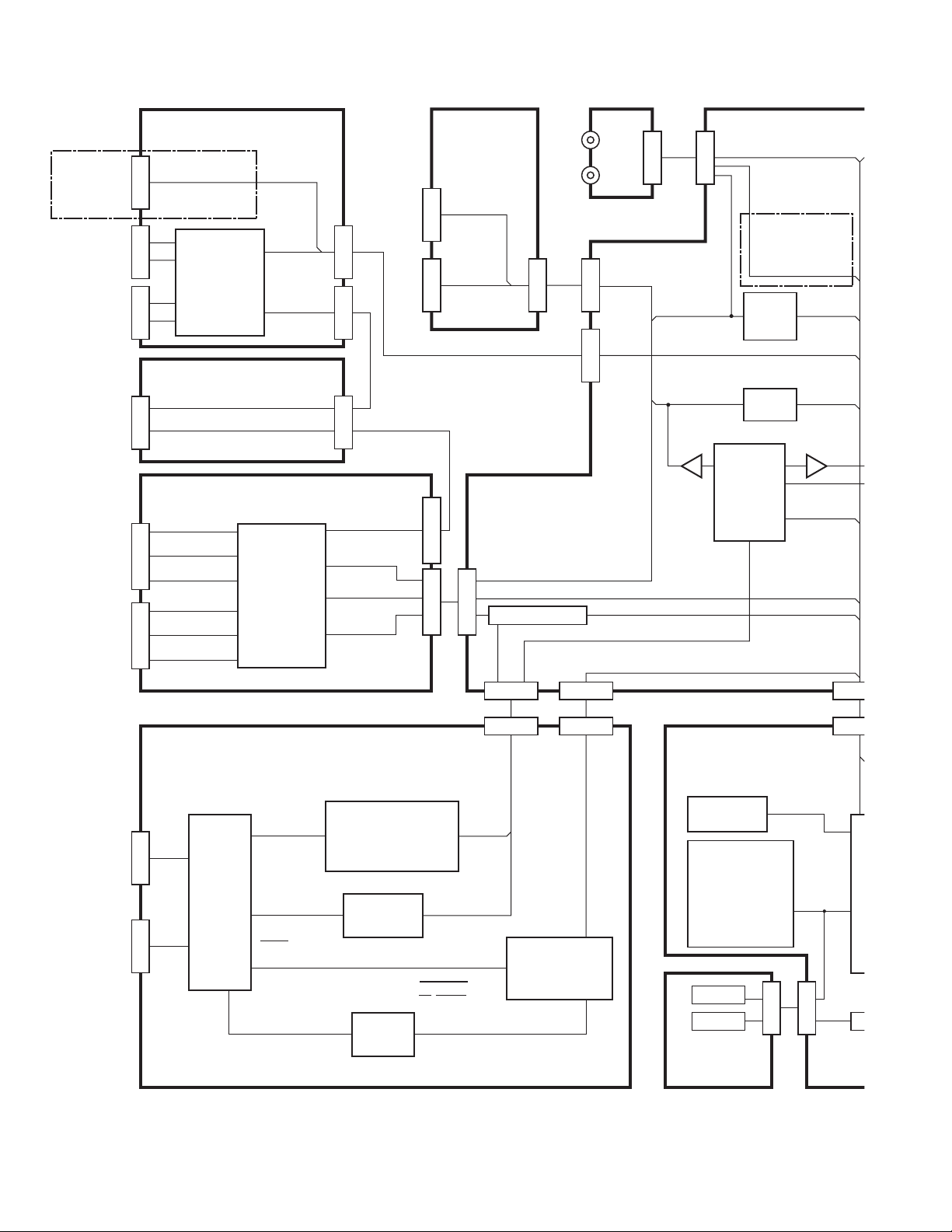
Q
Tune r
DSP_CLK,DSP_STATUS,DSP_READY
DSP_RESET,DSP_COMMAND
VOL_CLK
VOL_DA
KEY_IN1
KEY_IN2
KEY_IN3
KEY_IN4
KEY_IN5
CN411
CN481
AM
FM
DSP_L/R,DSP_SL/SR
DSP_C,DSP_LFE
IC402
SOURCE
SELECTOR
IC428
6CH
MASTER
VOLUME
C
DI701
FL DISPLAY
CN401CN404
VCROUT_L/R
CD_L/R
VCRIN_L/R
TV_L/R
TAPEOUT_L/R
TAPEIN_L/R
SIG_L/R
TUNER_L/R
DVD_L/R
AUX_L/R
DVD_L/R
SW_OUT
SW_OUT
J406
DVD
J404
J402
CD
TAPE_PLAY
TAPE_REC
J403
TV_SOUND
VCR_PLAY
VCR_REC
CN431
INPUT_ATT
CN482
CN
4
CN
7
SW_OUT
DVD_L/R
DIGITAL IN1
J681
DIGITAL IN2
UN682
IC601,IC602
FILTER
IC661
DSP
IC667
CODEC
with
S/PDIF
IC611,IC612,IC613
IC615,IC622,IC631
IC632,IC633,IC634
FILTER
IC671
DSP, CODEC
CONTROLLER
LIN+/-
RIN+/-
A1+/-,B1+/-
A2+/-,B2+/-
A3+/-,B3+/-
CN683
CN681
S727
D719
CN714
CN704
KEY_IN
S721 to S726
S728 to S732
S734 to S736
S738,S739
S740 to S743
S745,S746
S750 to S752
SEG1 to 16
GRID1 to 16
RX0
RX1
Power switch
section
User control keys /
System control LSI /
FL display section
Surround IC / Digital signal
input terminal section
CN451
TU_DATAIN
TU_DATAOUT
TU_CLK
TU_CE
CN441
Audio/Video signal input terminal section
(Audio)
TUNER_L
TUNER_R
Audio/Video
signal input
terminal
section (DVD)
Volume / Regulator / S
o
SW_DATA
SW_CLK
SW_DATA, SW_CLK
TU_MUTE
IN_L/R
CN421
Q1421 to Q1423
S
_
DSP_IN_L/R
DSP.L
DSP.R
DSP.LS
DSP.RS
DSP.C
DSP.SW
CDIN,CDOUT
CCLK,INT
D_RST,D_CS
D/A0 to D/A3
DATA,MCK,XTAL
S_BCK,S_LRCK
C_BCK,C_LRCK
DSP_RST
SS,HREQ
MOSI,MISO
GPIO1 to GPIO4
SW_OUT
S_MUTE
SW_MUTE
Q1424
Q1426
Q1427
Q1428
Q1429
IC427 IC422
CN904
Audio/Video signal input
terminal section (Aux)
AUX_L/R
AUX_VIDEO
J901
AUX
VIDEO
L
R
Block diagram
RDS_CLK
RDS_DATA
RDS_ONOFF
For B/E/EN/EV
AUX_VIDEO
CN504
Audio/Video signal input
terminal section (Video)
IC501
SELECTOR
J501
DVD
MONITOR
CN501
VIDEO1
VIDEO2
P
R
J502
VCR1
J521
COMPULINK
COMPULINK
For J/C
 Loading...