


 Loading...
HP MSA-2011, MSA-2086-TR1, MSA-2086, MSA-2085, MSA-2035 Datasheet
...Silicon Bipolar RFIC Amplifiers
Technical Data
Features
MSA-2011
•Surface Mount SOT-143 Package
•3 dB Bandwidth:
DC to 1.0 GHz
•16.2 dB Gain at 1 GHz
•4.3 dB NF at 1 GHz
MSA-2035
•Hermetic Ceramic Package
•3 dB Bandwidth:
DC to 1.1 GHz
•17.3 dB Gain at 1 GHz
•3.7 dB NF at 1 GHz
MSA-2085
•Plastic Microstrip Package
•3 dB Bandwidth:
DC to 1.1 GHz
•16.6 dB Gain at 1 GHz
•3.7 dB NF at 1 GHz
MSA-2086
•Surface Mount Plastic Microstrip Package
•3 dB Bandwidth:
DC to 1.1 GHz
•16.6 dB Gain at 1 GHz
•3.7 dB NF at 1 GHz
MSA-2011
MSA-2035
MSA-2085
MSA-2086
MSA-20XX Series
Description
The MSA-20XX series are high performance silicon bipolar RFIC amplifiers designed to be cascadable in 50 Ω systems. The stability factor of K > 1 contributes to easy cascading in numerous narrow and broadband IF and RF commercial and industrial applications.
The MSA series is fabricated using
a 10 GHz fT, 25 GHz FMAX, silicon bipolar RFIC process which
utilizes nitride self-alignment, ion implantation, and gold metallization to achieve excellent uniformity, performance, and reliability. The use of an external bias resistor for temperature and current stability also allows bias flexibility.
Package options include the industry standard plastic surface mount SOT-143 package, the 100Ê mil surface mountable hermetic ceramic package, the 85Ê mil plastic microstripline package, and the 85 mil surface mountable plastic microstripline package.
5965-9560E |
6-470 |
Absolute Maximum Ratings[1]
|
MSA- |
MSA- |
MSA- |
Parameter |
2011 |
2035 |
2085, -2086 |
|
|
|
|
Device Current |
50 mA |
60 mA |
60 mA |
|
|
|
|
Power Dissipation[2,3] |
250mW[3a] |
325mW[3b] |
325mW[3c] |
RF Input Power |
+13dBm |
+13dBm |
+13dBm |
|
|
|
|
Junction |
150°C |
200°C |
150°C |
Temperature |
|
|
|
|
|
|
|
Storage Temperature |
-65 to 150°C |
-65 to 200°C |
-65 to 150°C |
|
|
|
|
|
|
|
|
Thermal |
500°C/W |
155°C/W |
115°C/W |
Resistance: θjc |
|
|
|
|
|
|
|
Notes:
1.Permanent damage may occur if any of these limits are exceeded.
2.TCASE = 25°C.
3a. Derate at 2.0 mW/°C for TC > 25°C.
b.Derate at 6.5 mW/°C for TC > 149°C.
c.Derate at 8.7 mW/°C for TC > 112°C.
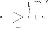
Typical Biasing
Configuration
Rbias
VCC ≥ 7 V
|
4 |
|
|
|
|
|
|
|
RF CHOKE |
|||||||||
|
|
|
|
|
|
|
|
|||||||||||
|
|
|
|
|
|
|
|
|||||||||||
|
|
|
|
|
|
|
|
|||||||||||
|
|
|
|
|
|
|
|
|
|
|
|
|
|
|||||
|
DC BLOCK |
|
|
3 |
|
|
|
|
|
|
||||||||
INPUT |
|
|
|
|
MSA |
|
|
|
|
OUTPUT |
||||||||
|
|
|
|
|
|
|||||||||||||
|
|
|
1 |
|
|
|
|
|
|
|
|
|
|
|||||
|
|
|
|
2 |
|
|
|
|
|
|
|
Vd = 5 V |
||||||
|
|
|
|
|
|
|||||||||||||
|
|
|
|
|
|
|
|
|
|
|
|
Rbias = VCC – Vd |
||||||
|
|
|
|
|
|
|
|
|
|
|
|
|
||||||
|
|
|
|
|
|
|
|
|
|
|
|
|
||||||
|
|
|
|
|
|
|
|
|
|
|
|
|
|
|
|
I d |
|
|
Electrical Specifications, TA = 25°C
ID = 32 mA, Zo = 50 Ω
|
Parameters and |
|
MSA-2011 |
|
MSA-2035 |
MSA-2085, -2086 |
||||||
|
|
|
|
|
|
|
|
|
|
|
|
|
|
|
|
|
|
|
|
|
|
|
|
|
|
Symbol |
Test Conditions |
Units |
Min. |
Typ. |
Max. |
Min. |
|
Typ. |
Max. |
Min. |
Typ. |
Max. |
|
|
|
|
|
|
|
|
|
|
|
|
|
GP |
Power Gain |
|
|
|
|
|
|
|
|
|
|
|
|
(|S21|2) |
dB |
|
18.9 |
|
17.8 |
|
19.2 |
19.8 |
|
19.2 |
|
|
f = 0.1 GHz |
|
|
|
|
|
||||||
|
f = 0.5 GHz |
|
|
18.1 |
|
|
|
18.7 |
|
|
18.3 |
|
|
f = 1.0 GHz |
|
15.0 |
16.2 |
|
|
|
17.3 |
|
15.0 |
16.6 |
|
|
|
|
|
|
|
|
|
|
|
|
|
|
GP |
Gain Flatness |
|
|
± 0.6 |
|
|
|
± 0.4 |
± 1.0 |
|
± 0.6 |
|
|
f = 0.1 to 0.6 GHz |
dB |
|
|
|
|
|
|
||||
f3dB |
3 dB Bandwidth |
GHz |
|
1.0 |
|
|
|
1.1 |
|
|
1.1 |
|
VSWR |
Input VSWR |
|
|
|
|
|
|
|
|
|
|
|
|
f = 0.1 to 3.0 GHz |
|
|
1.3:1 |
|
|
|
1.3:1 |
|
|
1.2:1 |
|
|
|
|
|
|
|
|
|
|
|
|
|
|
|
Output VSWR |
|
|
|
|
|
|
|
|
|
|
|
|
f = 0.1 to 3.0 GHz |
|
|
1.4:1 |
|
|
|
1.4:1 |
|
|
1.5:1 |
|
|
|
|
|
|
|
|
|
|
|
|
|
|
P1dB |
Power Output @ |
|
|
|
|
|
|
|
|
|
|
|
|
1 dB Gain |
|
|
|
|
|
|
|
|
|
|
|
|
Compression: |
|
|
|
|
|
|
|
|
|
|
|
|
f = 1.0 GHz |
dBm |
|
9.0 |
|
|
|
9.5 |
|
|
9.0 |
|
|
|
|
|
|
|
|
|
|
|
|
|
|
NF |
50 Ω Noise Figure |
|
|
|
|
|
|
|
|
|
|
|
|
f = 1.0 GHz |
dB |
|
4.3 |
|
|
|
3.7 |
|
|
3.7 |
|
IP3 |
Third Order |
|
|
|
|
|
|
|
|
|
|
|
|
Intercept |
|
|
|
|
|
|
|
|
|
|
|
|
Point |
|
|
|
|
|
|
|
|
|
|
|
|
f = 1.0 GHz |
dBm |
|
22 |
|
|
|
22 |
|
|
22 |
|
|
|
|
|
|
|
|
|
|
|
|
|
|
td |
Group Delay |
psec |
|
143 |
|
|
|
143 |
|
|
143 |
|
|
f = 1.0 GHz |
|
|
|
|
|
|
|
||||
VD |
Device Voltage |
|
|
|
|
|
|
|
|
|
|
|
|
TC = 25°C |
V |
4.0 |
5.0 |
6.0 |
4.5 |
|
5.0 |
5.5 |
4.3 |
5.0 |
6.3 |
dV/dT |
Device Voltage |
mV/°C |
|
|
|
|
|
|
|
|
|
|
|
Temperature |
|
-9.3 |
|
|
|
-9.3 |
|
|
-9.3 |
|
|
|
Coefficient |
|
|
|
|
|
|
|
|
|
|
|
|
|
|
|
|
|
|
|
|
|
|
|
|
Note: |
|
|
|
|
|
|
|
|
|
|
|
|
1. Refer to “Tape and Reel Packaging for Surface Mount Devices.” |
|
|
|
|
|
|
|
|
|
|||
6-471

Typical Performance for MSA-2011
|
25 |
|
|
|
20 |
|
|
|
|
|
|
|
|
|
19 |
|
0.1 GHz |
|
|
|
|
|
|
|
|
|
|
|
|
|
20 |
|
-55°C |
|
18 |
|
|
|
|
|
|
|
|
|
|
|
|
||
|
|
|
-25°C |
|
17 |
|
0.5 GHz |
|
|
(dB)Gp |
|
|
25°C |
(dB)GAIN |
16 |
|
|
|
|
15 |
|
85°C |
|
1.0 GHz |
|
|
|||
|
|
|
|
|
|
||||
|
|
|
15 |
|
|
|
|||
|
|
|
|
|
|
|
|
|
|
|
|
|
|
|
14 |
|
|
|
|
|
10 |
|
|
|
13 |
|
|
|
|
|
|
|
|
|
|
|
|
|
|
|
|
|
|
|
12 |
|
2.0 GHz |
|
|
|
|
|
|
|
|
|
|
|
|
|
5 |
|
|
|
11 |
|
|
|
|
|
0.1 |
1.0 |
4.0 |
|
20 |
25 |
30 |
35 |
40 |
|
|
FREQUENCY (GHz) |
|
|
|
|
I d (mA) |
|
|
P 1dB(dBm)
16 |
|
|
|
14 |
40 mA |
|
|
|
|
|
|
12 |
35 mA |
|
|
|
|
|
|
10 |
30 mA |
|
|
|
|
|
|
8 |
|
|
|
|
25 mA |
|
|
6 |
|
|
|
4 |
20 mA |
|
|
|
|
|
|
2 |
|
|
|
0 |
|
|
|
|
0.1 |
1.0 |
4.0 |
FREQUENCY (GHz)
Figure 1. Power Gain vs. Frequency at |
Figure 2. Power Gain vs. Current at |
Figure 3. Typical P1dB vs. Frequency at |
Four Temperatures, ID = 32 mA. |
25°C. |
25°C. |
(dB) |
6 |
|
|
|
|
|
|
|
|
|
|
|
|
|
|
|
|
|
|
|
|
|
|
|
|
|
|
|
|
|
|
||
5 |
|
|
|
|
|
|
|
|
|
|
|
|
|
|
|
|
|
|
|
|
|
|
|
|
|
|
|
|
|
|
|
||
FIGURE |
|
|
|
|
|
|
|
|
|
|
|
|
|
|
|
|
|
|
|
|
|
|
|
|
|
|
40 mA |
|
|
|
|
|
|
NOISE |
4 |
|
|
|
|
|
|
|
|
|
|
|
|
|
|
|
|
|
|
|
|
|
|
|
|
|
20 mA |
|
|
||||
|
|
|
|
|
|
|
|
|
|
|
|
|
|
|||
|
3 |
|
|
|
|
|
|
|
|
|
|
|
|
|
|
|
|
|
|
|
|
|
|
|
|
|
|
|
|
|
|
|
|
|
|
|
|
|
|
|
|
|
|
|
|
|
|
|
|
|
|
0.1 |
1.0 |
4.0 |
|||||||||||||
FREQUENCY (GHz)
Figure 4. Noise Figure vs. Frequency at ID = 32 mA.
(dB) |
17 |
|
|
|
|
|
|
|
|
|
|
|
|
|
GP |
|
|
|
|
|
|||
|
|
|
|
|
|
|
|
|
|||
GAIN |
16 |
|
|
|
|
|
|
|
|
6 |
|
|
|
|
|
|
|
|
|
|
|||
15 |
|
|
|
|
|
|
|
|
(dB) |
||
|
|
|
|
|
|
|
|
|
|
5 |
FIGURE |
|
|
|
|
|
|
|
|
|
|
|
|
|
|
|
|
|
|
|
|
|
|
|
|
|
|
|
|
|
NF |
|
|
|
|
|
|
(dBm) |
10 |
|
|
|
|
|
|
|
|
4 |
NOISE |
|
|
P1dB |
|
|
|
||||||
9 |
|
|
|
|
|
3 |
|||||
|
|
|
|
|
|
|
|
|
|||
1dB |
|
|
|
|
|
|
|
|
|
|
|
P |
8 |
|
|
|
|
|
|
|
|
|
|
|
|
|
|
|
|
|
|
|
|
|
|
|
7 |
|
|
|
|
|
|
|
|
|
|
|
|
|
|
|
|
|
|
|
|
|
|
|
-25 |
25 |
85 |
|
|||||||
AMBIENT TEMPERATURE (°C)
Figure 5. Power Gain, Noise Figure,
and P1dB vs. Temperature at 1 GHz and ID = 32 mA.
|
40 |
|
|
-55°C |
|
|
|
|
|
|
|
|
|
|
|
|
|
|
|
-25°C |
|
|
|
|
30 |
|
|
25°C |
|
|
|
|
|
|
85°C |
|
|
|
|
|
|
|
|
|
|
|
|
mA |
20 |
|
|
|
|
|
|
D |
|
|
|
|
|
|
|
I |
|
|
|
|
|
|
|
|
10 |
|
|
|
|
|
|
|
0 |
|
|
|
|
|
|
|
0 |
1 |
2 |
3 |
4 |
5 |
6 |
VD (VOLTS)
Figure 6. ID vs. VD at Four
Temperatures.
6-472
Loading...