


K4D263238A-GC50
Samsung K4D263238A-GC50, K4D263238A-GC45, K4D263238A-GC40, K4D263238A-GC36, K4D263238A-GC33 Datasheet
K4D263238A-GC
128Mbit DDR SDRAM
Double Data Rate Synchronous DRAM
with Bi-directional Data Strobe and DLL
128M DDR SDRAM
1M x 32Bit x 4 Banks
(144-Ball FBGA)
Revision 2.0
January 2003
Samsung Electronics reserves the right to change products or specification without notice.
- 1 -
Rev. 2.0 (Jan. 2003)

K4D263238A-GC
128M DDR SDRAM
Revision History
Revision 2.0 (January 16, 2002)
• Changed package ball height from 0.25mm to 0.35mm
• Typo corrected
Revision 1.9 (July 18, 2002)
• Changed power dissipation from 2.0W to 2.3W
Revision 1.8 (June 12, 2002)
• Supported both CL4 and CL3 for the K4D263238A-GC45 and the effective date of this change starts from WW23
Revision 1.6 (January 30, 2002)
• Changed tCK(max) of K4D263238A-GC40 from 7ns to 10ns.
• Changed tCK(max) of K4D263238A-GC33/36 from 5ns to 4ns. For all the CL5 operation, guaranteed tCK(max) is 4ns.
Revision 1.5 (December 14, 2001)
• Removed K4D26323RA-GC2A/33/36(VDD/VDDQ=2.8V) & K4D263238A-GC55/60 from the spe c.
• Added K4D263238A-GC36(VDD/VDDQ=2.5V)
Revision 1.4 (November 14, 2001)
• Added K4D26323RA-GC36(VDD/VDDQ=2.8V)
Revision 1.3 (October 22, 2001)
• Corrected part number of K4D263238A-GC2A to K4D26323RA-GC2A
• Changed tCDLR of -GC2A and GC33 from 3tCK to 2tCK and applied since Sept 15, 2001.
• Defined x32 DDR for mobile PC graphics separately - K4D26323AA-GL** featured with VDDQ=1.8V,ICC6=1mA with
reduced operating current. Refer to the K4D26323AA-GL** spec for more detail information.
Revision 1.2 (September 13, 2001)
• Define DC spec value of K4D26323RA-GC33 and K4D263238A-GC2A
• Changed tCK(max) of -2A and -33 from 7ns to 5ns
Revision 1.1 (September 3, 2001)
• Added K4D26323RA-GC33(VDD/VDDQ=2.8V)
• Added K4D263238A-GC2A(350MHz)
Revision 1.0 (August 16, 2001)
• Changed tCDLR of K4D263238A-GC33 from 2tCK to 3tCK
• Removed VDDQ=1.8V from the spec.
• Added K4D263238A-GL as a low power part
• Defined DC spec.
Revision 0.1 (August 2, 2001) - Target Spec
• Changed tCK(max) of K4D263238A-GC45/-50/-55/-60 from 7ns to 10ns.
Revision 0.0 (June, 2001) - Target Spec
• Defined Target Specification
- 2 -
Rev. 2.0 (Jan. 2003)
K4D263238A-GC
1M x 32Bit x 4 Banks Double Data Rate Synchronous DRAM
with Bi-directional Data Strobe and DLL
FEATURES
• 2.5V +
• 2.5V + 5% power supply for I/O interface
• SSTL_2 compatible inputs/outputs
• 4 banks operation
• MRS cycle with address key programs
-. Read latency 3,4,5 (clock)
-. Burst length (2, 4, 8 and Full page)
-. Burst type (sequential & interleave)
• Full page burst length for sequential burst type only
• Start address of the full page burst should be even
• All inputs except data & DM are sampled at the positive
• Differential clock input
• No Wrtie-Interrupted by Read Function
5% power supply for device operation
going edge of the system clock
• 4 DQS’s ( 1DQS / Byte )
• Data I/O transactions on both edges of Data strobe
• DLL aligns DQ and DQS transitions with Clock transition
• Edge aligned data & data strobe output
• Center aligned data & data strobe input
• DM for write masking only
• Auto & Self refresh
• 32ms refresh period (4K cycle)
• 144-Ball FBGA
• Maximum clock frequency up to 300MHz
• Maximum data rate up to 600Mbps/pin
128M DDR SDRAM
ORDERING INFORMATION
Part NO. Max Freq. Max Data Rate Interface Package
K4D263238A-GC33 300MHz 600Mbps/pin
K4D263238A-GC36 275MHz 550Mbps/pin
K4D263238A-GC40 250MHz 500Mbps/pin
K4D263238A-GC45 222MHz 444Mbps/pin
K4D263238A-GC50 200MHz 400Mbps/pin
SSTL_2
(VDD/VDDQ=2.5V) 144-Ball FBGA
GENERAL DESCRIPTION
FOR 1M x 32Bit x 4 Bank DDR SDRAM
The K4D263238A is 134,217,728 bits of hyper synchronous data rate Dynamic RAM organized as 4 x1,048,576 words by
32 bits, fabricated with SAMSUNG’s high performance CMOS technology. Synchronous features with Data Strobe allow
extremely high performance up to 2.4GB/s/chip. I/O transactions are possible on both edges of the clock cycle. Range of
operating frequencies, programmable burst length and pro grammable latencies allow the d evice to be useful for a variety
of high performance memory system applications.
- 3 -
Rev. 2.0 (Jan. 2003)
K4D263238A-GC
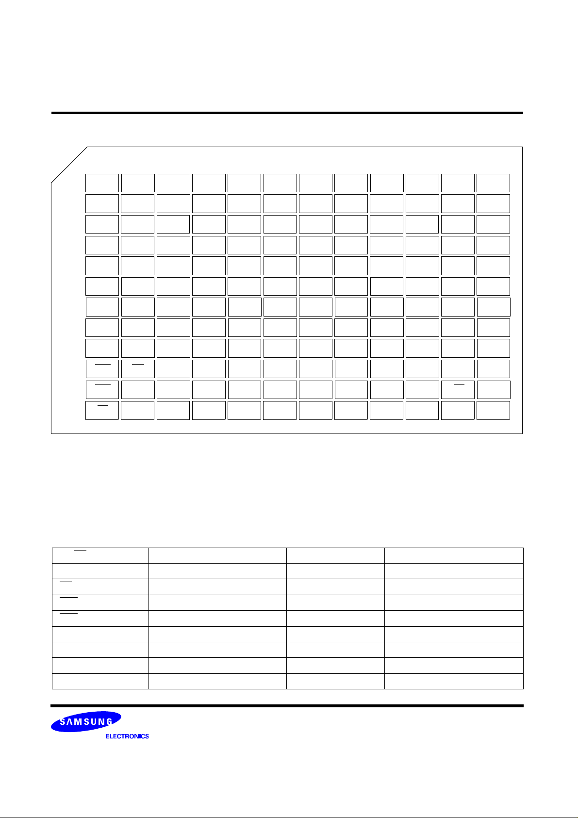
PIN CONFIGURATION (Top View)
2345678910111213
DQS0
B
DM0
VSSQ
DQ3
DQ2
DQ0
DQ31
DQ29
128M DDR SDRAM
DQ28
VSSQ
DM3
DQS3
DQ4
C
DQ6
D
DQ7
E
DQ17
F
DQ19
G
DQS2
H
DQ21
J
DQ22
K
CAS
L
RAS
M
N
CS
VDDQ
DQ5
VDDQ
DQ16
DQ18
DM2
DQ20
DQ23
WE
NC
NC
VSSQ VSSQ VSSQ
VDD
VDDQ
VDDQ
VDDQ
VDDQ
VDD
BA0
NOTE:
1. RFU1 is reserved for A12
2. RFU2 is reserved for BA2
3. VSS Thermal balls are optional
NC
NC
NC
A2
A1
VDDQ
VDD
VSS
Thermal
VSS
Thermal
VSS
Thermal
VSS
Thermal
VDD VDD
A11
A3
VDDQ
VSS VSS VSS VSS
VSSQ
VSSQ
VSSQ
VSSQ
VSSQ
VSS
BA1
A0
DQ1
VSSQ
VSS
Thermal
VSS
Thermal
VSS
Thermal
VSS
Thermal
A10
VDDQ
VDD
VSS
Thermal
VSS
Thermal
VSS
Thermal
VSS
Thermal
A9
A4
DQ30
VSSQ
VSSQ
VSS
Thermal
VSS
Thermal
VSS
Thermal
VSS
Thermal
VSSVSSVSSVSS
RFU
1
A6
VDDQ NC
VSSQ VSSQ
VSSQ
VSSQ
VSSQ
VSSQ
VSSQ
VSS
RFU
A7
VDDQ
DQ26
VDD
VDDQ
VDDQ
NC
VDDQ
VDDQ
VDD
CK
2A5
A8/AP
VDDQ
DQ15
DQ13
DM1
DQ11
DQ9
NC
CK
CKE
DQ27
DQ25
DQ24
DQ14
DQ12
DQS1
DQ10
DQ8
NC
MCL
VREF
PIN DESCRIPTION
CK,CK Differential Clock Input BA0, BA1 Bank Select Address
CKE Clock Enable A0 ~A11 Address Input
CS Chip Select DQ0 ~ DQ31 Data Input/Output
RAS
CAS
WE Write Enable VDDQ Power for DQ’s
DQS Data Strobe VSSQ Ground for DQ’s
DM Data Mask NC No Connection
RFU Reserved for Future Use MCL Must Connect Low
Row Address Strobe VDD Power
Column Address Strobe VSS Ground
- 4 -
Rev. 2.0 (Jan. 2003)
K4D263238A-GC
128M DDR SDRAM
INPUT/OUTPUT FUNCTIONAL DESCRIPTION
Symbol Type Function
The differential system clock Input.
CK, CK*1 Input
CKE Input
CS Input
RAS
CAS Input
WE Input
DQS0 ~ DQS3 Input/Output
DM0 ~ DM3 Input
DQ0 ~ DQ31 Input/Output Data inputs/Outputs are multiplexed on the same pins.
BA0, BA1 Input Selects which bank is to be active.
A0 ~ A11 Input
V
DD/VSS Power Supply Power and ground for the input buffers and core logic.
VDDQ/VSSQ Power Supply
VREF Power Supply Reference voltage for inputs, used for SSTL interface.
NC/RFU No connection/
MCL Must Connect Low Must connect low
*1 : The timing reference point for the differential clocking is the cross point of CK and CK.
For any applications using the single ended clocking, apply V
Input
Reserved for future use
All of the inputs are sampled on the rising edge of the clock except
DQ’s and DM’s that are sampled on both edges of the DQS.
Activates the CK signal when high and deactivates the CK signal
when low. By deactivating the clock, CKE low indicates the Power
down mode or Self refresh mode.
CS enables the command decoder when low an d di sa bl e d th e command decoder when high. When the command decoder is disabled,
new commands are ignored but previous operations continue.
Latches row addresses on the positive going edge of the CK with
RAS
low. Enables row access & precharge.
Latches column addresses on the positive going edge of the CK with
CAS low. Enables column access.
Enables write operation and row precharge.
Latches data in starting from CAS, WE active.
Data input and output are synchronized with both edge of DQS.
DQS0 for DQ0 ~ DQ7, DQS1 for DQ8 ~ DQ15, DQS2 for DQ16 ~ DQ23,
DQS3 for DQ24 ~ DQ31.
Data In mask. Data In is masked by DM Latency=0 when DM is high
in burst write. DM0 for DQ0 ~ DQ7, DM1 for DQ8 ~ DQ15, DM2 for
DQ16 ~ DQ23, DM3 for DQ24 ~ DQ31.
Row/Column addresses are multiplexed on the same pins.
Row addresses : RA0 ~ RA11, Column addresses : CA0 ~ CA7.
Column address CA
Isolated power supply and ground for the output buffers to provide
improved noise immunity.
This pin is recommended to be left "No connection" on the device
REF to CK pin.
8 is used for auto precharge.
- 5 -
Rev. 2.0 (Jan. 2003)
K4D263238A-GC
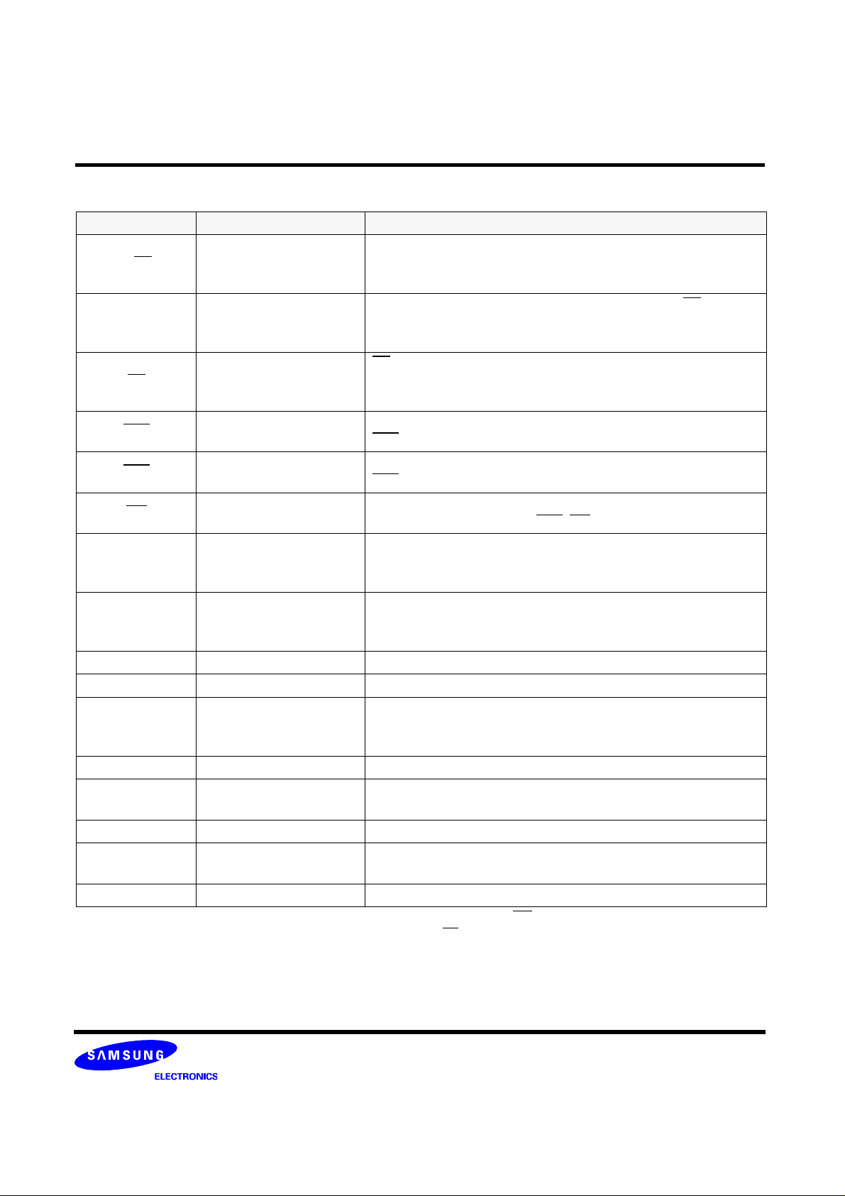
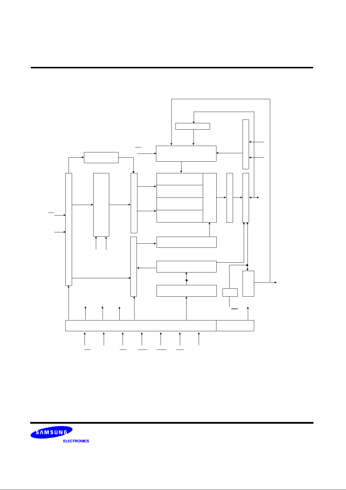
BLOCK DIAGRAM (1Mbit x 32I/O x 4 Bank)
128M DDR SDRAM
32
Intput Buffer
LWE
CK,CK
ADDR
LCKE
Address Register
Bank Select
LRAS
Refresh Counter
Row Buffer
LCBR
LRAS
LCBR
LWE
CK, CK
Row Decoder
Col. Buffer
LCAS
Data Input Register
Serial to parallel
64
1Mx32
1Mx32
1Mx32
1Mx32
Column Decoder
Latency & Burst Length
Programming Register
LWCBR
Sense AMP
2-bit prefetch
64 32
DLL
CK,CK
LDMi
Output BufferI/O Control
x32
DQi
Strobe
Gen.
LDMi
Data Strobe
(DQS0~DQS3)
CK,CK
Timing Register
CKE CS RAS CAS WE DMi
- 6 -
Rev. 2.0 (Jan. 2003)
 Loading...