


 Loading...
ORDER NO.
ARP3468
PLASMA TELEVISION
PDP-508XG
PDP-508XDA
PDP-508XC
THIS MANUAL IS APPLICABLE TO THE FOLLOWING MODEL(S) AND TYPE(S).
Model |
Type |
Power Requirement |
Remarks |
|
|
|
|
PDP-508XG |
DLFT |
AC 110 V to 240 V |
|
|
|
|
|
PDP-508XDA |
YP |
AC 240 V |
|
|
|
|
|
PDP-508XC |
WA5 |
AC 220 V to 240 V |
|
|
|
|
|
This service manual should be used together with the following manual(s):
Model |
Order No. |
Remarks |
|
|
|
PDP-5080XA/WYV5 |
ARP3445 |
EXPLODED VIEWS, BLOCK DIAGRAM, ADJUSTMENT, etc |
|
|
|
For SPECIFICATIONS and PANEL FACILITIES, refer to the operating instructions.
PIONEER CORPORATION 4-1, Meguro 1-chome, Meguro-ku, Tokyo 153-8654, Japan
PIONEER ELECTRONICS (USA) INC. P.O. Box 1760, Long Beach, CA 90801-1760, U.S.A.
PIONEER EUROPE NV Haven 1087, Keetberglaan 1, 9120 Melsele, Belgium
PIONEER ELECTRONICS ASIACENTRE PTE. LTD. 253 Alexandra Road, #04-01, Singapore 159936
 PIONEER CORPORATION 2007
T-ZZK-001 AUG. 2007 printed in Japan
|
|
1 |
|
|
2 |
|
|
|
3 |
|
4 |
|
|
CONTENTS |
|
|
|
|
|
|
|
|
|||
|
|
1. CONTRAST OF MISCELLANEOUS PARTS .................................................................................................... |
|
|
4 |
|
||||||
|
|
2. BASIC ITEMS FOR SERVICE.......................................................................................................................... |
|
|
|
|
|
|
8 |
|
||
A |
2.1 QUICK REFERENCE................................................................................................................................. |
|
|
|
|
|
|
8 |
|
|||
3. BLOCK DIAGRAM |
|
|
|
|
|
|
10 |
|
||||
|
|
|
|
|
|
|
|
|
||||
|
|
3.1 OVERALL WIRING DIAGRAM (1/2) |
........................................................................................................ |
|
|
|
|
|
10 |
|
||
|
|
3.2 OVERALL WIRING DIAGRAM (2/2) |
........................................................................................................ |
|
|
|
|
|
12 |
|
||
|
|
3.3 OVERALL BLOCK DIAGRAM .................................................................................................................. |
|
|
|
|
|
|
14 |
|
||
|
|
3.4 POWER SUPPLY BLOCK of MULTI BASE SECTION ............................................................................. |
|
|
16 |
|
||||||
|
|
3.5 TANSHI ASSY |
|
|
|
|
|
|
18 |
|
||
|
|
|
|
|
|
|
|
|
||||
|
|
...................................................3.6 POWER SUPPLY BLOCK of 50LED&IR&RLS and SIDE KEY ASSYS |
19 |
|
||||||||
|
|
4. DIAGNOSIS .................................................................................................................................................... |
|
|
|
|
|
|
20 |
|
||
|
|
4.1 POWER SUPPLY OPERATION ............................................................................................................... |
|
|
|
|
|
|
20 |
|
||
|
|
4.1.1 LED DISPLAY INFORMATION ........................................................................................................... |
|
|
|
|
|
|
20 |
|
||
|
|
4.1.2 POWER ON SEQUENCE ................................................................................................................... |
|
|
|
|
|
|
21 |
|
||
B |
4.1.3 DETAILS OF POWER ON SEQUENCE ............................................................................................. |
|
|
22 |
|
|||||||
|
|
4.2 DIAGNOSIS FLOWCHART OF FAILURE ANALYSIS.............................................................................. |
|
|
26 |
|
||||||
|
|
4.2.1 VIDEO SYSTEM ................................................................................................................................. |
|
|
|
|
|
|
26 |
|
||
|
|
4.2.2 AUDIO SYSTEM ................................................................................................................................. |
|
|
|
|
|
|
27 |
|
||
|
|
4.3 DIAGNOSIS OF SD (SHUTDOWN) ......................................................................................................... |
|
|
|
|
|
|
30 |
|
||
|
|
4.3.1 SD (SHUTDOWN) DIAGNOSIS.......................................................................................................... |
|
|
|
|
|
|
30 |
|
||
|
|
4.4 NON-FAILURE INFORMATION |
|
|
|
|
|
|
31 |
|
||
|
|
|
|
|
|
|
|
|
||||
|
|
.......................................4.4.1 INFORMATION ON SYMPTOMS THAT DO NOT CONSTITUTE FAILURE |
31 |
|
||||||||
|
|
4.5 OUTLINE OF THE OPERATION.............................................................................................................. |
|
|
|
|
|
|
35 |
|
||
|
|
4.5.1 SPECIFICATION OF THE FAN CONTROL ........................................................................................ |
|
|
35 |
|
||||||
|
|
5. SERVICE FACTORY MODE ........................................................................................................................... |
|
|
|
|
|
|
36 |
|
||
|
|
5.1 OUTLINE OF THE SERVICE FACTORY MODE...................................................................................... |
|
|
36 |
|
||||||
C |
5.1.1 REMOTE CONTROL CODE IN SERVICE FACTORY MODE ............................................................ |
|
|
36 |
|
|||||||
|
|
5.1.2 INDICATIONS IN SERVICE FACTORY MODE................................................................................... |
|
|
37 |
|
||||||
|
|
5.2 DETAILS OF FACTORY MENU................................................................................................................ |
|
|
|
|
|
|
38 |
|
||
|
|
5.2.1 INFORMATION ................................................................................................................................... |
|
|
|
|
|
|
38 |
|
||
|
|
5.2.2 OPTION .............................................................................................................................................. |
|
|
|
|
|
|
41 |
|
||
|
|
6. EACH SETTING AND ADJUSTMENT............................................................................................................ |
|
|
|
|
|
|
42 |
|
||
|
|
......................................6.1 ADJUSTMENT REQUIRED WHEN THE UNIT IS REPAIRED OR REPLACED |
42 |
|
||||||||
|
|
|
||||||||||
|
|
7. RS-232C ......................................................................................................................................................... |
|
|
|
|
|
|
43 |
|
||
|
|
7.1 LIST OF RS-232C COMMANDS.............................................................................................................. |
|
|
|
|
|
|
43 |
|
||
|
|
7.2 DETAILS OF EACH COMMANDS ........................................................................................................... |
|
|
|
|
|
|
44 |
|
||
|
|
7.2.1 QSE (DESTINATION PECULIAR INFORMATION)............................................................................. |
|
|
44 |
|
||||||
D |
7.2.2 QNG (SHUTDOWN INFORMATION OF MTB) ................................................................................... |
|
|
45 |
|
|||||||
8. GENERAL INFORMATION |
|
|
|
|
|
|
47 |
|
||||
|
|
|
|
|
|
|
|
|
||||
|
|
8.1 DISPLAY METHOD OF SIGNAL LEVEL,QUALTY,AND BER INFORMATION SCREEN |
........................ 47 |
|
||||||||
|
|
9. SCHEMATIC DIAGRAM ................................................................................................................................. |
|
|
|
|
|
|
48 |
|
||
|
|
9.1 MAIN ASSY (1/20) [BOARD IF0 BLOCK] ................................................................................................ |
|
|
48 |
|
||||||
|
|
9.2 MAIN ASSY (2/20) [BOARD IF1 BLOCK] ................................................................................................ |
|
|
50 |
|
||||||
|
|
9.3 MAIN ASSY (3/20) [POWER 0 BLOCK]................................................................................................... |
|
|
52 |
|
||||||
|
|
|
|
|
||||||||
|
|
...................................................................................................9.4 MAIN ASSY (4/20) [POWER 1 BLOCK] |
|
|
54 |
|
||||||
|
|
9.5 MAIN ASSY (5/20) [POWER 2 BLOCK]................................................................................................... |
|
|
56 |
|
||||||
|
|
9.6 MAIN ASSY (6/20) [AV SW BLOCK]........................................................................................................ |
|
|
58 |
|
||||||
|
|
9.7 MAIN ASSY (7/20) [RGB SW BLOCK]..................................................................................................... |
|
|
60 |
|
||||||
|
|
9.8 MAIN ASSY (8/20) [VDEC BLOCK] ......................................................................................................... |
|
|
|
|
|
|
62 |
|
||
E |
9.9 MAIN ASSY (9/20) [ADC BLOCK]............................................................................................................ |
|
|
|
|
|
|
64 |
|
|||
|
|
9.10 MAIN ASSY (10/20) [HDMI SW BLOCK] ............................................................................................... |
|
|
66 |
|
||||||
|
|
9.11 MAIN ASSY (11/20) [HDMI BLOCK] ...................................................................................................... |
|
|
68 |
|
||||||
|
|
9.12 MAIN ASSY (12/20) [TUNER BLOCK]................................................................................................... |
|
|
70 |
|
||||||
|
|
9.13 MAIN ASSY (13/20) [VBI SLICER BLOCK] ........................................................................................... |
|
|
72 |
|
||||||
|
|
9.14 MAIN ASSY (14/20) [USB BLOCK]........................................................................................................ |
|
|
74 |
|
||||||
|
|
9.15 MAIN ASSY (15/20) [ARIA 0 BLOCK] |
|
|
76 |
|
||||||
|
|
|
|
|
||||||||
|
|
....................................................................................................9.16 MAIN ASSY (16/20) [ARIA 1 BLOCK] |
|
|
78 |
|
||||||
|
|
9.17 MAIN ASSY (17/20) [ARIA MEMORY BLOCK]...................................................................................... |
|
|
80 |
|
||||||
|
|
9.18 MAIN ASSY (18/20) [IF UCOM BLOCK] ................................................................................................ |
|
|
82 |
|
||||||
|
|
9.19 MAIN ASSY (19/20) [EMMA2 BLOCK] .................................................................................................. |
|
|
84 |
|
||||||
|
|
9.20 MAIN ASSY (20/20) [EMMA2 MEMORY BLOCK] ................................................................................. |
|
|
86 |
|
||||||
F |
9.21 TANSHI ASSY (1/4) [BOARD IF BLOCK] .............................................................................................. |
|
|
88 |
|
|||||||
|
|
9.22 TANSHI ASSY (2/4) [IO_1 BLOCK]........................................................................................................ |
|
|
90 |
|
||||||
|
|
9.23 TANSHI ASSY (3/4) [IO_2 BLOCK]........................................................................................................ |
|
|
92 |
|
||||||
|
|
9.24 TANSHI ASSY (4/4) [MSP BLOCK]........................................................................................................ |
|
|
94 |
|
||||||
2 |
|
|
|
|
|
|
|
|
|
|
|
|
|
|
|
|
PDP-508XG |
|
|
|
|
||||
|
|
1 |
|
|
2 |
|
|
|
3 |
|
4 |
|
|
|
|
|
|
|
|
|
|
||||

|
5 |
|
|
6 |
|
|
7 |
|
8 |
|
9.25 SIDE IO ASSY........................................................................................................................................ |
|
|
|
|
96 |
|||
|
9.26 DTV TUNER BOARD (1/16) [DDR TERM/CONN BLOCK] .................................................................... |
|
98 |
||||||
|
9.27 DTV TUNER BOARD (2/16) [DDR-SDRAM BLOCK]........................................................................... |
|
100 |
||||||
|
9.28 DTV TUNER BOARD (3/16) [DVO, PIN STRAPOPTION BLOCK]....................................................... |
|
102 |
||||||
|
9.29 DTV TUNER BOARD (4/16) [AUDIO BUFFER BLOCK] ...................................................................... |
|
104 |
||||||
|
9.30 DTV TUNER BOARD (5/16) [VIDEO DAC OUTPUT BLOCK] ............................................................. |
|
106 |
||||||
|
9.31 DTV TUNER BOARD (6/16) [DVO BLOCK] ......................................................................................... |
|
108 |
||||||
|
9.32 DTV TUNER BOARD (7/16) [PCI BLOCK]........................................................................................... |
|
110 |
||||||
|
9.33 DTV TUNER BOARD (8/16) [EBI, RESET BLOCK] ............................................................................. |
|
112 |
||||||
|
9.34 DTV TUNER BOARD (9/16) [I2C, UART, CLK BLOCK] ....................................................................... |
|
114 |
||||||
|
9.35 DTV TUNER BOARD (10/16) [EJTAG, TS, EEPROM BLOCK]............................................................ |
|
116 |
||||||
|
9.36 DTV TUNER BOARD (11/16) [USB;ETHERNET;SATA BLOCK].......................................................... |
|
118 |
||||||
|
9.37 DTV TUNER BOARD (12/16) [POWER BLOCK] ................................................................................. |
|
120 |
||||||
|
9.38 DTV TUNER BOARD (13/16) [ANALOG DECOUPLING BLOCK] ....................................................... |
|
122 |
||||||
|
9.39 DTV TUNER BOARD (14/16) [VIDEO BUFFERS, DIGITAL DECOUPLING BLOCK].......................... |
124 |
|||||||
|
9.40 DTV TUNER BOARD (15/16) [FRONT END BLOCK] .......................................................................... |
|
126 |
||||||
|
9.41 DTV TUNER BOARD (16/16) [INTER-CONNECTION BLOCK]........................................................... |
|
128 |
||||||
|
9.42 VOLTAGES ........................................................................................................................................... |
|
|
|
|
130 |
|||
|
10. PCB CONNECTION DIAGRAM |
.................................................................................................................. |
|
|
|
134 |
|||
|
10.1 MAIN ASSY .......................................................................................................................................... |
|
|
|
|
134 |
|||
|
10.2 TANSHI ASSY ...................................................................................................................................... |
|
|
|
|
138 |
|||
|
10.3 SIDE IO ASSY...................................................................................................................................... |
|
|
|
|
142 |
|||
|
10.4 DTV TUNER BOARD ........................................................................................................................... |
|
|
|
|
144 |
|||
|
11. PCB PARTS LIST........................................................................................................................................ |
|
|
|
|
146 |
|||
A
B
C
D
E
F
|
3 |
|
PDP-508XG |
||
|
|
5 |
|
6 |
|
7 |
|
8 |
|
|
|
|
|
|
||||
|
|
|
|
|

|
|
1 |
|
|
2 |
|
|
3 |
|
|
4 |
|
|||
|
1. CONTRAST OF MISCELLANEOUS PARTS |
|
|||||||||||||
|
NOTES: |
Parts marked by "NSP" are generally unavailable because they are not in our Master Spare Parts List. |
|
||||||||||||
A |
The |
mark found on some component parts indicates the importance of the safety factor of the part. |
|
||||||||||||
Therefore, when replacing, be sure to use parts of identical designation. |
|
|
|
|
|||||||||||
|
|
Screws adjacent to mark on product are used for disassembly. |
|
|
|
|
|||||||||
|
|
For the applying amount of lubricants or glue, follow the instructions in this manual. |
|
||||||||||||
|
|
(In the case of no amount instructions, apply as you think it appropriate.) |
|
|
|
|
|||||||||
|
|
Nos. indicate the pages and Nos. in the service manual for the base model. |
|
|
|
|
|||||||||
|
|
When ordering resistors, first convert |
resistance values into code form as shown in the following examples. |
|
|||||||||||
|
|
Ex.1 When there are 2 effective digits (any digit apart from 0), such as 560 ohm and 47k ohm (tolerance is shown by J=5%, |
|
||||||||||||
|
|
|
|||||||||||||
|
|
|
and K=10%). |
|
|
|
|
|
|
|
|||||
|
|
|
|
|
|
|
56 x 101 |
|
561 |
|
|
RD1/4PU 5 6 1 J |
|
||
|
|
|
|
|
|
|
|
|
|
||||||
|
|
|
|
|
|
|
47 x 103 |
|
473 |
|
|
RD1/4PU 4 7 3 J |
|
||
|
|
|
|
|
|
|
|
|
|
|
|||||
|
|
|
|
|
|
|
R50 |
|
|
|
RN2H R 5 0 K |
|
|||
|
|
|
|
|
|
|
|
|
|
|
|||||
|
|
|
|
|
|
|
1R0 |
|
|
|
RS1P 1 R 0 K |
|
|||
|
|
|
|
|
|
|
|
|
|
|
|||||
B |
Ex.2 When there are 3 effective digits (such as in high precision metal film resistors). |
|
|||||||||||||
|
|
|
|
|
562 x 101 |
5621 |
|
|
RN1/4PC 5 6 2 1 F |
|
|||||
|
|
|
|
|
|
|
|
|
|
||||||
|
|
|
|
|
|
|
|
|
|
||||||
CONTRAST TABLE
PDP-508XD/WYV5, PDP-508XG/DLFT, PDP-508XDA/YP and PDP-508XC/WA5 are constructed the same except for the following:
|
|
Mark |
No. |
Symbol and Description |
PDP-508XD |
|
PDP-508XG |
PDP-508XDA |
|
PDP-508XC |
|
Remarks |
|
|
|||||
|
|
|
|
|
|
|
|||||||||||||
|
|
/WYV5 |
|
/DLFT |
/YP |
|
/WA5 |
|
|
|
|||||||||
|
|
|
|
|
|
|
|
|
|
|
|
|
|||||||
|
|
|
|
|
|
|
|
|
|
|
|
|
|
|
|
|
|
||
|
|
|
|
PCB ASSEMBLIES |
|
|
|
|
|
|
|
|
|
|
|
|
|
||
|
|
|
P173-1 |
MAIN Assy |
AWV2461 |
|
AWV2465 |
AWV2465 |
|
AWV2466 |
|
|
|
|
|||||
|
|
NSP |
|
1..FUKUGO Assy |
AWV2481 |
|
AWV2491 |
AWV2489 |
|
AWV2491 |
|
|
|
|
|||||
C |
|
|
P173-2 |
2..TANSHI ASSY |
AWW1248 |
|
AWW1258 |
AWW1256 |
|
AWW1258 |
|
|
|
|
|||||
|
|
|
P163-1 |
2..SIDE IO ASSY |
AWW1253 |
|
AWW1259 |
AWW1259 |
|
AWW1259 |
|
|
|
|
|||||
|
|
|
P173-3 |
2..232C ASSY |
AWW1254 |
|
Not used |
Not used |
|
Not used |
|
|
|
|
|||||
|
|
NSP |
|
1..50 DIGITAL ASSY |
AWV2445 |
|
AWV2533 |
AWV2533 |
|
AWV2533 |
|
|
|
|
|||||
|
|
|
P169-3 |
2..50 DIGITAL ASSY |
AWW1270 |
|
AWW1337 |
AWW1337 |
|
AWW1337 |
|
|
|
|
|||||
|
|
|
|
DTV TUNER BOARD |
Not used |
|
Not used |
AXY1170 |
|
Not used |
|
*1 No. 1 |
|
|
|||||
|
|
|
|
|
|
|
|
|
|||||||||||
|
|
|
|
|
|
|
|
|
|||||||||||
|
|
|
|
PACKING SECTION |
|
|
|
|
|
|
|
|
|
|
|
|
|
||
|
|
> |
P161-1 |
Power Cord (2 m) |
ADG1214 |
|
Not used |
ADG1245 |
|
ADG1209 |
|
|
|
|
|||||
|
|
|
P161-3 |
Remote Control Unit |
AXD1551 |
|
AXD1554 |
AXD1555 |
|
AXD1556 |
|
|
|
|
|||||
D |
|
NSP |
P161-5 |
Dry Cell Battery (R06, AA) |
VEM1031 |
|
AEX1025 |
VEM1031 |
|
VEM1031 |
|
|
|
|
|||||
|
|
P161-9 |
Operating Instructions |
ARE1484 |
|
Not used |
Not used |
|
Not used |
|
|
|
|
||||||
|
|
|
|
|
|
|
|
|
|||||||||||
|
|
|
|
(English/French/German) |
|
|
|
|
|
|
|
|
|
|
|
|
|
||
|
|
|
P161-10 |
Operating Instructions |
ARC1601 |
|
Not used |
Not used |
|
Not used |
|
|
|
|
|||||
|
|
|
|
(Italian/Spanish/Dutch) |
|
|
|
|
|
|
|
|
|
|
|
|
|
||
|
|
|
P161-11 |
Caution Card |
ARM1232 |
|
ARM1232 |
ARM1232 |
|
Not used |
|
|
|
|
|||||
|
|
|
|
|
|
|
|||||||||||||
|
|
NSP |
P161-13 |
Warranty Card |
ARY1204 |
|
Not used |
ARY1192 |
|
ARY1161 |
|
|
|
|
|||||
|
|
|
|
|
|||||||||||||||
|
|
|
P161-14 |
Polyethylene Bag |
AHG1337 |
|
AHG1337 |
AHG1336 |
|
AHG1336 |
|
|
|
|
|||||
|
|
NSP |
P161-15 |
Catalogue Bag |
AHG1340 |
|
Not used |
Not used |
|
AHG1340 |
|
|
|
|
|||||
|
|
|
P161-21 |
Power Cord Lid |
AHC1085 |
|
AHC1085 |
Not used |
|
Not used |
|
|
|
|
|||||
E |
|
|
P161-23 |
Upper Carton |
AHD3646 |
|
AHD3606 |
AHD3607 |
|
AHD3608 |
|
|
|
|
|||||
|
|
P161-25 |
After Image Caution |
ARM1350 |
|
Not used |
Not used |
|
Not used |
|
|
|
|
||||||
|
|
|
|
|
|
|
|
|
|||||||||||
|
|
|
|
Operating Instructions |
Not used |
|
Not used |
Not used |
|
ARC1581 |
|
|
|
|
|||||
|
|
|
|
(Simp-Chinese) |
|
|
|
|
|
|
|
|
|
|
|
|
|
||
|
|
|
|
Operating Instructions (English) |
Not used |
|
Not used |
ARB1577 |
|
Not used |
|
|
|
|
|||||
|
|
|
|
Operating Instructions |
Not used |
|
ARE1479 |
Not used |
|
Not used |
|
|
|
|
|||||
|
|
|
|
(English/Spanish/Portuguese |
|
|
|
|
|
|
|
|
|
|
|
|
|
||
|
|
|
|
/Trad-Chinese) |
|
|
|
|
|
|
|
|
|
|
|
|
|
||
|
|
|
|
|
|
|
|
|
|
|
|
|
|
|
|
|
|||
|
|
>NSP |
|
Power Cord |
Not used |
|
ADG1232 |
Not used |
|
Not used |
|
|
|
|
|||||
|
|
>NSP |
|
Power Cord |
Not used |
|
ADG1234 |
Not used |
|
Not used |
|
|
|
|
|||||
|
|
>NSP |
|
Power Cord |
Not used |
|
ADG1236 |
Not used |
|
Not used |
|
|
|
|
|||||
|
|
>NSP |
|
Power Cord |
Not used |
|
ADG1239 |
Not used |
|
Not used |
|
|
|
|
|||||
F |
>NSP |
|
Power Cord |
Not used |
|
ADG1241 |
Not used |
|
Not used |
|
|
|
|
||||||
|
|
>NSP |
|
Power Cord |
Not used |
|
ADG1242 |
Not used |
|
Not used |
|
|
|
|
|||||
|
|
>NSP |
|
Power Cord |
Not used |
|
ADG1243 |
Not used |
|
Not used |
|
|
|
|
|||||
|
4 |
|
|
|
|
|
|
|
|
|
|
|
|
|
|
|
|
|
|
|
|
|
|
|
PDP-508XG |
|
|
|
|
|
|
|
|
|
|||||
|
|
|
1 |
|
|
2 |
|
|
|
|
3 |
|
|
|
|
4 |
|
|
|
|
|
|
|
|
|
|
|
|
|
|
|
|
|||||||

|
|
5 |
|
|
|
6 |
|
|
7 |
|
|
|
8 |
|
|
|
|
|
|
|
|
|
|
|
|
|
|
|
Mark |
No. |
Symbol and Description |
PDP-508XD |
|
PDP-508XG |
PDP-508XDA |
|
PDP-508XC |
Remarks |
|||
|
/WYV5 |
|
/DLFT |
/YP |
|
|
/WA5 |
||||||
|
|
|
|
|
|
|
|
|
|
||||
|
|
|
|
|
|
|
|
|
|
||||
>NSP |
|
Power Cord |
Not used |
|
ADG1244 |
Not used |
|
Not used |
|
||||
>NSP |
|
Power Cord |
Not used |
|
ADG1246 |
Not used |
|
Not used |
|
||||
>NSP |
|
Power Cord Assy |
Not used |
|
AWX1095 |
Not used |
|
Not used |
|
||||
|
|
|
PAL RF Cable (30cm) |
Not used |
|
Not used |
ADF1036 |
|
Not used |
|
|||
|
|
|
Caution Card (PC) |
Not used |
|
Not used |
Not used |
|
ARM1302 |
|
|||
|
|
|
REAR SECTION |
|
|
|
|
|
|
|
|
||
NSP |
P163-17 |
Name Label |
AAL3005 |
|
AAL3011 |
AAL3012 |
|
AAL3014 |
|
||||
|
|
P163-19 |
Bolt Caution Label (E) |
AAX3533 |
|
AAX3533 |
AAX3533 |
|
AAX3550 |
|
|||
|
|
P163-20 |
Label A |
AAX3480 |
|
AAX3485 |
AAX3484 |
|
AAX3485 |
|
|||
|
|
P163-21 |
Label B50 |
AAX3543 |
|
AAX3500 |
AAX3520 |
|
AAX3500 |
|
|||
|
|
P163-22 |
Label C |
AAX3504 |
|
AAX3507 |
AAX3521 |
|
AAX3507 |
|
|||
|
|
P163-23 |
Terminal Panel B |
ANC2454 |
|
ANC2456 |
ANC2456 |
|
ANC2456 |
|
|||
|
|
P163-28 |
Input Cover Label E |
AAX3510 |
|
AAX3511 |
AAX3511 |
|
AAX3511 |
|
|||
|
|
P163-38 |
Screw |
BPZ30P080FTB |
|
Not used |
Not used |
|
Not used |
|
|||
|
|
|
Destination Label O |
Not used |
|
AAX3446 |
Not used |
|
Not used |
No. 2 |
|||
NSP |
|
CCC S&E Label |
Not used |
|
Not used |
Not used |
|
DRW2310 |
No. 3 |
||||
|
|
|
Screw |
Not used |
BBZ30P060FTB |
BBZ30P060FTB |
BBZ30P060FTB |
No. 15 |
|||||
|
|
|
FRONT SECTION |
|
|
|
|
|
|
|
|
||
|
|
P165-12 |
Front Case Assy |
AMB3025 |
|
AMB3026 |
AMB3027 |
|
AMB3026 |
|
|||
|
|
|
MULTI BASE SECTION |
|
|
|
|
|
|
|
|
||
|
|
P173-7 |
Flexible Cable (J217) |
ADD1494 |
|
Not used |
Not used |
|
Not used |
|
|||
|
|
P173-20 |
POD Cover |
AMR3542 |
|
Not used |
Not used |
|
Not used |
|
|||
|
|
P173-21 |
Multi Base Assy |
ANA2103 |
|
ANA2103 |
ANA2104 |
|
ANA2103 |
|
|||
|
|
P173-22 |
Terminal Panel A |
ANC2441 |
|
ANC2445 |
ANC2446 |
|
ANC2445 |
|
|||
|
|
|
12P Housing Wire (J131) |
Not used |
|
Not used |
ADX3549 |
|
Not used |
No. 4 |
|||
|
|
|
Flexible Cable (J219) |
Not used |
|
Not used |
ADD1450 |
|
Not used |
No. 5 |
|||
|
|
|
Flexible Cable (J220) |
Not used |
|
Not used |
ADD1497 |
|
Not used |
No. 6 |
|||
NSP |
|
Bottom Can |
Not used |
|
Not used |
XNA1005 |
|
Not used |
No. 7 |
||||
|
|
|
Top Can |
Not used |
|
Not used |
XNG1002 |
|
Not used |
No. 8 |
|||
|
|
|
Screw |
Not used |
|
Not used |
ABZ30P060FTC |
|
Not used |
No. 9 |
|||
|
|
|
Screw |
Not used |
|
Not used |
BBZ30P060FTB |
|
Not used |
No. 10 |
|||
|
|
|
Screw |
Not used |
|
Not used |
PMB30P080FNI |
|
Not used |
No. 11 |
|||
|
|
|
Gasket N |
Not used |
|
Not used |
ANK1776 |
|
Not used |
No. 12 |
|||
|
|
|
Frontend Holder G |
Not used |
|
ANG3120 |
Not used |
|
ANG3120 |
No. 13 |
|||
|
|
|
Screw |
Not used |
AMZ30P060FTC |
Not used |
AMZ30P060FTC |
No. 14 |
|||||
Notes : The numbers in the remarks column correspond to the numbers on the “EXPLODED VIEWS”.
For PCB ASSEMBLIES, Refer to “5. SCHEMATIC DIAGRAM” , “6. PCB CONNECTION DIAGRAM" and “7. PCB PARTS LIST”. *1 : DTV TUNER BOARD has no service parts.
A
B
C
D
E
F
|
5 |
|
PDP-508XG |
||
|
|
5 |
|
6 |
|
7 |
|
8 |
|
|
|
|
|
|
||||
|
|
|
|
|

|
1 |
|
2 |
|
3 |
|
4 |
|
1.0.1 EXPLODED VIEWS
EXTERIOR (Rear Section)
A
No. 3
No. 2
B
C
Rear Case
D
E
Label B
No. 15
F
Terminal Panel B
Refer to
"10.3 FRONT SECTION".
6 |
|
|
PDP-508XG |
|
|
|
|
|||
|
1 |
|
2 |
|
|
|
3 |
|
4 |
|
|
|
|
|
|
|
|
||||

|
5 |
|
6 |
|
EXTERIOR (Mult Base Section)
F
 H
H
Screw (ABA1354)
No. 13
No. 10
PDP-508XDA only
7
No. 1 DTV Tuner Board
No. 8
No. 9
F 
No. 6 
No. 9
G
No. 12
No. 14
8
PDP-508XDA only
A
H 
No. 5
No. 11
No. 4
G 
B
No. 7
C
D
E
F
|
7 |
|
PDP-508XG |
||
|
|
5 |
|
6 |
|
7 |
|
8 |
|
|
|
|
|
|
||||
|
|
|
|
|
|
1 |
|
2 |
|
3 |
|
4 |
|
2. BASIC ITEMS FOR SERVICE
2.1 QUICK REFERENCE
A
Quick Reference upon Service Visit 1
Notes, PD/SD diagnosis, and methods for various settings
Notes when visiting for service
1.Notes when disassembling/reassembling
1Rear case
When reassembling the rear case, the screws must be tightened in a specific order. Be careful not to tighten them in the wrong order forcibly. For details, see "Rear Case" in "7. DISASSEMBLY".
2Attaching screws for the HDMI connector
When attaching the HDMI connector after replacing the Main Assy, secure the HDMI connector manually with a screwdriver, but not with an electric screwdriver. If you tighten the screws too tightly
Bwith an electric screwdriver, the screw heads may be damaged, in which case the screws cannot be untightened/tightened any more.
2.On parts replacement
1How to discharge before replacing the Assys
A charge of significant voltage remains in the Plasma Panel even after the power is turned off. Safely discharge the panel before
replacement of parts, in either manner indicated below:
A: Let the panel sit at least for 3 minutes after the power is turned off. B: Turn the Large Signal System off before the power is turned off
then, after 1 minute, turn the power off.
For details, see "5.6.1 PANEL DRIVE-POWER ON/OFF FUNCTION".
2 On the settings after replacement of the Assys
Some boards need settings made after replacement of the Assys. For details, see "8. EACH SETTING AND ADJUSTMENT".
C
3.On various settings
1Setting in Factory mode
After a Mask indication into the panel is performed, be sure to set the Mask setting to "OFF" then exit Factory mode.
PD/SD
|
|
No. of LEDs |
|
|
Item |
flashing |
|
|
|
Red |
Blue |
section |
SQ_LSI |
|
Blue 1 |
Communication with the module IIC |
|
Blue 2 |
|
Panel |
DIGITAL-RST2 |
|
Blue 3 |
Panel high temperature |
|
Blue 4 |
|
|
Audio/ Short-circuit SP terminal |
|
Blue 5 |
|
Communication with the Module UCOM |
|
Blue 6 |
section |
Main 3-wire serial communication |
|
Blue 7 |
Main IIC communication |
|
Blue 8 |
|
Communication with the Main UCOM |
|
Blue 9 |
|
MTB |
|
||
FAN |
|
Blue 10 |
|
|
Unit high temperature |
|
Blue 11 |
|
Digital Tuner communication |
|
Blue 12 |
|
MTB-RST2/RST4 |
|
Blue 13 |
|
Main EEPROM |
|
Blue 15 |
POWER |
Red 2 |
|
|
SCAN |
Red 3 |
|
|
SCN-5V |
Red 4 |
|
|
Y-DRIVE |
Red 5 |
|
|
Y-DCDC |
Red 6 |
|
|
Y-SUS |
Red 7 |
|
|
ADRS |
Red 8 |
|
|
X-DRIVE |
Red 9 |
|
|
X-DCDC |
Red 10 |
|
|
X-SUS |
Red 11 |
|
|
DIG-DCDC |
Red 12 |
|
|
UNKNOWN |
Red 15 |
|
|
LED Display Information
1Rewriting software
2PD (2-15)
3SD (1-15)
4No backup
This indication does not display all LED patterns.
For details, please refer to 5.1.1 LED DISPLAY INFORMATION.
|
How to locate several items on the Factory menu |
||
|
{ } : Item on the Factory menu |
||
D |
[ |
] : Key on the remote control unit |
|
|
" |
" : Screen indication |
|
|
1. Confirmation of accumulated power-on time and power-on |
||
|
count |
||
|
Select {INFORMATION} then {HOUR METER}. |
||
|
(After entering Factory mode, press [j] five times.) |
||
|
2. Confirmation of the Power-down and Shutdown histories |
||
|
|||
|
|||
|
1 Panel system |
||
|
|
PD: Select {PANEL FACTORY} then {POWER DOWN}. |
|
|
|
(After entering Factory mode, press [MUTING] once, press |
|
|
|
[ENTER/SET], then press [j] three times.) |
|
|
|
SD: Select {PANEL FACTORY} then {SHUT DOWN}. |
|
|
|
(After entering Factory mode, press [MUTING] once, press |
|
E |
|
[ENTER/SET], then press [j] four times.) |
|
2 MTB section |
|||
|
|||
|
|
Select {INFORMATION} then {MAIN NG}. |
|
|
|
(After entering Factory mode, press [j] three times.) |
|
|
3. How to display the Mask indication |
||
|
1 Mask indication in the panel side |
||
|
|
1. Select {PANEL FACTORY} then {RASTER MASK SETUP}. |
|
|
|
(After entering Factory mode, press [MUTING] once, press |
|
|
|
||
|
|
[ENTER/SET], then press [j] 8 times.) |
|
|
|
2. Press [ENTER/SET], then select a Mask indication, using [j] or [i]. |
|
Adjustments and Settings after replacement of the Assys (Procedures in Factory mode)
1.Digital Video Assy: Transfer of backup data
1Select {PANEL FACTORY}, {ETC}, then {BACKUP DATA}. (After entering Factory mode, press [MUTING] once, press [ENTER/SET], press [j] seven times, then press [ENTER/SET].)
2Select {TRANSFER}, using [l], then hold [ENTER/SET] pressed for at least 5 seconds.
3After transfer of backup data is completed, {ETC} is automatically selected, and the LED on the front panel returns to normal lighting.
2.MAIN Assy: Execution of FINAL SETUP.
1Select {INITIALIZE} then {FINAL SETUP}, then press [ENTER/SET]. (After entering Factory mode, press [MUTING] three times, then press [j] four times.)
2Select "YES", using [l]. Then hold [ENTER/SET] pressed for at least 5 seconds.
3After "FINAL SETUP IS COMPLETE" is displayed on the screen, turn the POWER switch of the main unit off.
3.POWER SUPPLY Unit: Clearance of the accumulated power-on count and maximum temperature value
1Select {PANEL FACTORY}, {ETC}, then {P COUNT INFO}. (After entering Factory mode, press [MUTING] once, press [ENTER/SET], press [j] seven times, press [ENTER/SET], then press [j] six times.)
2Press [l] to select "CLEAR". Hold [ENTER/SET] pressed for at least 5 seconds. After clearance is completed, "ETC" is automatically selected. Clear the maximum temperature value (MAX TEMP) in the same manner.
4.Other Assys: Clearance of the maximum temperature value
1Select {PANEL FACTORY}, {ETC}, then {MAX TEMP}. (After entering Factory mode, press [MUTING] once, press [ENTER/SET], press [j] seven times, press [ENTER/SET], then press [j] seven times.)
2Press [l] to select "CLEAR". Hold [ENTER/SET] pressed for at least 5 seconds. After clearance is completed, "ETC" is automatically selected.
F
8 |
|
|
PDP-508XG |
|
|
|
|
|||
|
1 |
|
2 |
|
|
|
3 |
|
4 |
|
|
|
|
|
|
|
|
||||

|
5 |
|
6 |
|
7 |
|
8 |
|
Quick Reference upon Service Visit 2
Mode transition and structure of layers in Service Factory mode
Mode transition in Service Factory mode
Up
• To shift to another mode, press [MUTING].
• To shift to another item in a specific mode, press [i] or [j].
|
• To shift to the next nested layer below for an |
|
item with a "(+)" indication, press [ENTER/SET]. |
|
To return to the next nested layer above, |
|
also press [ENTER/SET]. |
|
Down |
INFORMATION mode |
INITIALIZE mode |
1. VERSION (1) |
1. SIDE MASK LEVEL |
2. VERSION (2) |
2. FINAL SETUP |
3. MAIN NG |
3. Wide XGA AUTO |
4.TEMPERATURE
5.HOUR METER
6.HDMI SIGNAL INFO1
7.HDMI SIGNAL INFO2
8.VDEC SIGNAL INFO1
9.VDEC SIGNAL INFO2
PANEL FACTORY mode
1.PANEL INFORMATION
2.PANEL WORKS
3.POWER DOWN
4.SHUT DOWN
5.PANEL-1 ADJ
6.PANEL-2 ADJ
7.PANEL FUNCTION
8. ETC.
9.RASTER MASK SETUP
10.PATTEN MASK SETUP
11.COMBI MASK SETUP
OPTION mode
1.EDID WRITE MODE
2.CH PRESET
3.AFT
4.SYNC DET
Structure of Layers in Service Factory Mode
INFORMATION mode |
|
1. VERSION (1) |
The software versions for each microcomputer |
2. VERSION (2) |
The Flash memory versions for each device |
3. MAIN NG |
The shutdown message ID/event times |
|
(Going Clear mode by [ENTER/SET] key) |
3-1. CLEAR |
Select Yes by [l] key, l pressing and hold [ENTER/SET] key |
4. TEMPERATURE |
The temperature/FAN rotating status/Room light sensor |
5. HOUR METER |
The HOUR METER/P-COUNT information |
6.HDMI SIGNAL INFO 1 The information of HDMI information files
7.HDMI SIGNAL INFO 2 The information of HDMI information files
8.VDEC SIGNAL INFO 1 The signal information of VDEC
9.VDEC SIGNAL INFO 2 The signal information of VDEC
PANEL FACTORY mode |
Refer to [PANEL FACTORY MODE] |
OPTION mode |
|
1. EDID WRITE MODE |
For factory use |
2. CH PRESET |
For production line use |
3. AFT |
For factory use |
4. SYNC DET |
For technical analysis |
INITIALIZE mode |
|
1. SIDE MASK LEVEL |
For factory use |
1-1. SIDE MASK LEVEL |
|
2. FINAL SETUP |
Set to Factory default settings (it should perform after |
2-1. DATA RESET |
replacing a MAIN Assy) |
3. Wide XGA AUTO |
For technical analysis |
A
B
C
Structure of Layers in Panel Factory Mode 1
1. PANEL INFORMATION |
Version indication of the panel |
|
2. PANEL WORKS |
Indications of the accumulated power-on time, pulse-meter |
|
|
count, and power-on count of the panel |
|
3. POWER DOWN |
Indication of the Power-down history |
|
4. SHUT DOWN |
Indication of the Shutdown history |
|
5. PANEL-1 ADJ (+) |
|
|
1. VOL SUS |
|
|
2. VOL OFFSET |
Settings required after replacement of the panel |
|
• • • • • |
||
|
||
8. VOL YNOFS4 |
|
|
9. RESET1ST_KSB |
|
|
10. RESET2ND_KSB |
Modification not required because these items |
|
• • • • • |
are basically for factory presetting |
|
|
||
23. YSTL_FMR_HZ |
|
|
24. SUS FREQ |
For AM noise prevention (Depending on the mode, |
|
|
brightness of the screen changes.) |
|
|
For confirmation of the result of the setting change, |
|
|
the unit must be turned off then back on again. |
6.PANEL-2 ADJ (+)
1.R-HIGH
2.G-HIGH
3 .B-HIGH |
Parameters for the WB adjustment of the panel, which are |
4. R-LOW |
required during adjustment after panel replacement |
5. G-LOW |
|
6. B-LOW |
|
7. ABL |
Setting of the power consumption. A setting table is |
|
available for each vertical signal. |
To "Structure of Layers in Panel Factory Mode 2"
Structure of Layers in Panel Factory Mode 2
7. PANEL FUNCTION (+) |
|
|
1. R-LEVEL |
|
|
2. G-LEVEL |
D |
|
3. B-LEVEL |
||
4. ADDRESS L1 |
Items for use by engineers |
|
5. ADDRESS L2 |
|
|
• • • • • |
|
|
11. ADDRESS U4 |
|
|
12. STK MODE |
|
|
8. ETC (+) |
|
|
1. BACKUP DATA |
For transferring backup data (after replacement of |
|
|
the DIGITAL Assy) |
|
|
|
|
2. DIGITAL EEPROM |
To clear data of the digital video |
|
3. PD INFO. |
|
|
4. SD INFO. |
For clearance of data for the corresponding items. |
|
5. HR-MTR INFO. |
The clearing method is the same: Select "CLEAR", |
|
6. PM/B1-B5 |
using [l], then hold [ENTER/SET] pressed for at |
|
7. P COUNT INFO. |
least 5 seconds. After clearance is completed, {ETC} |
|
8. MAX TEMP. |
is automatically selected. |
|
9. RASTER MASK SETUP (+) |
E |
|
1. MASK OFF |
|
|
2. RST MASK 01 |
For use while Raster Mask (full mask) is displayed. |
|
• • • • • |
Use [i] or [j] to select the type of mask. |
|
26.RST MASK 25
10.PATTEN MASK SETUP (+)
1.MASK OFF
2. PTN MASK 01 |
For use while Pattern Mask is displayed. Use [i] or |
|
• • • • • |
[j] to select the type of mask. |
|
|
50.PTN MASK 49
11.COMBI MASK SETUP (+)
1.MASK OFF
2. CMB MASK 01 |
For use while Combination Mask is displayed. |
• • • • • |
Use [i] or [j] to select the type of mask. |
18. CMB MASK 17 |
|
F
|
9 |
|
PDP-508XG |
||
|
|
5 |
|
6 |
|
7 |
|
8 |
|
|
|
|
|
|
||||
|
|
|
|
|

|
1 |
|
2 |
|
3 |
|
4 |
|
3. BLOCK DIAGRAM
3.1 OVERALL WIRING DIAGRAM (1/2)
A
B
C
D
E
F
10 |
|
|
PDP-508XG |
|
|
|
|
|||
|
1 |
|
2 |
|
|
|
3 |
|
4 |
|
|
|
|
|
|
|
|
||||
|
|
|
|
|
|
|
5 |
|
|
|
|
|
|
|
|
|
6 |
|
|
|
|
||||||||
|
|
|
|
|
|
|
|
|
|
|
|
|
|
|
|
|
|
|
|
|
|
|
|
|
|
|
|
|
|
|
|
|
|
|
|
|
|
|
|
|
|
|
|
|
|
|
|
|
|
|
|
|
|
|
|
|
|
|
|
|
|
|
|
|
|
|
|
|
|
|
|
|
|
|
|
|
|
|
|
|
|
|
|
|
|
|
|
|
|
|
|
|
|
|
|
|
|
|
|
|
|
|
|
|
|
|
|
|
|
|
|
|
|
|
|
|
|
|
|
|
|
|
|
|
|
|
|
|
|
|
|
|
|
|
|
|
|
|
|
|
|
|
|
|
|
|
|
|
|
|
|
|
|
|
|
|
|
|
|
|
|
|
|
|
|
|
|
|
|
|
|
|
|
|
|
|
|
|
|
|
|
|
|
|
|
|
|
|
|
|
|
|
|
|
|
|
|
|
|
|
|
|
|
|
|
|
|
|
|
|
|
|
|
|
|
|
|
|
|
|
|
|
|
|
|
|
|
|
|
|
|
|
|
|
|
|
|
|
|
|
|
|
|
|
|
|
|
|
|
|
|
|
|
|
|
|
|
|
|
|
|
|
|
|
|
|
|
|
|
|
|
|
|
|
|
|
|
|
|
|
|
|
|
|
|
|
|
|
|
|
|
|
|
|
|
|
|
|
|
|
|
|
|
|
|
|
|
|
|
|
|
|
|
|
|
|
|
|
|
|
|
|
|
|
|
|
|
|
|
|
|
|
|
|
|
|
|
|
|
|
|
|
|
|
|
|
|
|
|
|
|
|
|
|
|
|
|
|
|
|
|
|
|
|
|
|
|
|
|
|
|
|
|
|
|
|
|
|
|
|
|
|
|
|
|
|
|
|
|
|
|
|
|
|
|
|
|
|
|
|
|
|
|
|
|
|
|
|
|
|
|
|
|
|
|
|
|
|
|
|
|
|
|
|
|
|
|
|
|
|
|
|
|
|
|
|
|
|
|
|
|
|
|
|
|
|
|
|
|
|
|
|
|
|
|
|
|
|
|
|
|
|
|
|
|
|
|
|
|
|
|
|
|
|
|
|
|
|
|
|
|
|
|
|
|
|
|
|
|
|
|
|
|
|
|
|
|
|
|
|
|
|
|
|
|
|
|
|
|
|
|
|
|
|
|
|
|
|
|
|
|
|
|
|
|
|
|
|
|
|
|
|
|
|
|
|
|
|
|
|
|
|
|
|
|
|
|
|
|
|
|
|
|
|
|
|
|
|
|
|
|
|
|
|
|
|
|
|
|
|
|
|
|
|
|
|
|
|
|
|
|
|
|
|
|
|
|
|
|
|
|
|
|
|
|
|
|
|
|
|
|
|
|
|
|
|
|
|
|
|
|
|
|
|
|
|
|
|
|
|
|
|
|
|
|
|
|
|
|
|
|
|
|
|
|
|
|
|
|
|
|
|
|
|
|
|
|
|
|
|
|
|
|
|
|
|
|
|
|
|
|
|
|
|
|
|
|
|
|
|
|
|
|
|
|
|
|
|
|
|
|
|
|
|
|
|
|
|
|
|
|
|
|
|
|
|
|
|
|
|
|
|
|
|
|
|
|
|
|
|
|
|
|
|
|
|
|
|
|
|
|
|
|
|
|
|
|
|
|
|
|
|
|
|
|
|
|
|
|
|
|
|
|
|
|
|
|
|
|
|
|
|
|
|
|
|
|
|
|
|
|
|
|
|
|
|
|
|
|
|
|
|
|
|
|
|
|
|
|
|
|
|
|
|
|
|
|
|
|
|
|
|
|
|
|
|
|
|
|
|
|
|
|
|
|
|
|
|
|
|
|
|
|
|
|
|
|
|
|
|
|
|
|
|
|
|
|
|
|
|
|
|
|
|
|
|
|
|
|
|
|
|
|
|
|
|
|
|
|
|
|
|
|
|
|
|
|
|
|
|
|
|
|
|
|
|
|
|
|
|
|
|
|
|
|
|
|
|
|
|
|
|
|
|
|
|
|
|
|
|
|
|
|
|
|
|
|
|
|
|
|
|
|
|
|
|
|
|
|
|
|
|
|
|
|
|
|
|
|
|
|
|
|
|
|
|
|
|
|
|
|
|
|
|
|
|
|
|
|
|
|
|
|
|
|
|
|
|
|
|
|
|
|
|
|
|
|
|
|
|
|
|
|
|
|
|
|
|
|
|
|
|
|
|
|
|
|
|
|
|
|
|
|
|
|
|
|
|
|
|
|
|
|
|
|
|
|
|
|
|
|
|
|
|
|
|
|
|
|
|
|
|
|
|
|
|
|
|
|
|
|
|
|
|
|
|
|
|
|
|
|
|
|
|
|
|
|
|
|
|
|
|
|
|
|
|
|
|
|
|
|
|
|
|
|
|
|
|
|
|
|
|
|
|
|
|
|
|
|
|
|
|
|
|
|
|
|
|
|
|
|
|
|
|
|
|
|
|
|
|
|
|
|
|
|
|
|
|
|
|
|
|
|
|
|
|
|
|
|
|
|
|
|
|
|
|
|
|
|
|
|
|
|
|
|
|
|
|
|
|
|
|
|
|
|
|
|
|
|
|
|
|
|
|
|
|
|
|
|
|
|
|
|
|
|
|
|
|
|
|
|
|
|
|
|
|
|
|
|
|
|
|
|
|
|
|
|
|
|
|
|
|
|
|
|
|
|
|
|
|
|
|
|
|
|
|
|
|
|
|
|
|
|
|
|
|
|
|
|
|
|
|
|
|
|
|
|
|
|
|
|
|
|
|
|
|
|
|
|
|
|
|
|
|
|
|
|
|
|
|
|
|
|
|
|
|
|
|
|
|
|
|
|
|
|
|
|
|
|
|
|
|
|
|
|
|
|
|
|
|
|
|
|
|
|
|
|
|
|
|
|
|
|
|
|
|
|
|
|
|
|
|
|
|
|
|
|
|
|
|
|
|
|
|
|
|
|
|
|
|
|
|
|
|
|
|
|
|
|
|
5 |
|
6 |
|
7 |
|
8 |
|
A
When ordering service parts, be sure to refer to "EXPLODED VIEWS and PARTS LIST" or "PCB PARTS LIST".
 The
The  mark found on some component parts indicates the importance of the safety factor of the part. Therefore, when replacing, be sure to use parts of identical designation.
B
C
D
E
F
PDP-508XG |
|
11 |
|
||
|
|
|
|
|
|
|
7 |
|
8 |
|
|
|
|
||
|
|
|
|
1 |
|
2 |
|
3 |
|
4 |
|
3.2 OVERALL WIRING DIAGRAM (2/2)
A
B
C
D
E
F
12 |
|
|
PDP-508XG |
|
|
|
|
|||
|
1 |
|
2 |
|
|
|
3 |
|
4 |
|
|
|
|
|
|
|
|
||||
|
5 |
|
6 |
|
7 |
|
8 |
|
A
B
C
D
E
F
|
13 |
|
PDP-508XG |
||
|
|
5 |
|
6 |
|
7 |
|
8 |
|
|
|
|
|
|
||||
|
|
|
|
|

|
1 |
|
2 |
|
3.3 OVERALL BLOCK DIAGRAM
A
Analogue SIF
B |
SCL_AV |
SDA_AV |
|
|
C
IC9101
MSP5651M
(MSP)
D
E
I2S,SPDIF
|
IC9201 |
|
TAS5122DCA |
F |
(D-AMP) |
|
Analog Audio signal
Analog Video signal
Component signal
Digital Video signal
Digital Audio signal
Synchronized signal
Data signal
Control signal
RF signal
MON_OUT_L/R |
JA8901 |
MON_OUT_V |
|
Monitor Out |
|
L/R IN
JA8901
Input1
L/R IN |
JA8901 |
|
Input2 |
L/R IN |
JA8901 |
|
Input3 |
||
|
SIDE IO
ASSY
L/R IN |
JA9351 |
|
JA9352 |
||
|
||
|
Input6 |
|
HP_L/R OUT |
CN9353 |
Head Phone
PC_L/R IN |
JA9001 |
|
Audio Input for PC |
|
CN4701 |
|
PC Input |
SW_L/R OUT |
JA8901 |
|
SUB WOOFER |
PDP-428XDA
PDP-508XDA
ONLY
OPT_OUT
JA9081
SPDIF
3 |
|
4 |
|
USB |
|
|
IC6401 |
|
|
M65596FP |
|
|
|
|
(USB) |
|
|
|
Add1-6 |
|
|
|
Data0-15 |
|
|
|
Add0-3 |
|
|
|
Data0-7 |
U6001 |
|
|
|
AXF1180 |
|
|
TSSI[0:10] |
(Tuner) |
|
|
|
|
SCL_AV5 |
Q8405 |
|
|
SDA_AV5 |
SSM6N |
SCL_AV |
|
|
17FU |
SDA_AV |
|
|
|
SCL_AV |
|
|
|
SDA_AV |
|
uAnalog IDEOV |
|
|
|
e |
|
|
SPLUG |
|
|
|
CVBS |
|
|
|
Y/C |
|
|
IC6301 |
|
CVBS |
|
|
|
|
TC90173FG |
|
|
|
|
|
|
|
|
(VBI) |
|
SCL_AV5 |
|
|
|
SDA_AV5 |
|
|
SPLUG |
|
|
|
CVBS |
|
|
|
Y/C |
|
|
|
SPLUG |
IC4601 |
|
|
R2S11006FT |
|
|
|
|
|
|
|
CVBS |
(AVSW) |
|
|
|
|
|
|
Y/C |
|
|
|
|
|
|
SCL_MB |
|
|
|
SDA_MB |
Y/C |
|
Main |
|
|
Sub |
|
|
CVBS |
|
|
|
|
|
|
|
|
Y |
|
IC4801 |
|
|
|
|
|
|
|
CM0048BF |
|
|
|
(VDEC) |
Y/Pb/Pr |
|
RGB |
|
Y/Pb/Pr |
|
CLP |
|
|
|
|
|
|
|
FB |
|
|
IC4701 |
|
|
|
R2S11001FT |
|
|
PC_RGB |
(RGBSW) |
|
IC5001 |
|
|
AD9985KSTZ |
|
|
|
|
|
PC_H/V |
RGB/YPbPr |
(ADC) |
|
|
|
|
|
CLP
IC5201
SII9125CTU
(HDMI RX)
MAIN ASSY
INPUT3 |
INPUT4 |
INPUT5 |
HDMI |
HDMI |
HDMI |
TANSHI ASSY
14 |
|
|
PDP-508XG |
|
|
|
|
|||
|
1 |
|
2 |
|
|
|
3 |
|
4 |
|
|
|
|
|
|
|
|
||||

|
5 |
|
6 |
|
7 |
|
8 |
|
|
50LED&RLS |
SIDE KEY |
||
|
|
&IR ASSY |
ASSY |
||
IC8602 |
|
FHD |
|
|
|
IC8601 |
IC8605 |
|
|
||
XGA:AGC1042 |
IR |
KEY |
|||
FHD:AGC1047 |
K4H511638D |
K4H510838D |
|||
|
|
||||
(S29GL032A90TFIR4-K) |
512Mbit DDR |
512Mbit DDR |
|
|
|
32Mbit Flash |
|
|
REM |
KEY_AD1 |
|
Add1-17 |
Add0-12 |
Add0-12 |
KEY_AD2 |
||
|
|
||||
Data0-15 |
Data0-15 |
Data0-7 |
|
|
|
ROM IF |
UMI |
|
|
|
|
|
|
|
|
||
|
|
IC8301 |
|
|
|
|
|
AGC1037 |
|
|
|
|
|
(M30620FCSGP-U5-K) |
|
|
|
I2C-1 |
|
IF UCOM |
|
|
|
|
|
|
|
||
IC8401 uPD61123F1 (EMMA II SV)
|
OSD 8bit *4 |
|
IC4101 |
|
|
|
|
BU8254KVT |
|
SCL_MB |
|
|
(LVDS) |
|
SDA_MB IC8407 |
I2C-0 |
|
|
|
TC74HC406 |
|
|
|
|
|
|
IC4102 |
|
|
6 |
|
|
|
|
|
TXD_DT |
|
BU8254KVT |
|
|
|
(LVDS) |
FHD |
|
|
RXD_DT |
|
||
|
|
|
||
IC8404 |
|
|
|
|
BR24F64F |
|
|
|
|
(EEPROM) |
|
|
|
|
|
|
|
IC8201 |
|
|
|
|
EDD1232ABBH |
|
|
|
|
128Mbit (DDR) |
|
|
|
|
IC8202 |
|
|
|
|
EDD1232ABBH FHD |
|
|
|
|
128Mbit (DDR) |
|
|
|
|
IC8203 |
|
|
|
|
EDD1232ABBH |
|
|
|
|
128Mbit (DDR) |
|
|
656 10bit |
|
|
|
|
|
IC8001 |
IC8204 |
|
|
656 8bit |
PD6568A |
AGC1050 |
|
|
(ARIA) |
(S29GL016A90TFIR2-K) |
||
|
|
|||
|
|
|
16Mbit Flash |
|
IC4802 |
|
|
|
|
HY57V161610FTP |
|
|
|
|
16Mbit(SDRAM) |
|
|
|
|
SCL_AV
SDA_AV
8bit *3
CLP
|
12bit *3 |
TXD_DT |
|
RXD_DT |
8bit*3 |
50XGA LED ASSY
LED
SR_OUT
SR_OUT
TXD_SR
RXD_SR
RS232C
232C_CH2
232C_CH3
232C_CH4
232C_CH8
To
Digital
Ass'y
A
B
C
D
E
PDP-428XDA
DTV TUNER BOARD
PDP-508XDA
ONLY
F
I2S
|
15 |
|
PDP-508XG |
||
|
|
5 |
|
6 |
|
7 |
|
8 |
|
|
|
|
|
|
||||
|
|
|
|
|

|
|
1 |
|
|
|
|
|
|
|
2 |
|
|
3 |
|
|
|
|
|
4 |
|
|
|
|
||||||
|
|
3.4 POWER SUPPLY BLOCK of MULTI BASE SECTION |
|
|
|
|
|
|
|
||||||||||||||||||||
|
|
CN4105 |
IC4309 |
|
|
|
|
|
IC6403 |
|
|
|
|
|
|
|
|
|
|
|
|
|
|
|
|
|
|||
|
|
|
|
V+6_5V |
V+5V_USB |
|
USB1_VBUS |
|
|
|
|
|
|
|
|
|
|
|
|
|
|
|
|||||||
|
|
|
|
5V Reg |
|
SW |
|
USB CONNECTOR |
|
|
U6001 |
|
|
|
IC4410 |
|
|||||||||||||
|
|
|
|
|
|
|
|
|
|
|
|
|
|
|
|
|
|
|
|||||||||||
A |
PQ200WNA1ZPH-TLB |
|
|
|
|
|
R5523N001B-TLB |
|
|
|
|
|
|
|
|
|
|
|
ANT_POW_TU |
|
|
|
|
||||||
|
|
|
|
|
|
|
|
|
|
|
|
|
|
|
|
|
|
|
|
|
FPF2007-TLB |
|
|
||||||
|
|
|
|
IC4305 |
5V Reg |
V+5V_ANT |
|
|
|
|
|
|
|
|
|
FRONT END |
|
|
|
|
|
|
|||||||
|
|
|
|
|
NJM2846DL3-05-TLB |
|
|
|
|
|
|
|
|
|
|
|
|
|
AXF1180- |
V+31_5V |
|
|
|
|
|||||
|
|
|
|
|
|
|
|
|
|
|
|
|
|
|
|
|
|
|
|
|
|
|
|
|
|
2SC4081(QR)-TLB |
|
|
|
|
|
|
|
|
|
|
|
|
|
|
|
|
|
|
|
|
|
|
|
|
|
|
|
|
|
Q4306 |
|
||
|
|
|
|
|
|
|
|
|
|
|
|
|
|
|
|
|
|
|
|
|
|
|
IC4701 |
|
|
|
|
||
|
|
|
|
|
|
|
|
|
|
|
|
|
V+5V_A2 |
|
|
|
|
V+5V_A2_RGB |
|
|
|
|
|
|
|
||||
|
|
|
|
|
|
IC4307 |
|
|
|
|
|
|
|
|
|
|
|
|
|
|
|
|
RGB SW |
|
|
|
|
|
|
|
|
|
|
|
|
|
|
|
|
|
|
V+5V_A_AV |
|
|
|
|
|
|
|
|
R2S11001FT-K |
|
|
|
|
|
|||
|
|
|
|
|
|
5V Reg |
|
|
|
|
V+5V_A |
|
|
AV SW |
IC4601 |
|
|
|
|
|
|
|
|
|
|
|
|
||
|
|
|
|
|
|
NJM2846DL3-05-TLB |
|
|
|
|
|
|
|
|
|
|
|
|
|
|
|
|
|
|
|
||||
|
|
|
|
V+12V |
|
IC4301 |
|
|
|
|
V+8V_A |
|
V+8V_A_AV |
|
R2S11006FT-K |
|
TANSHI Assy |
|
|
|
|
|
|
|
|||||
|
|
|
|
|
|
|
|
|
|
|
|
|
|
|
|
|
|
|
|
||||||||||
|
|
|
|
|
8V Reg |
|
|
|
|
|
|
|
|
|
|
|
|
|
|
|
|
IC9101 |
|
||||||
|
|
|
|
|
|
PQ200WNA1ZPH-TLB |
|
|
|
|
|
|
|
|
|
|
|
|
|
|
|
|
|
||||||
|
|
|
|
|
|
|
|
|
|
|
|
|
|
|
|
|
|
|
|
|
|
|
|
V+8V_AU |
MSP |
|
|
||
|
|
|
|
|
|
|
|
|
|
|
|
|
|
|
|
|
|
|
|
|
|
|
|
|
|
|
|||
|
|
|
|
|
|
IC4310 |
|
|
|
|
FAN_VCC |
|
|
|
|
|
|
|
|
|
|
|
|
|
|
MSP5651M-QK-C2-K |
|
||
|
|
|
|
|
|
FAN VCC Reg |
|
|
|
|
|
FAN |
|
|
|
|
|
|
|
|
|
|
|
|
|
||||
|
|
|
|
|
|
PQ200WNA1ZPH-TLB |
|
|
|
|
|
|
|
|
|
|
|
|
|
|
|
|
|
|
|
||||
V+5_1V |
IC4403 |
|
|
|
|
|
V+3_3V_D |
|
|
|
|
V+3_3V_AU_A |
|
|
DDC |
|
|
|
|
|
|
BD8602FV-TBB |
|
|
|
V+3_3V_AU_D |
|
B |
|
|
|
|
IC9191 |
|
|
|
|
|
|
1.8V Reg |
V+1_8V_AU |
|
|
|
|
|
NJM2846DL3-18-TLB |
|
|
Q4415 |
V+3_3V_D2 |
V+3_3V_D2_VDEC_SDRAM |
IC4802 |
|
|
|
FET SW |
VDEC SDRAM |
|
|
||
|
|
|
|
|
||
|
RTQ040P02-TLB |
|
|
HY57V161610FTP-7-K |
|
|
|
|
Q4418 |
|
|
IC5201 |
|
|
|
|
V+3_3V_D3 |
V+3_3V_D3_HDMI |
V+3_3V_D3_HDMI_A |
|
C |
|
|
|
|
|
|
|
|
|
|
|
FET SW |
|
|
|
|
|
|
MCH3406-TLB |
|
|
|
|
|
|
|
|
|
|
|
|
|
|
IC5001 |
|
||
|
|
|
|
|
|
|
|
|
|
|
|
V+3_3V_D_AD_D |
ADC |
|
||
|
|
|
|
|
|
|
|
|
|
|
|
|
|
|||
|
|
|
|
|
|
|
|
|
|
|
|
|
AD9985KSTZ-110-K |
|
||
|
|
|
|
|
Q4404 |
|
|
|
IC4101 |
|
|
|
|
|
|
|
D |
|
|
FET SW |
V+3_3V_D4 |
V+3_3V_D4_LVDS V+3_3V_D4_LVDS_OUT |
|
|
|
|
|
|
|
||||
|
|
RTQ040P02-TLB |
|
|
V+3_3V_D4_LVDS_PLL_A |
LVDS Tx |
|
|
|
|
|
|
||||
|
|
|
|
|
|
|
|
|
BU8254KVT-K |
|
|
|
|
|
|
|
|
|
|
|
|
|
|
|
|
V+3_3V_D4_LVDS_LVDS |
|
|
|
|
|
|
|
|
|
|
|
|
|
|
|
|
|
|
|
|
|
|
|
|
|
|
|
|
|
|
|
|
|
V+3_3V_D4_ARIA_ROM |
IC8204 |
|
|
|
|
|
|
|
|
|
|
|
|
|
|
|
|
ARIA ROM |
|
|
|
|
|
|
|
|
|
|
|
|
|
|
|
|
AGC1050-A-PI-K |
|
|
|
|
|
|
|
|
|
|
|
|
|
|
|
|
(S29GL016A90TFIR2- |
|
|
|
|
|
|
|
|
|
|
|
|
|
|
|
|
K) |
|
|
|
|
|
|
|
|
|
|
|
|
|
|
|
V+3_3V_D4_ARIA |
|
IC8401 |
|
|
|
|
|
|
|
|
|
|
|
|
|
|
ARIA |
|
|
|
|
|||
|
|
|
|
|
|
|
|
|
|
|
|
|
|
|
|
|
|
|
|
V+1_2V_D |
V+1_2V_D_ARIA |
|
|
|
UPD61123F1- |
|
|
|
|
|
|
||
|
|
|
|
|
|
|
|
|
V+1_2V_D_ARIA_PLL1 |
100KA3A-K |
|
|
|
|
|
|
|
|
|
|
|
|
|
|
|
|
|
|
|
|
|
|
|
|
|
|
|
|
|
|
|
|
V+1_2V_D_ARIA_PLL2 |
|
|
|
|
|
|
|
|
|
|
|
|
|
|
|
|
V+1_2V_D_ARIA_PLL3 |
|
|
|
|
|
|
|
|
|
|
|
|
|
|
|
|
V+1_2V_D_ARIA_PLL4 |
|
|
|
|
|
|
|
|
|
|
V+2_5V_D |
|
|
|
|
V+VDDIO_ARIA |
|
|
|
|
|
|
|
|
E |
|
|
|
V+2_5V_D_ARIA |
|
|
|
|
|
|
|
|
|
|
||
|
|
|
|
|
|
|
|
|
|
|
|
|
|
|
|
|
|
|
|
|
|
|
|
|
|
V+VDDIO_ARIA_DDR_A |
DDR SDRAM |
IC8201 |
|
|
|
|
|
|
|
|
|
|
|
|
|
|
|
EDD1232ABBH-5C-E- |
|
|
|
|
|
|
|
|
|
|
|
|
|
|
|
V+VDDIO_ARIA_DDR_C |
IC8203 |
|
|
|
|
|
|
|
|
|
|
|
|
|
|
|
|
DDR SDRAM |
|
|
|
|
|
|
|
|
|
|
|
|
|
|
|
|
EDD1232ABBH-5C-E- |
|
|
|
|
|
|
|
|
|
|
|
V+3_3V_A__AD |
|
|
|
|
V+3_3V_A__AD_A |
|
|
|
|
||
|
|
|
|
|
|
|
|
|
|
|
|
|
||||
|
|
|
|
|
|
|
|
|
|
|||||||
|
|
|
|
|
|
|
|
|
|
|
V+3_3V_A__AD_PLL |
|
|
|
|
|
|
|
IC4401 |
|
V+3_3V_A |
|
Q4409 |
|
V+3_3V_A_VDEC |
|
|
|
|
|
|
|
|
|
|
|
|
|
|
|
|
|
|
|
||||||
|
|
3.3V Reg |
|
|
|
FET SW |
|
|
|
|
|
|
|
|
|
|
|
|
NJM2846DL3-33-TLB |
|
|
UPA1917TE-TRB |
|
|
|
|
PDP-428XDA,PDP-508XDA Only |
|
|||||
|
|
|
|
|
|
|
|
|
|
|
|
|
||||
|
|
|
|
|
|
|
|
|
|
|
|
|
|
CN4014 |
|
|
|
|
|
|
|
|
|
|
|
|
|
|
V+5_1V |
|
|
|
|
|
|
|
|
|
|
|
|
|
|
|
|
V+12V |
|
|
|
|
F |
|
|
|
|
|
|
|
|
|
|
|
|
|
|
||
|
|
|
|
|
|
|
|
|
|
|
|
V+6_5V |
|
|
|
|
|
|
|
|
|
|
|
|
|
|
|
|
V+3_3V_UCOM |
|
|
|
|
|
|
|
|
|
|
|
|
|
|
|
|
|
|
|
|
|
|
|
|
|
|
|
|
|
|
|
|
|
|
|
|
|
|
16 |
|
|
PDP-508XG |
|
|
|
|
|||
|
1 |
|
2 |
|
|
|
3 |
|
4 |
|
|
|
|
|
|
|
|
||||
|
5 |
|
6 |
|
7 |
|
8 |
|
A
B
EMMA2 FLASH ROM
AGC1042- -PI-K (S29GL032A90TFIR4-
C
D
E
F
|
17 |
|
PDP-508XG |
||
|
|
5 |
|
6 |
|
7 |
|
8 |
|
|
|
|
|
|
||||
|
|
|
|
|

|
1 |
|
2 |
|
3 |
|
4 |
|
3.5 TANSHI ASSY
A
|
TANSHI ASSY XGA BLOCK DIAGRAM |
|
|
|
|
|
|
B |
+16.5V |
+8V |
+3.3V |
+16.5V |
+12V |
+3.3V |
+1.8V |
|
|
|
|||||
IO6 |
IO5 |
|
|
|
|
|
|
|
|
|
|
|
|
||
|
|
|
|
|
|
|
|
REGULATOR |
|
|
REGULATOR |
|
|
|
|
|
|
|
|
|
|
|
IC9191 |
||
|
|
|
|
|
|
|
|
IC9181 |
|
|
||
|
|
|
|
|
|
|
|
|
|
NJM2846DL3 |
||
|
|
|
|
|
|
|
|
NJM78M12DL1A |
|
|
||
|
|
|
|
|
|
|
|
|
|
|
||
|
|
|
|
|
|
|
|
|
|
|
|
|
+16.5V |
|
|
|
|
|
|
|
|
+3.3V |
+1.8V |
||
PWM |
|
|
||||||||||
|
|
|
|
|||||||||
|
|
|
*PDP-428XDA,PDP-508XDA only |
|
|
|
|
DIGITAL AMP IC |
|
OPT_OUT |
OPTICAL OUT |
|
|
|
IC9201 |
MSP IC |
|
|
|
|
|
|
|
|
IO4 |
||
|
TAS5122DCA |
|
|
|
||
|
IC9101 |
|
SUB WOOFER OUT |
|
|
|
|
|
|
OUTPUT(VIDEO) |
|
||
|
|
MSP5651M |
OUTPUT(AUDIO) |
MONITOR OUT |
|
|
|
|
|
INPUT(AUDIO) |
|
INPUT(VIDEO) |
for MAIN ASSY |
|
|
|
|
|
|
|
|
LPF |
|
|
INPUT1 |
|
|
C |
|
IO3 |
INPUT2 |
|
IO1 |
|
|
|
|
||||
|
|
|
INPUT3 |
|
||
|
|
|
|
|
|
|
|
|
|
AIR_SIF |
INPUT6 |
|
|
|
|
SCL |
PC AUDIO |
INPUT6 |
|
|
|
|
|
|
|
||
|
DC |
SDA |
|
|
|
for SIDE IO ASSY |
|
DETECT |
RST_MSP |
|
|
|
|
|
|
|
|
|
||
|
BLOCK |
|
|
|
|
|
|
|
|
|
|
|
|
|
|
I2S_EMMA |
|
|
|
IO2 |
|
|
|
|
|
|
|
|
|
|
|
|
|
|
|
|
|
HP |
|
|
|
|
OUT+R |
OUTR - |
OUTL - |
OUT+L |
|
|
SPDIF_EMMA |
|
|
|
|||
|
|
*PDP-508XDA,PDP-428XDA only |
|
|
for SIDE IO ASSY |
||||||||
|
|
|
|
|
|
|
|
||||||
|
|
|
|
|
|
SPDIF_HDMI |
|
|
|
|
|||
|
|
|
|
|
OTW |
|
|
|
|
||||
|
|
|
|
|
A_NG_B |
|
|
|
|
||||
IO8 |
for MAIN ASSY |
IO9 |
D
|
R OUT L OUT |
|
SP TERMINAL |
42inch only |
50inch only |
TANSHI ASS'Y
E
F
18 |
|
|
PDP-508XG |
|
|
|
|
|||
|
1 |
|
2 |
|
|
|
3 |
|
4 |
|
|
|
|
|
|
|
|
||||

|
5 |
|
6 |
|
7 |
|
8 |
3.6 POWER SUPPLY BLOCK of 50LED&IR&RLS and SIDE KEY ASSYS
|
50LED&IR&RLS ASSY |
|
|||
|
|
|
|
|
IR |
|
|
|
V+5_1V_STB |
IC9702 |
|
|
|
|
SBX3050-01 |
||
MAIN ASSY |
|
|
|
|
|
|
|
|
|
|
|
|
NC9701 |
|
|
|
|
|
|
|
MM3012XN |
||
|
|
|
V+3_3V_UCOM |
OP AMP |
|
|
|
|
|
|
IC9703 |
|
|
|
|
|
|
|
|
|
|
|
|
|
|
|
|
|
RLS |
|
|
|
|
|
IC9704 |
|
|
|
|
|
|
|
|
|
|
|
AMS114YD01 |
|
KEY ASSY |
|
|||
|
|
||||
ASSYNMAI |
|
|
|
|
|
|
9501NC |
V+3_3V_STB |
KEY |
||
|
|
|
|||
|
|
|
|
|
S9501 to S9506 |
|
|
|
|
|
|
|
|
|
|
|
|
A
B
C
D
E
F
|
19 |
|
PDP-508XG |
||
|
|
5 |
|
6 |
|
7 |
|
8 |
|
|
|
|
|
|
||||
|
|
|
|
|
|
1 |
|
2 |
|
3 |
|
4 |
|
4. DIAGNOSIS
DIAGNOSIS of PDP-508XG/DLFT,PDP-508XDA/YP and PDP-508XC/WA5 is the same as PDP-5080XA/WYV5 except for the following:
4.1 POWER SUPPLY OPERATION
A4.1.1 LED DISPLAY INFORMATION
 LED Pattern
POWER ON STANDBY SLEEP
|
|
State |
|
|
|
|
|
|
|
|
|
|
|
|
|
|
|
|
|
|
|
LED Pattern |
|
|
|
|
|
|
|
|
|
|
|
|
|
|
|
|
|
|
|
|
Remarks |
|||||||||
|
|
AC OFF or Main |
B |
|
|
|
|
|
|
|
|
|
|
|
|
|
|
|
|
|
|
|
|
|
|
|
|
|
|
|
|
|
|
|
|
|
|
|
|
|
|
|
|
|
|
|
|
|
|
|
|
|
|
|
|
|
|
|
|
|
|
|
|
|
|
|
|
|
|
|
|
|
|
|
|
|
|
|
|
|
|
|
|
|
|
|
|
|
|
|
|
|
|
|
|
|
|
|
|
|
|
|
|
||
B |
|
power switch OFF |
R |
|
|
|
|
|
|
|
|
|
|
|
|
|
|
|
|
|
|
|
|
|
|
|
|
|
|
|
|
|
|
|
|
|
|
|
|
|
|
|
|
|
|
|
|
|
|
|
|
|
|
|
O |
|
|
|
|
|
|
|
|
|
|
|
|
|
|
|
|
|
|
|
|
|
|
|
|
|
|
|
|
|
|
|
|
|
|
|
|
|
|
|
|
|
|
|
|
|
|
|
|
|
|
|
|
|
|
|
|
|
|
|
|
|
|
|
|
|
|
|
|
|
|
|
|
|
|
|
|
|
|
|
|
|
|
|
|
|
|
|
|
|
|
|
|
|
|
|
|
|
|
|
|
|
|
|
|
|
Standby power |
B |
|
|
|
|
|
|
|
|
|
|
|
|
|
|
|
|
|
|
|
|
|
|
|
|
|
|
|
|
|
|
|
|
|
|
|
|
|
|
|
|
|
|
|
|
|
|
|
|
|
|
|
|
|
|
|
|
|
|
|
|
|
|
|
|
|
|
|
|
|
|
|
|
|
|
|
|
|
|
|
|
|
|
|
|
|
|
|
|
|
|
|
|
|
|
|
|
|
|
|
|
||
|
|
management |
R |
|
|
|
|
|
|
|
|
|
|
|
|
|
|
|
|
|
|
|
|
|
|
|
|
|
|
|
|
|
|
|
|
|
|
|
|
|
|
|
|
|
|
|
|
|
|
|
|
|
|
|
|
O |
|
|
|
|
|
|
|
|
|
|
|
|
|
|
|
|
|
|
|
|
|
|
|
|
|
|
|
|
|
|
|
|
|
|
|
|
|
|
|
|
|
|
|
|
|
|
|
|
|
|
|
Power ON |
B |
|
|
|
|
|
|
|
|
|
|
|
|
|
|
|
|
|
|
|
|
|
|
|
|
|
|
|
|
|
|
|
|
|
|
|
|
|
|
|
|
|
|
|
|
|
|
|
|
|
|
|
|
|
|
|
|
|
|
|
|
|
|
|
|
|
|
|
|
|
|
|
|
|
|
|
|
|
|
|
|
|
|
|
|
|
|
|
|
|
|
|
|
|
|
|
|
|
|
|
|
||
|
|
(Screen ON) |
R |
|
|
|
|
|
|
|
|
|
|
|
|
|
|
|
|
|
|
|
|
|
|
|
|
|
|
|
|
|
|
|
|
|
|
|
|
|
|
|
|
|
|
|
|
|
|
|
|
|
|
|
|
O |
|
|
|
|
|
|
|
|
|
|
|
|
|
|
|
|
|
|
|
|
|
|
|
|
|
|
|
|
|
|
|
|
|
|
|
|
|
|
|
|
|
|
|
|
|
|
|
|
|
|
|
|
|
|
|
|
|
|
|
|
|
|
|
|
|
|
|
|
|
|
|
|
|
|
|
|
|
|
|
|
|
|
|
|
|
|
|
|
|
|
|
|
|
|
|
|
|
|
|
|
|
|
|
|
|
B |
|
|
|
|
|
|
|
|
|
|
|
|
|
|
|
|
|
|
|
|
|
|
|
|
|
|
|
|
|
|
|
|
|
|
|
|
|
|
|
|
|
|
|
|
|
|
|
|
|
|
|
Power-down |
Once |
|
|
|
|
|
Twice |
|
|
|
|
|
n times |
|
|
|
|
|
|
2.5s |
Once |
|
||||||||||||||||||||||||||||
|
|
R |
500ms |
|
|
|
|
|
|
|
|
|
|
|
|
|
|
|
|
|
|
|
|
|
|
|
|
|
|
|
|
|
|
|
|
|
|
|
|
|
|
|
|
|
|
|
|
|||||
|
|
|
|
|
|
|
|
|
|
|
|
|
|
|
|
|
|
|
|
|
|
|
|
|
|
|
|
|
|
|
|
|
|
|
|
|
|
|
|
|
|
|
|
|
|
|
||||||
|
|
|
O |
|
|
|
|
|
|
|
|
|
|
|
|
|
|
|
|
|
|
|
|
|
|
|
|
|
|
|
|
|
|
|
|
|
|
|
|
|
|
|
|
|
|
|
|
|
|
|
|
|
|
|
|
B |
|
|
|
|
|
|
|
|
|
|
|
|
|
|
|
|
|
|
|
|
|
|
|
|
|
|
|
|
|
|
|
|
|
|
|
|
|
|
|
|
|
|
|
|
|
|
|
|
|
|
|
Shutdown |
500ms |
|
|
|
|
|
|
|
|
|
|
|
|
|
|
|
|
|
|
|
|
|
|
|
|
|
|
|
|
|
|
|
|
|
|
|
|
|
|
|
|
|
|
|
|
|||||
C |
|
R |
Once |
|
|
|
|
|
Twice |
|
|
|
|
|
n times |
|
|
|
|
|
|
2.5s |
Once |
|
||||||||||||||||||||||||||||
|
|
|
|
|
|
|
|
|
|
|
|
|
|
|
|
|
|
|
||||||||||||||||||||||||||||||||||
|
|
O |
|
|
|
|
|
|
|
|
|
|
|
|
|
|
|
|
|
|
|
|
|
|
|
|
|
|
|
|
|
|
|
|
|
|
|
|
|
|
|
|
|
|
|
|
|
|
|
|
|
|
|
|
|
|
|
|
|
|
|
|
|
|
|
|
|
|
|
|
|
|
|
|
|
|
|
|
|
|
|
|
|
|
|
|
|
|
|
|
|
|
|
|
|
|
|
|
|
|
|
|
|
|
|
|
|
No digital adjustment |
B |
|
|
|
|
|
|
|
|
|
|
|
|
|
|
|
|
|
|
|
|
|
|
|
|
|
|
|
|
|
|
|
|
|
|
|
|
|
|
|
|
|
|
|
|
|
|
|
|
The LEDs flash only while the |
|
|
200ms |
|
|
|
|
|
|
|
|
|
|
|
|
|
|
|
|
|
|
|
|
|
|
|
|
|
|
|
|
|
|
|
|
|
|
|
|
|
|
|
|
|
|
|
|
||||||
|
|
data copied for |
R |
|
|
|
|
|
|
|
|
|
|
|
|
|
|
|
|
|
|
|
|
|
|
|
|
|
|
|
|
|
|
|
|
|
|
|
|
|
|
|
|
|
|
|
|
|
|
|
|
panel is turned on. |
|
|
backup |
O |
|
|
|
|
|
|
|
|
|
|
|
|
|
|
|
|
|
|
|
|
|
|
|
|
|
|
|
|
|
|
|
|
|
|
|
|
|
|
|
|
|
|
|
|
|
|
|
|
|
|
|
In the process of |
B |
|
|
|
|
|
|
|
|
|
|
|
|
|
|
|
|
|
|
|
|
|
|
|
|
|
|
|
|
|
|
|
|
|
|
|
|
|
|
|
|
|
|
|
|
|
|
|
|
|
|
|
rewriting the program |
|
100ms |
|
|
|
|
|
|
|
|
|
|
|
|
|
|
|
|
|
|
|
|
|
|
|
|
|
|
|
|
|
|
|
|
|
|
|
|
|
|
|
|
|
|
|
|
|
|
||
|
|
R |
|
|
100ms |
|
|
|
|
|
|
|
|
|
|
|
|
|
|
|
|
|
|
|
|
|
|
|
|
|
|
|
|
|
|
|
|
|
|
|
|
|
|
|
|
|
|
|
|
|
||
|
|
of the microcomputer |
|
|
|
|
|
|
|
|
|
|
|
|
|
|
|
|
|
|
|
|
|
|
|
|
|
|
|
|
|
|
|
|
|
|
|
|
|
|
|
|
|
|
|
|
|
|
|
|||
|
|
O |
|
|
|
|
|
|
|
|
|
|
|
|
|
|
|
|
|
|
|
|
|
|
|
|
|
|
|
|
|
|
|
|
|
|
|
|
|
|
|
|
|
|
|
|
|
|
|
|
|
|
|
|
During factory |
B |
|
|
|
|
|
|
|
|
|
|
|
|
|
|
|
|
|
|
|
|
|
|
|
|
|
|
|
|
|
|
|
|
|
|
|
|
|
|
|
|
|
|
|
|
|
|
|
|
|
|
|
|
|
|
|
|
|
|
|
|
|
|
|
|
|
|
|
|
|
|
|
|
|
|
|
|
|
|
|
|
|
|
|
|
|
|
|
|
|
|
|
|
|
|
|
|
|
|
|
|
||
|
|
operation |
R |
|
|
|
|
|
|
|
|
|
|
|
|
|
|
|
|
|
|
|
|
|
|
|
|
|
|
|
|
|
|
|
|
|
|
|
|
|
|
|
|
|
|
|
|
|
|
|
|
|
|
|
|
O |
|
|
|
|
|
|
|
|
|
|
|
|
|
|
|
|
|
|
|
|
|
|
|
|
|
|
|
|
|
|
|
|
|
|
|
|
|
|
|
|
|
|
|
|
|
|
|
|
|
|
|
Sleep timer |
B |
|
|
|
|
|
|
|
|
|
|
|
|
|
|
|
|
|
|
|
|
|
|
|
|
|
|
|
|
|
|
|
|
|
|
|
|
|
|
|
|
|
|
|
|
|
|
|
|
|
|
|
|
|
|
|
|
|
|
|
|
|
|
|
|
|
|
|
|
|
|
|
|
|
|
|
|
|
|
|
|
|
|
|
|
|
|
|
|
|
|
|
|
|
|
|
|
|
|
|
|
||
D |
|
R |
|
|
|
|
|
|
|
|
|
|
|
|
|
|
|
|
|
|
|
|
|
|
|
|
|
|
|
|
|
|
|
|
|
|
|
|
|
|
|
|
|
|
|
|
|
|
|
|
|
|
|
|
O |
|
|
|
|
|
|
|
|
|
|
|
|
|
|
|
|
|
|
|
|
|
|
|
|
|
|
|
|
|
|
|
|
|
|
|
|
|
|
|
|
|
|
|
|
|
|
|
|
|
|
|
|
|
|
|
|
|
|
|
|
|
|
|
|
|
|
|
|
|
|
|
|
|
|
|
|
|
|
|
|
|
|
|
|
|
|
|
|
|
|
|
|
|
|
|
|
|
|
|
|
|
|
|
|
|
|
|
|
|
|
|
|
|
|
|
|
|
|
|
|
|
|
|
|
|
|
|
|
|
|
|
|
|
|
|
|
|
|
|
|
|
|
|
|
|
|
|
|
|
|
|
|
|
|
|
|
|
|
|
|
|
|
|
|
|
|
|
|
|
|
|
|
|
|
|
|
|
|
|
|
|
|
|
|
|
|
|
|
|
|
|
|
|
|
|
|
|
|
|
|
|
|
|
|
|
|
|
|
|
E
F
20 |
|
|
PDP-508XG |
|
|
|
|
|||
|
1 |
|
2 |
|
|
|
3 |
|
4 |
|
|
|
|
|
|
|
|
||||
|
5 |
|
6 |
4.1.2 POWER ON SEQUENCE
REM
infrared Side Keys receiver
Inv. Amp
Q9731
|
KEY_1 |
REM |
KEY_2 |
|
|
|
1 |
|
SR_IN |
|
Inv. Amp |
|
IF |
1 |
Microcomputer |
|
Q4105 |
|
IC8301 |
|
|
Inv. Amp
Q8302
SR_OUT
SR OUT Jack
JA9404
7
MOD |
|
Microcomputer OR |
4 |
IC3151 |
|
TXD_MD
RXD_MD RELAY2 REQ_MD
3
MAIN
2  Microcomputer
IC8401
TXD_IF
RXD_IF
CE_IF
REQ_IF
BUSY_IF
8
A
Power MOD
RELAY Control
B
C
D
: The remote control (or KEY) signal is input to the IF microcomputer.
: The IF microcomputer sends the operation data of the remote control unit (or KEY) to the main microcomputer.
: The main microcomputer issues a startup command (PON) to the MOD microcomputer.
: The relay is controlled with logical OR interpretation of control signals by the main microcomputer and module (MOD) microcomputer.
E
F
|
21 |
|
PDP-508XG |
||
|
|
5 |
|
6 |
|
7 |
|
8 |
|
|
|
|
|
|
||||
|
|
|
|
|

|
1 |
|
2 |
|
3 |
|
4 |
|
4.1.3 DETAILS OF POWER ON SEQUENCE
A Power supply status - AC off
ON |
OFF |
Microcomputer output port state
|
|
IF: ACTIVE |
OFF |
|
|
Main: RELAY2 |
OFF |
|
|
Main: PSW1 |
OFF |
|
|||
|
|
Module: RELAY |
OFF |
|
|
Module: DRF_B |
OFF |
|
|
Microcomputer |
|
|
|
input port state |
|
|
|
Main: RST4 |
OFF |
B |
|
Main: RST2 |
OFF |
|
|
Module: RST2 |
OFF |
|
|
|
|
|
|
|
|
C
|
|
|
|
|
|
|
|
|
|
|
|
|
|
|
|
Power supply |
V+3.3V_STB |
|
AC |
|||||||
IR/Key/ |
|
|
|
|
|
|
|
|
|
|
|
|
|
V+5.1V_STB |
|
|||||||||||
|
|
|
|
|
|
|
|
|
|
|
|
|
|
|
|
|
STB |
|
|
|
|
|
|
|||
232C |
|
|
|
|
|
|
|
|
|
|
|
|
|
|
|
|
|
|
|
|
|
|
|
|||
|
|
|
|
|
|
|
IF ucom |
|
AC_DET |
|
R |
US_SW |
|
|
|
|
|
|
|
|
|
|
|
|||
|
|
|
|
|
|
|
|
|
|
|
|
|
|
|
|
|
|
|
|
|
||||||
|
|
|
|
|
|
|
|
|
|
|
|
|
|
|
|
|
|
|
|
|
|
|||||
|
|
|
|
|
|
|
|
|
|
|
|
M_SW_DET |
|
|
|
|
|
|
|
AC_ |
|
|
|
|
|
|
|
|
|
SW |
ACTIVE |
|
M_SW_DET_B |
|
|
|
|
|
|
|
DET |
|
|
|
|
|
|
||||||
|
|
|
|
|
|
|
|
|
|
|
|
|
|
|
|
|
||||||||||
LED |
|
|
|
|
|
|
|
|
|
|
|
|
|
|
|
|
|
|
|
|
|
|
|
|
||
|
|
|
|
|
|
|
|
|
|
|
|
|
|
|
|
|
|
|
|
|
|
|
|
|
||
|
|
RST3 |
|
|
DCDC/REG |
|
I/O |
Main |
|
|
AND |
PDET |
|
Switch |
|||
|
|
RST4 |
|
|
||||
|
|
|
|
|
|
|||
|
|
|
|
|
|
|
||
EEPROM |
Main_ |
PSW1 |
|
DCDC/REG |
|
|
MSPAP |
|
|
|
|
|
|
|
|||
VBI/ |
ucom |
|
AND |
|
AA.D.TUNER. |
AV-SW |
|
M_SW |
USB |
|
RST2 |
|
VDEC |
DA.TUNER |
FAN |
|
_DET |
|
|
|
EMG_USB |
VBI |
|
|
||
|
|
|
HDMI |
|
|
|
||
|
|
|
D.TUNERBCM |
RGB-SW |
|
|
||
|
|
|
|
ASIC |
iLink(XDA)POD |
D-AMP |
Jumper |
|
Main |
|
|
|
LVDS-Tx |
USB(RegAAC-DEC.) |
AD |
|
|
|
RELAY2 |
|
|
|
|
P11 |
||
|
|
|
|
|
|
|
|
|
|
|
|
|
|
|
|
|
|
|
OR |
|
|
|
|
|
|
|
|
|
|
|
|
|
|
|
|
|
|
|
|
|
|
|
|
|
|
|
|
|
|
|
|
|
|
|
|
|
|
|
|
|
|
|
|
|
|
|
|
|
|
|
|
|
|
|
|
|
|
|
|
Relay |
|
||||
|
|
|
|
|
|
|
|
|
|
|
|
|
|
|
|
|
|
|
|
|
|
|
|
|
|
|
|
|
|
|
|
|
|
|
|
|
|
|
|
|
|
|
|
|
|
|
|
|
|
|
|
RELAY |
|
|
|
|
|
|
|
|
LVDS-Rx |
|
|
|
|
|
|
|
|
|
|
|
|
|
V+35V |
||||
|
|
|
|
|
|
|
|
|
|
|
|
|
|
|
|
DCDC/REG |
|
|
|
|
DAC |
|
|
|
|
|
|
Vcc |
|
|
|
|
|||||||
|
|
|
|
|
|
|
|
|
|
|
|
|
|
|
|
|
|
|
|
|
|
|
SQ ASIC |
|
|
|
|
|
|
|
|
|
|
V+16.5V |
|||||
|
|
|
|
|
|
|
|
Module_ |
|
|
|
|
|
|
|
|
RST2 |
|
|
|
|
|
|
|
|
|
|
|
|
|
|
|
|
V+12V |
|||||
EEPROM |
|
|
|
|
|
|
ucom |
|
|
|
|
|
|
|
|
|
|
|
|
|
|
|
|
|
|
|
|
|
|
|
|
|
|
|
V+6.5V |
||||
|
|
|
|
|
|
|
|
|
|
|
|
|
|
|
|
|
|
|
|
|
|
|
|
|
|
|
|
|
|
Vsus |
|
|
|
|
V+5.1V |
||||
|
|
|
|
|
|
|
|
|
|
|
|
|
|
|
AND |
|
|
|
|
|
|
|
|
|
|
|
|
|
|
|
|
|
|
|
|||||
Digital |
|
|
|
|
|
|
|
|
|
|
DRF_B |
|
|
|
|
|
|
|
|
|
|
|
Vadr |
|
|
|
VSUS |
||||||||||||
|
|
|
|
|
|
|
|
|
|
|
|
|
|
|
|
|
|
|
|
|
|
|
|
|
|
|
|
|
|
|
|||||||||
|
|
|
|
|
|
|
|
|
|
|
|
|
|
|
|
|
|
|
|
|
|
|
|
|
|
|
|
|
|
|
|
|
|
|
|
VADR |
|||
|
|
|
|
|
|
X/Y Drive |
|
|
|
|
|
Address |
|
|
|
|
|
|
|
|
|
|
|
|
|
|
|||||||||||||
|
BAK_EEP |
|
|
Scan |
|
|
|
|
|
|
|
|
|
ASIC |
|
ADDRESS |
|
|
|
|
|
|
|
|
|
|
|
|
|
|
|
|
|||||||
|
|
|
|
|
|
|
|
|
|
|
|
|
|
|
|
|
|
|
|
|
|
|
|
|
|
|
|
|
|
|
|
|
|
|
|
|
|
|
|
|
|
|
|
|
|
|
|
DRIVE |
|
|
|
|
|
|
|
|
|
|
|
|
|
|
|
|
|
|
|
|
|
|
|
|
|
|
|
|
|
|
|
Sensor |
|
|
|
|
|
DCDC/REG |
|
|
|
|
|
|
|
|
|
|
|
|
|
|
|
|
DRIVE/SCAN |
|
|
||||||||||||||
|
|
|
|
|
|
|
|
|
|
|
|
|
|
|
|
|
|
|
|
|
|
|
|||||||||||||||||
|
|
|
|
|
|
|
|
|
|
|
|
|
|
|
|
|
|
|
|
|
|
|
|
|
|
|
|
|
|
|
|
|
|
|
|
|
|
|
|
The state of AC cord is pulled out.
Power supply status - Passive standby (Main switch off)
|
|
|
|
|
|
|
|
|
ON |
OFF |
|
|
|
|
Microcomputer |
|
|
|
|
|
|
|
|
|
|
|
Power supply |
V+3.3V_STB |
AC |
|
|
|
|
|
|
|
|
|
|
|
V+5.1V_STB |
|||
output port state |
|
IR/Key/ |
|
|
|
|
|
|
|
|
|
|
|
|
|
|
|
|
|
|
|
|
|
|
|
|
|
||
D |
OFF |
232C |
|
|
|
|
|
|
|
|
|
STB |
|
|
IF: ACTIVE |
|
|
AC_DET |
|
|
|
|
|
|
|
||||
Main: RELAY2 |
OFF |
|
IF ucom |
|
|
|
R |
|
|
|
|
|||
|
M_SW_DET |
|
|
|
US_SW |
AC_ |
|
|
||||||
Main: PSW1 |
OFF |
|
|
|
|
|
|
|
|
|
||||
SW |
|
|
|
|
|
|
|
|
|
|||||
Module: RELAY |
OFF |
ACTIVE |
"kill me" |
|
|
|
|
|
|
DET |
|
|
||
LED |
|
M_SW_DET_B |
|
|
|
|
|
|
|
|
||||
Module: DRF_B |
OFF |
|
|
|
|
|
|
|
|
|
|
|||
|
|
|
|
|
|
|
|
|
|
|
Main |
|||
|
|
|
|
|
RST3 |
|
|
|
DCDC/REG |
I/O |
|
|||
Microcomputer |
|
|
|
|
AND |
|
|
|
Switch |
|||||
|
|
|
|
RST4 |
|
PDET |
|
|
|
|||||
input port state |
|
|
|
|
|
|
|
|
|
|
|
|
|
|
|
|
|
|
|
|
DCDC/REG |
|
|
MSPAP |
|
|
|
||
Main: RST4 |
OFF |
EEPROM |
Main_ |
|
PSW1 |
|
|
|
|
|
|
|||
|
|
|
|
AA.D.TUNER. |
|
|
|
|
|
|||||
Main: RST2 |
OFF |
VBI/ |
ucom |
|
|
AND |
|
|
AV-SW |
|
M_SW |
|
|
|
|
|
RST2 |
|
|
AD.TUNER |
|
|
|
||||||
Module: RST2 |
OFF |
USB |
|
|
|
VDEC |
|
FAN |
|
_DET |
|
|
||
|
|
EMG_USB |
|
VBI |
|
|
|
|||||||
|
|
|
|
|
|
HDMI |
|
D.TUNERBCM |
RGB-SW |
|
|
|
|
|
|
|
|
|
|
|
|
ASIC |
|
iLink(XDA)POD |
D-AMP |
Jumper |
|
|
|
|
|
Main |
|
|
|
|
LVDS-Tx |
USB(RegAAC-DEC.) |
AD |
|
|
|
||
|
|
|
|
RELAY2 |
|
|
|
|
|
P11 |
|
|
||
E |
|
|
|
|
|
|
|
|
|
|
|
|||
|
|
|
|
|
|
|
|
|
|
|
|
|
|
|
|
|
|
|
|
|
OR |
|
|
|
|
|
|
Relay |
|
|
|
|
|
|
|
|
|
|
|
|
|
|
|
|
|
|
|
|
|
RELAY |
DCDC/REG |
LVDS-Rx |
|
|
V+35V |
|
|||
|
|
|
|
|
|
|
DAC |
|
Vcc |
|
||||
|
|
|
|
|
|
|
|
|
|
SQ ASIC |
|
V+16.5V |
|
|
|
|
|
Module_ |
|
|
|
|
RST2 |
|
|
V+12V |
|
||
|
|
EEPROM |
|
|
|
|
|
|
|
|
||||
|
|
ucom |
|
|
|
|
|
|
|
|
|
V+6.5V |
|
|
|
|
|
|
|
|
|
|
|
|
|
Vsus |
V+5.1V |
|
|
|
|
|
|
|
|
|
|
|
|
|
|
|
||
|
|
|
|
|
|
|
AND |
|
|
|
|
|
||
|
|
Digital |
|
|
|
DRF_B |
|
|
|
Vadr |
VSUS |
|
||
|
|
|
|
|
|
|
|
|
|
|
|
|||
|
|
BAK_EEP |
X/Y Drive |
|
|
|
Address |
|
|
|
VADR |
|
||
|
|
|
|
|
|
|
|
|
|
|||||
|
|
Scan |
|
|
|
|
|
ASIC |
ADDRESS |
|
|
|
|
|
|
|
|
|
|
|
|
|
|
|
|
|
|||
|
|
Sensor |
DRIVE |
|
DCDC/REG |
|
|
|
|
|
DRIVE/SCAN |
|
||
|
|
|
|
|
|
|
|
|
|
|||||
|
|
|
|
|
|
|
|
|
|
|
|
|
|
|
The user operation is invalid. (All LED: OFF)
F
Among standby power devices, only the IF microcomputer periphery operates.
22 |
|
|
PDP-508XG |
|
|
|
|
|||
|
1 |
|
2 |
|
|
|
3 |
|
4 |
|
|
|
|
|
|
|
|
||||
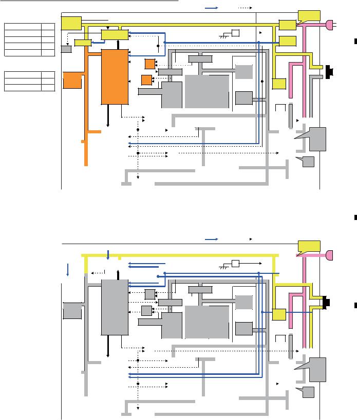
|
5 |
|
6 |
|
7 |
|
8 |
|
Power supply status - Active standby (Main switch off)
A
ON |
OFF |
Microcomputer |
|
|
|
|
|
|
|
|
Power supply |
V+3.3V_STB |
AC |
output port state |
|
IR/Key/ |
|
|
|
|
|
|
V+5.1V_STB |
||
|
|
|
|
|
|
|
STB |
|
|
||
IF: ACTIVE |
ON |
232C |
|
AC_DET |
|
|
|
|
|
|
|
Main: RELAY2 |
OFF |
|
IF ucom |
|
|
|
R |
|
|
|
|
|
|
|
|
|
|
|
|
||||
Main: PSW1 |
OFF |
|
|
M_SW_DET |
|
|
|
US_SW |
AC_ |
|
|
SW |
|
|
|
|
|
|
|
||||
Module: RELAY |
OFF |
ACTIVE |
M_SW_DET_B |
|
|
|
|
DET |
|
|
|
LED |
|
|
|
|
|
|
|
||||
Module: DRF_B |
OFF |
|
|
|
|
|
|
|
|
||
|
|
|
|
|
|
|
|
|
Main |
||
|
|
|
|
RST3 |
|
DCDC/REG |
|
I/O |
|
|
|
Microcomputer |
|
|
|
|
|
|
|
Switch |
|||
|
|
|
RST4 AND |
PDET |
|
|
|
|
|||
input port state |
|
|
|
|
|
|
|
|
|
|
|
|
|
|
|
DCDC/REG |
|
|
MSPAP |
|
|
|
|
Main: RST4 |
OFF |
EEPROM |
Main_ |
PSW1 |
|
|
|
|
|
||
|
|
|
|
|
|
|
|||||
Main: RST2 |
OFF |
VBI/ |
ucom |
AND |
|
AA.D.TUNER. |
AV-SW |
|
M_SW |
|
|
Module: RST2 |
OFF |
USB |
|
RST2 |
VDEC |
AD.TUNER |
FAN |
|
_DET |
|
B |
|
|
EMG_USB |
VBI |
|
|
|
|
|
|||
|
|
|
|
HDMI |
D.TUNERBCM |
RGB-SW |
|
|
|
|
|
|
|
|
|
|
ASIC |
D-AMP |
|
|
|
||
|
|
|
|
|
iLink(XDA)POD |
Jumper |
|
|
|||
|
|
|
|
|
LVDS-Tx |
USB(RegAAC-DEC.) |
AD |
|
|
|
|
|
Main |
|
|
|
|
|
|
RELAY2 |
|
|
|
|
|
|
|
|
|
|
|
|
|
|
|
|
|
|
|
P11 |
|
|
|
|
|
|
|
|
|||||||||||||
|
|
|
|
|
|
|
|
|
|
|
|
|
|
|
|
|
|
|
|
|
|
|
|
|
|
|
|
|
|
|
|||||||||||||||||||
|
|
|
|
|
|
|
|
|
|
|
|
|
|
|
|
|
|
|
|
|
|
|
|
|
|
|
|
|
|
|
|
|
|
|
|
|
|
|
|
|
|
|
|
|
|
|
|
|
|
|
|
|
|
|
|
|
|
|
|
|
|
|
|
|
|
|
OR |
|
|
|
|
|
|
|
|
|
|
|
|
|
|
|
|
|
|
|
|
|
|
|
|
|
|
|
|
|
|
|
|
|
|
|
|
|
|
|
|
|
|
|
|
|
|
|
|
|
|
|
|
|
|
|
|
|
|
|
|
|
|
|
|
|
|
|
|
|
|
|
|
|
|
|
Relay |
|
|
|
|||
|
|
|
|
|
|
|
|
|
|
|
|
|
|
|
|
|
|
|
|
|
|
|
|
|
|
|
|
|
|
LVDS-Rx |
|
|
|
|
|
|
|
|
|
|
|
|
|
|
|
|
|
|
|
|
|
|
|
|
|
|
|
|
|
|
|
|
|
|
|
RELAY |
|
|
|
|
|
|
|
|
|
|
|
|
|
|
|
|
|
|
|
|
|
|
|
|
|
|
|
||||||
|
|
|
|
|
|
|
|
|
|
|
|
|
|
|
|
|
|
|
|
|
DCDC/REG |
|
|
|
|
DAC |
|
|
|
|
|
|
|
Vcc |
|
|
|
|
V+35V |
|
|||||||||
|
|
|
|
|
|
|
|
|
|
|
|
|
|
|
|
|
|
|
|
|
|
|
|
|
|
|
|
|
|
SQ ASIC |
|
|
|
|
|
|
|
|
|
|
|
V+16.5V |
|||||||
|
|
|
|
|
|
|
|
|
Module_ |
|
|
|
|
|
|
|
|
|
|
|
|
RST2 |
|
|
|
|
|
|
|
|
|
|
|
|
|
|
|
|
V+12V |
||||||||||
|
EEPROM |
|
|
|
|
|
|
|
|
ucom |
|
|
|
|
|
|
|
|
|
|
|
|
|
|
|
|
|
|
|
|
|
|
|
|
|
|
|
|
|
|
|
|
|
V+6.5V |
|||||
|
|
|
|
|
|
|
|
|
|
|
|
|
|
|
|
|
|
|
|
|
|
|
|
|
|
|
|
|
|
|
|
|
|
|
|
|
|
|
|
|
|||||||||
|
|
|
|
|
|
|
|
|
|
|
|
|
|
|
|
|
|
|
|
|
|
|
|
|
|
|
|
|
|
|
|
|
|
|
|
|
|
|
Vsus |
|
|
|
|
V+5.1V |
|||||
|
|
|
|
|
|
|
|
|
|
|
|
|
|
|
|
|
|
|
|
AND |
|
|
|
|
|
|
|
|
|
|
|
|
|
|
|
|
|
|
|
|
|
|
|
|
|||||
|
Digital |
|
|
|
|
|
|
|
|
|
|
|
|
|
DRF_B |
|
|
|
|
|
|
|
|
|
|
|
|
|
|
|
|
Vadr |
|
|
|
VSUS |
|||||||||||||
|
|
|
|
|
|
|
|
|
|
|
|
|
|
|
|
|
|
|
|
|
|
|
|
|
|
|
|
|
|
|
|
|
|
|
|
|
|
|
|||||||||||
|
|
|
|
|
|
|
|
|
|
|
|
|
|
|
|
|
|
|
|
|
|
|
|
|
|
|
|
|
|
|
|
|
|
|
|
|
|
|
|
|
|
|
|
|
VADR |
||||
|
|
|
|
|
|
|
|
X/Y Drive |
|
|
|
|
|
|
|
Address |
|
|
|
|
|
|
|
|
|
|
|
|
|
|
|
|
|||||||||||||||||
|
|
BAK_EEP |
|
|
|
|
|
|
|
|
|
ASIC |
|
ADDRESS |
|
|
|
|
|
|
|
|
|
|
|
|
|
|
|
|
|
|
|||||||||||||||||
|
|
|
|
Scan |
|
|
|
|
|
|
|
|
|
|
|
|
|
|
|
|
|
|
|
|
|
|
|
|
|
|
|
|
|
|
C |
||||||||||||||
|
|
|
|
|
|
|
|
|
|
|
|
|
|
|
|
|
|
|
|
|
|
|
|
|
|
|
|
|
|
|
|
|
|
|
|
|
|
|
|
|
|
|
|
|
|
|
|
||
|
|
|
|
|
|
|
|
|
DRIVE |
|
|
|
|
|
|
|
|
|
|
|
|
|
|
|
|
|
|
|
|
|
|
|
|
|
|
|
|
|
|
|
|
|
|
|
|
|
|
||
|
Sensor |
|
|
|
|
|
|
DCDC/REG |
|
|
|
|
|
|
|
|
|
|
|
|
|
|
|
|
|
|
|
|
|
DRIVE/SCAN |
|
|
|
||||||||||||||||
|
|
|
|
|
|
|
|
|
|
|
|
|
|
|
|
|
|
|
|
|
|
|
|
|
|
|
|
|
|
|
|
||||||||||||||||||
|
|
|
|
|
|
|
|
|
|
|
|
|
|
|
|
|
|
|
|
|
|
|
|
|
|
|
|
|
|
|
|
|
|
|
|
|
|
|
|
|
|
|
|
||||||
|
|
|
|
|
|
|
|
|
|
|
|
|
|
|
|
|
|
|
|
|
|
|
|
|
|
|
|
|
|
|
|
|
|
|
|
|
|
|
|
|
|
|
|
|
|
|
|
|
|
The user operation is invalid. (All LED: OFF)
Standby power devices (periphery of IF/Main/Module microcomputer) operate.
Power supply status - Passive standby
Microcomputer output port state
IF: ACTIVE |
OFF |
|
Main: RELAY2 |
OFF |
|
Main: PSW1 |
OFF |
|
Module: RELAY |
OFF |
|
Module: DRF_B |
OFF |
|
Microcomputer |
|
|
input port state |
|
|
Main: RST4 |
OFF |
|
Main: RST2 |
OFF |
|
Module: RST2 |
OFF |
|
|
|
|
|
|
|
|
|
|
|
|
|
|
|
|
|
|
ON |
OFF |
|
|
|
|
|
|
|
|
|
|
|
|
|
|
|
|
|
|
|
|
|
|
|
|
|
|
|
|
|
|
|
|
|
|
|
|
Power supply |
V+3.3V_STB |
|
AC |
|||||||||
|
|
|
|
|
|
|
|
|
|
|
|
|
|
|
|
|
|
|
|
|
|
||||||||||||
IR/Key/ |
|
|
|
|
|
|
|
|
|
|
|
|
|
|
|
|
|
V+5.1V_STB |
|
||||||||||||||
|
|
|
|
|
|
|
|
|
|
|
|
|
|
|
|
|
|
|
|
|
STB |
|
|
|
|
|
|
|
|
||||
232C |
|
|
|
|
|
|
|
|
|
|
|
|
|
|
|
|
|
|
|
|
|
|
|
|
|
|
|
|
|
||||
|
|
|
|
|
|
|
|
IF ucom |
AC_DET |
|
R |
US_SW |
|
|
|
|
|
|
|
|
|
|
|
|
D |
||||||||
|
|
|
|
|
|
|
|
|
|
|
|
|
|
|
|
|
|
|
|
|
|
|
|
|
|||||||||
|
|
|
|
|
|
|
|
|
|
|
|
|
|
M_SW_DET |
|
|
|
|
|
|
|
|
|
AC_ |
|
|
|
|
|
|
|
|
|
|
|
|
SW |
|
ACTIVE |
"kill me" |
|
|
|
|
|
|
|
|
|
|
DET |
|
|
|
|
|
|
|
|
||||||||
|
|
|
|
|
|
|
|
|
|
|
|
|
|
|
|
|
|
|
|
|
|||||||||||||
|
|
|
|
|
|
|
|
|
|
|
|
|
|
|
|
|
|
|
|||||||||||||||
LED |
|
|
|
|
|
|
|
|
|
|
|
|
M_SW_DET_B |
|
|
|
|
|
|
|
|
|
|
|
|
|
|
|
|
|
|
|
|
|
|
|
|
|
|
|
|
|
|
|
|
|
|
|
|
|
|
|
|
|
|
|
|
|
|
|
|
|
|||||
|
|
RST3 |
|
|
DCDC/REG |
|
I/O |
Main |
|
|
AND |
PDET |
|
Switch |
|||
|
|
RST4 |
|
|
||||
|
|
|
|
|
|
|
||
EEPROM |
Main_ |
PSW1 |
|
DCDC/REG |
|
|
MSPAP |
|
|
|
|
|
|
|
|||
VBI/ |
ucom |
|
AND |
|
AA.D.TUNER. |
AV-SW |
|
M_SW |
USB |
|
RST2 |
|
VDEC |
DA.TUNER |
FAN |
|
_DET |
|
EMG_USB |
VBI |
|
|||||
|
|
|
HDMI |
|
|
|
||
|
|
|
D.TUNERBCM |
RGB-SW |
|
|
||
|
|
|
|
ASIC |
D-AMP |
|
||
|
|
|
|
iLink(XDA)POD |
Jumper |
|||
|
|
|
|
LVDS-Tx |
USB(RegAAC-DEC.) |
AD |
|
|
|
|
|
|
|
|
|
|
|
Main |
|
|
|
|
|
|
RELAY2 |
|
|
|
|
|
|
|
|
|
|
|
|
|
P11 |
|
|
|
|
|
|
|
|
E |
||||||||||||||||||
|
|
|
|
|
|
|
|
|
|
|
|
|
|
|
|
|
|
|
|
|
|
|
|
|
|||||||||||||||||||||||||
|
|
|
|
|
|
|
|
|
|
|
|
|
|
|
|
|
|
|
|
|
|
|
|
|
|
|
|
|
|
|
|
|
|
|
|
|
|
|
|
|
|
|
|
|
|
||||
|
|
|
|
|
|
|
|
|
|
|
|
|
|
|
|
OR |
|
|
|
|
|
|
|
|
|
|
|
|
|
|
|
|
|
|
|
|
|
|
|
|
|
|
|
|
|
|
|||
|
|
|
|
|
|
|
|
|
|
|
|
|
|
|
|
|
|
|
|
|
|
|
|
|
|
|
|
|
|
|
|
|
|
|
|
|
|
|
|
|
|
Relay |
|
|
|||||
|
|
|
|
|
|
|
|
|
|
|
|
|
|
|
RELAY |
|
|
|
|
|
|
|
|
|
|
|
|
LVDS-Rx |
|
|
|
|
|
|
|
|
|
|
|
|
|
|
|
|
|
|
|||
|
|
|
|
|
|
|
|
|
|
|
|
|
|
|
|
|
|
|
|
DCDC/REG |
|
|
|
|
DAC |
|
|
|
|
|
|
Vcc |
|
|
|
|
|
V+35V |
|
||||||||||
|
|
|
|
|
|
|
|
|
|
|
|
|
|
|
|
|
|
|
|
|
|
|
|
|
|
|
|
|
SQ ASIC |
|
|
|
|
|
|
|
|
|
|
|
|
V+16.5V |
|
||||||
|
|
|
|
|
|
|
|
|
Module_ |
|
|
|
|
|
|
|
|
|
|
|
RST2 |
|
|
|
|
|
|
|
|
|
|
|
|
|
|
|
|
|
V+12V |
|
|||||||||
|
EEPROM |
|
|
|
|
|
|
|
|
ucom |
|
|
|
|
|
|
|
|
|
|
|
|
|
|
|
|
|
|
|
|
|
|
|
|
|
|
|
|
|
|
|
|
|
V+6.5V |
|
||||
|
|
|
|
|
|
|
|
|
|
|
|
|
|
|
|
|
|
|
|
|
|
|
|
|
|
|
|
|
|
|
|
|
|
|
|
|
|
|
|
|
|
||||||||
|
|
|
|
|
|
|
|
|
|
|
|
|
|
|
|
|
|
|
|
|
|
|
|
|
|
|
|
|
|
|
|
|
|
|
|
|
|
Vsus |
|
|
|
|
|
V+5.1V |
|
||||
|
|
|
|
|
|
|
|
|
|
|
|
|
|
|
|
|
|
|
AND |
|
|
|
|
|
|
|
|
|
|
|
|
|
|
|
|
|
|
|
|
|
|
|
|
|
|||||
|
Digital |
|
|
|
|
|
|
|
|
|
|
|
|
DRF_B |
|
|
|
|
|
|
|
|
|
|
|
|
|
|
|
|
Vadr |
|
|
|
VSUS |
|
|||||||||||||
|
|
|
|
|
|
|
|
|
|
|
|
|
|
|
|
|
|
|
|
|
|
|
|
|
|
|
|
|
|
|
|
|
|
|
|
|
|||||||||||||
|
|
|
|
|
|
|
|
|
|
|
|
|
|
|
|
|
|
|
|
|
|
|
|
|
|
|
|
|
|
|
|
|
|
|
|
|
|
|
|
|
|
|
|
VADR |
|
||||
|
|
BAK_EEP |
|
X/Y Drive |
|
|
|
|
|
|
Address |
ASIC |
|
ADDRESS |
|
|
|
|
|
|
|
|
|
|
|
|
|
|
|
|
|
|
|
||||||||||||||||
|
|
|
Scan |
|
|
|
|
|
|
|
|
|
|
|
|
|
|
|
|
|
|
|
|
|
|
|
|
|
|
|
|
|
|
|
|
||||||||||||||
|
|
|
|
|
|
|
|
|
|
|
|
|
|
|
|
|
|
|
|
|
|
|
|
|
|
|
|
|
|
|
|
|
|
|
|
|
|
|
|||||||||||
|
|
|
|
|
|
|
|
|
DRIVE |
|
|
|
|
|
|
|
|
|
|
|
|
|
|
|
|
|
|
|
|
|
|
|
|
|
|
|
|
|
|
|
|
|
|
|
|
|
|
||
|
Sensor |
|
|
|
|
DCDC/REG |
|
|
|
|
|
|
|
|
|
|
|
|
|
|
|
|
|
|
|
|
|
DRIVE/SCAN |
|
|
|
||||||||||||||||||
|
|
|
|
|
|
|
|
|
|
|
|
|
|
|
|
|
|
|
|
|
|
|
|
|
|
|
|
|
|
|
|
|
|
|
|
|
|
|
|
|
|
|
|
||||||
Remote control unit waiting state. (Red LED: ON)
Among standby power devices, only the IF microcomputer periphery operates.
F
|
23 |
|
PDP-508XG |
||
|
|
5 |
|
6 |
|
7 |
|
8 |
|
|
|
|
|
|
||||
|
|
|
|
|

|
1 |
|
2 |
|
3 |
|
4 |
|
A
Power supply status - Active standby
Microcomputer output port state
|
|
IF: ACTIVE |
ON |
|
|
Main: RELAY2 |
OFF |
|
|
Main: PSW1 |
OFF |
|
|||
|
|
Module: RELAY |
OFF |
|
|
Module: DRF_B |
OFF |
|
|
Microcomputer |
|
|
|
input port state |
|
|
|
Main: RST4 |
OFF |
B |
|
Main: RST2 |
OFF |
|
|
Module: RST2 |
OFF |
|
|
|
|
|
|
|
|
C
ON |
OFF |
Power supply |
V+3.3V_STB |
AC |
V+5.1V_STB |
IR/Key/
232C 


 STB
STB
|
|
|
|
|
|
|
|
|
AC_DET |
|
|
|
|
|
|
|
|
||
|
|
|
|
|
|
|
|
IF ucom |
|
R |
US_SW |
|
|
|
|
|
|||
|
|
|
|
|
|
|
|
|
|
|
|
|
|
|
|
|
|||
|
|
|
|
|
|
|
|
|
M_SW_DET |
|
|
|
|
|
|
|
AC_ |
|
|
|
|
|
SW |
|
|
|
|
|
|
|
|
|
|
|
|
|
DET |
|
|
|
|
|
ACTIVE |
|
|
|
|
|
|
|
|
|
|||||||
LED |
|
|
|
|
|
|
|
M_SW_DET_B |
|
|
|
|
|
|
|
|
|
|
|
|
|
|
|
|
|
|
|
|
|
|
|
|
|
|
|||||
|
|
RST3 |
|
|
DCDC/REG |
|
I/O |
Main |
|
|
AND |
PDET |
|
Switch |
|||
|
|
RST4 |
|
|
|
|||
|
|
|
|
|
|
|
||
|
|
|
|
|
|
|
|
|
EEPROM |
Main_ |
PSW1 |
|
DCDC/REG |
|
|
MSPAP |
|
|
|
|
|
|
|
|||
VBI/ |
ucom |
|
AND |
|
AA.D.TUNER. |
AV-SW |
|
M_SW |
USB |
|
RST2 |
|
VDEC |
AD..TUNER |
FAN |
|
_DET |
|
|
VBI |
|
|||||
|
|
EMG_USB |
HDMI |
|
|
|
||
|
|
D.TUNERBCM |
RGB-SW |
|
|
|||
|
|
|
|
ASIC |
iLink(XDA)POD |
D-AMP |
Jumper |
|
|
|
|
|
LVDS-Tx |
USB(RegAAC-DEC.) |
AD |
|
|
|
Main |
|
|
|
|
|
|
RELAY2 |
|
|
|
|
|
|
|
|
|
|
|
|
P11 |
|
|
|
|
|
|
|
|
||||||||||||||||||||
|
|
|
|
|
|
|
|
|
|
|
|
|
|
|
|
|
|
|
|
|
|
|
|
||||||||||||||||||||||||||
|
|
|
|
|
|
|
|
|
|
|
"POF" |
|
|
|
|
|
|
|
|
|
|
|
|
|
|
|
|
|
|
|
|
|
|
|
|
|
|
|
|
|
|
|
|
|
|
|
|
|
|
|
|
|
|
|
|
|
|
|
|
|
|
|
|
|
OR |
|
|
|
|
|
|
|
|
|
|
|
|
|
|
|
|
|
|
|
|
|
|
|
|
|
|
|
|
|
|
|
|
||
|
|
|
|
|
|
|
|
|
|
|
|
|
|
|
|
|
|
|
|
|
|
|
|
|
|
|
|
|
|
|
|
|
|
|
|
|
|
|
|
|
Relay |
|
|
||||||
|
|
|
|
|
|
|
|
|
|
|
|
|
|
|
|
|
|
|
|
|
|
|
|
|
|
|
|
|
|
|
|
|
|
|
|
|
|
|
|
|
|
|
|
|
|||||
|
|
|
|
|
|
|
|
|
|
|
|
|
|
|
|
|
|
|
|
|
|
|
|
|
|
|
|
|
|
|
|
|
|
|
|
|
|
|
|
|
|
|
|
|
|
|
|
|
|
|
|
|
|
|
|
|
|
|
|
|
|
|
|
|
|
RELAY |
|
|
|
|
|
|
|
|
|
|
|
|
LVDS-Rx |
|
|
|
|
|
|
|
|
|
|
|
|
|
|
|
|
|
|||
|
|
|
|
|
|
|
|
|
|
|
|
|
|
|
|
|
|
|
|
|
DCDC/REG |
|
|
|
|
DAC |
|
|
|
|
|
|
Vcc |
|
|
|
|
|
V+35V |
||||||||||
|
|
|
|
|
|
|
|
|
|
|
|
|
|
|
|
|
|
|
|
|
|
|
|
|
|
|
|
|
|
SQ ASIC |
|
|
|
|
|
|
|
|
|
|
|
|
V+16.5V |
||||||
|
|
|
|
|
|
|
|
|
Module_ |
|
|
|
|
|
|
|
|
|
|
|
|
RST2 |
|
|
|
|
|
|
|
|
|
|
|
|
|
|
|
|
|
V+12V |
|||||||||
|
EEPROM |
|
|
|
|
|
|
|
|
ucom |
|
|
|
|
|
|
|
|
|
|
|
|
|
|
|
|
|
|
|
|
|
|
|
|
|
|
|
|
|
|
|
|
|
|
V+6.5V |
||||
|
|
|
|
|
|
|
|
|
|
|
|
|
|
|
|
|
|
|
|
|
|
|
|
|
|
|
|
|
|
|
|
|
|
|
|
|
|
|
|
|
|
||||||||
|
|
|
|
|
|
|
|
|
|
|
|
|
|
|
|
|
|
|
|
|
|
|
|
|
|
|
|
|
|
|
|
|
|
|
|
|
|
|
Vsus |
|
|
|
|
|
V+5.1V |
||||
|
|
|
|
|
|
|
|
|
|
|
|
|
|
|
|
|
|
|
|
AND |
|
|
|
|
|
|
|
|
|
|
|
|
|
|
|
|
|
|
|
|
|
|
|
|
|||||
Digital |
|
|
|
|
|
|
|
|
|
|
|
|
|
DRF_B |
|
|
|
|
|
|
|
|
|
|
|
|
|
|
|
Vadr |
|
|
|
VSUS |
|||||||||||||||
|
|
|
|
|
|
|
|
|
|
|
|
|
|
|
|
|
|
|
|
|
|
|
|
|
|
|
|
|
|
|
|
|
|
|
|
|
|
|
|
|
|
|
|
|
VADR |
||||
|
|
|
|
|
|
|
X/Y Drive |
|
|
|
|
|
|
|
Address |
|
|
|
|
|
|
|
|
|
|
|
|
|
|
|
|
||||||||||||||||||
|
|
BAK_EEP |
|
|
|
|
|
|
|
|
ASIC |
|
ADDRESS |
|
|
|
|
|
|
|
|
|
|
|
|
|
Power |
||||||||||||||||||||||
|
|
|
|
|
|
|
|
Scan |
|
|
|
|
|
|
|
|
|
|
|
|
|
|
|
|
|
|
|
|
|
|
|
|
|
|
|
||||||||||||||
|
|
|
|
|
|
|
|
|
DRIVE |
|
|
|
|
|
|
|
|
|
|
|
|
|
|
|
|
|
|
|
|
|
|
|
|
|
|
|
|
|
|
|
|
|
|
|
|
|
|
||
Sensor |
|
|
|
DCDC/REG |
|
|
|
|
|
|
|
|
|
|
|
|
|
|
|
|
|
|
|
|
|
DRIVE/SCAN |
|
|
|||||||||||||||||||||
|
|
|
|
|
|
|
|
|
|
|
|
|
|
|
|
|
|
|
|
|
|
|
|
|
|
||||||||||||||||||||||||
|
|
|
|
|
|
|
|
|
|
|
|
|
|
|
|
|
|
|
|
|
|
|
|
|
|
|
|
|
|
|
|
|
|
|
|
|
|
|
|
|
|
|
|||||||
|
|
|
|
|
|
|
|
|
|
|
|
|
|
|
|
|
|
|
|
|
|
|
|
|
|
|
|
|
|
|
|
|
|
|
|
|
|
|
|
|
|
|
|
|
|
|
|
|
|
Remote control unit waiting state. (Red LED: ON)
Standby power devices (periphery of IF/Main/Module microcomputer) operate.
|
Power supply status - Functional standby |
|
|
|
|
|
|
|
||||
|
|
|
|
|
|
|
ON |
|
OFF |
|
V+3.3V_STB |
|
|
Microcomputer |
|
|
|
|
|
|
|
|
Power supply |
AC |
|
|
|
|
|
|
|
|
|
|
V+5.1V_STB |
|||
|
output port state |
|
IR/Key/ |
|
|
|
|
|
|
|||
D |
|
|
|
|
|
|
|
|
|
|||
|
|
|
|
|
|
|
STB |
|
|
|||
|
IF: ACTIVE |
ON |
232C |
|
AC_DET |
|
|
|
|
|
|
|
|
|
|
|
|
|
R |
|
|
|
|||
|
Main: RELAY2 |
ON |
|
IF ucom |
|
|
|
|
|
|
||
|
|
|
|
|
|
|
|
|
||||
|
Main: PSW1 |
OFF |
|
|
M_SW_DET |
|
|
|
US_SW |
AC_ |
|
|
|
SW |
|
|
|
|
|
|
|
||||
|
Module: RELAY |
OFF |
ACTIVE |
M_SW_DET_B |
|
|
|
|
DET |
|
|
|
|
LED |
|
|
|
|
|
|
|
||||
|
Module: DRF_B |
OFF |
|
|
|
|
|
|
|
|
||
|
|
|
RST3 |
|
|
|
|
|
Main |
|||
|
|
|
|
|
PDET DCDC/REG |
|
I/O |
|
||||
|
Microcomputer |
|
|
|
|
|
Switch |
|||||
|
|
|
|
RST4 AND |
|
|
||||||
|
input port state |
|
|
|
|
|
|
MSPMAP |
|
|
|
|
|
Main: RST4 |
ON |
EEPROM |
Main_ |
DCDC/REG |
|
|
|
|
|
||
|
PSW1 |
|
|
|
|
|
|
|
||||
|
Main: RST2 |
OFF |
VBI/ |
ucom |
AND |
|
AA.D.TUNER. |
AV-SW |
|
M_SW |
|
|
|
Module: RST2 |
OFF |
USB |
|
RST2 |
VDEC |
AD..TUNER |
FAN |
|
_DET |
|
|
|
|
VBI |
|
|
|
|||||||
|
|
|
|
|
EMG_USB |
HDMI |
|
|
|
|
|
|
|
|
|
|
|
D.TUNERBCM |
|
|
|
|
|
||
|
|
|
|
|
|
ASIC |
RGB-SW |
D-AMP |
|
|
|
|
|
|
|
|
|
|
iLink(XDA)POD |
Jumper |
|
|
|||
|
|
|
|
|
|
LVDS-Tx |
USB(RegAAC-DEC.) |
AD |
|
|
|
|
E |
|
|
Main |
|
|
|
|
|
|
RELAY2 |
|
|
|
|
|
|
|
|
|
|
|
|
|
|
|
|
|
|
|
|
P11 |
|
|
|
|
|
|
|
|||||||||||||
|
|
|
|
|
|
|
|
|
|
|
|
|
|
|
|
|
|
|
|
|
|
|
|
|
|
|
|
|
|
|
|
|
|
||||||||||||||||||
|
|
|
|
|
|
|
|
|
|
|
|
|
"POF" |
|
|
|
|
|
|
|
|
|
|
|
|
|
|
|
|
|
|
|
|
|
|
|
|
|
|
|
|
|
|
|
|
|
|
|
|
|
|
|
|
|
|
|
|
|
|
|
|
|
|
|
|
|
|
|
OR |
|
|
|
|
|
|
|
|
|
|
|
|
|
|
|
|
|
|
|
|
|
|
|
|
|
|
|
|
|
|
|
|
||
|
|
|
|
|
|
|
|
|
|
|
|
|
|
|
|
|
|
|
|
|
|
|
|
|
|
|
|
|
|
|
|
|
|
|
|
|
|
|
|
|
|
|
|
|
Relay |
|
|||||
|
|
|
|
|
|
|
|
|
|
|
|
|
|
|
|
|
|
|
|
|
|
|
|
|
|
|
|
|
|
|
|
|
|
|
|
|
|
||||||||||||||
|
|
|
|
|
|
|
|
|
|
|
|
|
|
|
|
|
|
|
|
|
|
|
|
|
|
|
|
|
|
|
|
LVDS-Rx |
|
|
|
|
|
|
|
|
|
|
|
|
|
|
|
|
|
||
|
|
|
|
|
|
|
|
|
|
|
|
|
|
|
|
|
|
RELAY |
DCDC/REG |
|
|
|
|
|
|
|
|
|
|
|
|
|
|
|
|
|
|
V+35V |
|||||||||||||
|
|
|
|
|
|
|
|
|
|
|
|
|
|
|
|
|
|
|
|
|
|
|
|
|
|
DAC |
|
|
|
|
|
|
|
Vcc |
|
|
|
|
|||||||||||||
|
|
|
|
|
|
|
|
|
|
|
|
|
|
|
|
|
|
|
|
|
|
|
|
|
|
|
|
|
|
|
|
SQ ASIC |
|
|
|
|
|
|
|
|
|
|
|
|
V+16.5V |
||||||
|
|
|
|
|
|
|
|
|
|
|
Module_ |
|
|
|
|
|
|
|
|
|
|
|
|
RST2 |
|
|
|
|
|
|
|
|
|
|
|
|
|
|
|
|
|
V+12V |
|||||||||
|
|
|
EEPROM |
|
|
|
|
|
|
|
|
|
|
|
|
|
|
|
|
|
|
|
|
|
|
|
|
|
|
|
|
|
|
|
|
|
|
|
|
|
|
V+6.5V |
|||||||||
|
|
|
|
|
|
|
|
|
|
|
|
|
ucom |
|
|
|
|
|
|
|
|
|
|
|
|
|
|
|
|
|
|
|
|
|
|
|
|
|
|
|
Vsus |
|
|
|
|
V+5.1V |
|||||
|
|
|
|
|
|
|
|
|
|
|
|
|
|
|
|
|
|
|
|
|
|
|
|
|
|
|
|
|
|
|
|
|
|
|
|
|
|
|
|
|
|
|
|
|
|
||||||
|
|
|
|
|
|
|
|
|
|
|
|
|
|
|
|
|
|
|
|
|
|
AND |
|
|
|
|
|
|
|
|
|
|
|
|
|
|
|
|
|
|
|
|
|
|
|
|
|||||
|
|
|
Digital |
|
|
|
|
|
|
|
|
|
|
|
|
|
DRF_B |
|
|
|
|
|
|
|
|
|
|
|
|
|
|
|
|
|
Vadr |
|
|
|
VSUS |
||||||||||||
|
|
|
|
|
|
|
|
|
|
|
|
|
|
|
|
|
|
|
|
|
|
|
|
|
|
|
|
|
|
|
|
|
|
|
|
|
|
|
|
|
|
|
|
|
|
|
|
VADR |
|||
|
|
|
|
|
|
|
|
|
X/Y Drive |
|
|
|
|
|
|
|
Address |
|
|
|
|
|
|
|
|
|
|
|
|
|
|
|
|
|
|||||||||||||||||
|
|
|
|
BAK_EEP |
|
|
|
|
|
|
|
|
ASIC |
|
ADDRESS |
|
|
|
|
|
|
|
|
|
|
|
|
|
|
|
|
|
|
||||||||||||||||||
|
|
|
|
|
Scan |
|
|
|
|
|
|
|
|
|
|
|
|
|
|
|
|
|
|
|
|
|
|
|
|
|
|
|
|
|
|
|
|
||||||||||||||
|
|
|
|
|
|
|
|
|
|
|
DRIVE |
|
|
|
|
|
|
|
|
|
|
|
|
|
|
|
|
|
|
|
|
|
|
|
|
|
|
|
|
|
|
|
|
|
|
|
|
|
|
||
|
|
|
Sensor |
|
|
|
|
|
|
DCDC/REG |
|
|
|
|
|
|
|
|
|
|
|
|
|
|
|
|
|
|
|
|
|
|
|
|
DRIVE/SCAN |
|
|||||||||||||||
|
|
|
|
|
|
|
|
|
|
|
|
|
|
|
|
|
|
|
|
|
|
|
|
|
|
|
|
|
|
||||||||||||||||||||||
|
|
|
|
|
|
|
|
|
|
|
|
|
|
|
|
|
|
|
|
|
|
|
|
|
|
|
|
|
|
|
|
|
|
|
|
|
|
|
|
|
|
|
|
|
|
||||||
|
|
|
|
|
|
|
|
|
|
|
|
|
|
|
|
|
|
|
|
|
|
|
|
|
|
|
|
|
|
|
|
|
|
|
|
|
|
|
|
|
|
|
|
|
|
|
|
|
|
|
|
F
24
Remote control unit waiting state. (Red LED: ON)
Standby power device and some Vcc power devices operate.
RGB-SW/AD/D-AMP are electrified, but uses the power-saving mode function of the IC.
PDP-508XG
1 |
|
2 |
|
3 |
|
4 |
|

|
5 |
|
6 |
|
7 |
|
8 |
|
Power supply status - ON |
|
|
|
|
|
|
|
|
|
A |
||
|
|
|
|
|
|
ON |
|
OFF |
|
|
V+3.3V_STB |
|
Microcomputer |
|
|
|
|
|
|
|
|
|
Power supply |
AC |
|
output port state |
|
IR/Key/ |
|
|
|
|
|
|
|
V+5.1V_STB |
||
|
|
|
|
|
|
|
|
STB |
|
|
||
IF: ACTIVE |
ON |
232C |
|
AC_DET |
|
|
|
|
|
|
|
|
|
|
|
|
|
R |
|
|
|
|
|||
Main: RELAY2 |
ON |
|
IF ucom |
|
|
|
|
|
|
|
||
|
M_SW_DET |
|
|
|
US_SW |
AC_ |
|
|
||||
Main: PSW1 |
ON |
|
|
|
|
|
|
|
|
|||
SW |
|
|
|
|
|
|
|
|
||||
Module: RELAY |
ON |
ACTIVE |
M_SW_DET_B |
|
|
|
|
|
DET |
|
|
|
LED |
|
|
|
|
|
|
|
|
||||
Module: DRF_B |
ON |
|
|
|
|
|
|
|
|
|
||
|
|
RST3 |
|
|
|
|
|
|
Main |
|||
|
|
|
|
|
DCDC/REG |
I/O |
|
|||||
Microcomputer |
|
|
|
PDET |
|
Switch |
||||||
|
|
|
RST4 AND |
|
||||||||
input port state |
|
|
|
DCDC/REG |
|
|
|
MSP |
|
|
|
|
Main: RST4 |
ON |
EEPROM |
Main_ |
PSW1 |
|
|
|
|
|
|
||
|
|
|
|
|
|
|
|
|||||
Main: RST2 |
ON |
VBI/ |
ucom |
AND |
|
A.TUNER |
AV-SW |
|
|
M_SW |
|
B |
Module: RST2 |
ON |
USB |
|
RST2 |
VDEC |
FAN |
|
|
_DET |
|
||
|
|
|
|
EMG_USB |
HDMI |
D.TUNER |
RGB-SW |
|
|
|
|
|
|
|
|
|
|
ASIC |
|
D-AMP |
|
|
|
||
|
|
|
|
|
(XDA) |
|
Jumper |
|
|
|||
|
|
Main |
|
RELAY2 |
LVDS-Tx |
|
AD |
|
|
|
|
|
|
|
|
|
|
|
|
|
P11 |
|
|
||
|
|
|
"PON" |
OR |
|
|
|
|
|
|
Relay |
|
|
|
|
|
|
|
|
|
|
|
|
||
|
|
|
|
|
|
|
|
|
|
|
|
|
|
|
|
|
|
|
|
|
|
|
|
|
|
|
RELAY |
|
|
|
|
|
|
|
LVDS-Rx |
|
|
|
|
|
|
|
|
|
|
V+35V |
|
|||||
|
|
|
|
|
|
|
|
|
|
|
|
|
|
|
|
DCDC/REG |
|
|
|
|
|
DAC |
|
|
|
|
Vcc |
|
|
|
|
||||||||
|
|
|
|
|
|
|
|
|
|
|
|
|
|
|
|
|
|
|
|
|
|
|
SQ ASIC |
|
|
|
|
|
|
|
V+16.5V |
||||||||
|
|
|
|
|
|
|
|
|
Module_ |
|
|
|
|
|
|
RST2 |
|
|
|
|
|
|
|
|
|
|
|
|
|
V+12V |
|||||||||
|
EEPROM |
|
|
|
|
|
|
|
|
|
|
|
|
|
|
|
|
|
|
|
|
|
|
|
|
|
|
|
|
V+6.5V |
|||||||||
|
|
|
|
|
|
|
|
|
ucom |
|
|
|
|
|
|
|
|
|
|
|
|
|
|
|
|
|
|
|
Vsus |
|
|
|
V+5.1V |
||||||
|
|
|
|
|
|
|
|
|
|
|
|
|
|
|
|
|
|
|
|
|
|
|
|
|
|
|
|
|
|
|
|
|
|||||||
|
|
|
|
|
|
|
|
|
|
|
|
|
|
|
|
AND |
|
|
|
|
|
|
|
|
|
|
|
|
|
|
|
|
|
|
|
|
|||
Digital |
|
|
|
|
|
|
|
|
|
|
DRF_B |
|
|
|
|
|
|
|
|
|
|
|
|
|
Vadr |
|
|
VSUS |
|||||||||||
|
|
|
|
|
|
|
|
|
|
|
|
|
|
|
|
|
|
|
|
|
|
|
|
|
|
|
|
|
|
|
|
|
|
|
VADR |
||||
|
|
|
|
|
|
|
X/Y Drive |
|
|
|
|
|
Address |
|
|
|
|
|
|
|
|
|
|
|
|
|
|
|
|||||||||||
|
|
BAK_EEP |
|
|
|
|
|
|
|
ASIC |
|
ADDRESS |
|
|
|
|
|
|
|
|
|
|
|
|
|
|
|
|
|||||||||||
|
|
|
Scan |
|
|
|
|
|
|
|
|
|
|
|
|
|
|
|
|
|
|
|
|
|
|
|
C |
||||||||||||
|
|
|
|
|
|
|
|
|
|
|
|
|
|
|
|
|
|
|
|
|
|
|
|
|
|
|
|
|
|
||||||||||
|
|
|
|
|
|
|
|
|
DRIVE |
|
|
|
|
|
|
|
|
|
|
|
|
|
|
|
|
|
|
|
|
|
|
|
|
|
|
|
|||
|
Sensor |
|
|
|
|
|
DCDC/REG |
|
|
|
|
|
|
|
|
|
|
|
|
|
|
|
|
|
DRIVE/SCAN |
|
|||||||||||||
|
|
|
|
|
|
|
|
|
|
|
|
|
|
|
|
|
|
|
|
||||||||||||||||||||
|
|
|
|
|
|
|
|
|
|
|
|
|
|
|
|
|
|
|
|
|
|
|
|
|
|
|
|
|
|
|
|
|
|
||||||
|
|
|
|
|
|
|
|
|
|
|
|
|
|
|
|
|
|
|
|
|
|
|
|
|
|
|
|
|
|
|
|
|
|
|
|
|
|
|
|
A state when it displays a picture on the PDP. (Blue LED: ON)
All devices are electrified.
D
E
F
|
25 |
|
PDP-508XG |
||
|
|
5 |
|
6 |
|
7 |
|
8 |
|
|
|
|
|
|
||||
|
|
|
|
|

|
1 |
|
2 |
|
3 |
|
4 |
|
4.2 DIAGNOSIS FLOWCHART OF FAILURE ANALYSIS
4.2.1 VIDEO SYSTEM
A
Flowchart of Failure Analysis for The Video System
=> MA3
The input signal is not displayed.
|
|
Is the Terrestrial analog signal |
Yes |
|
=> ATV |
|
|||
|
|
not displayed? |
|
|
|
|
|
||
|
|
|
|
|
|
|
|
||
B |
|
|
No |
|
|
|
|
|
|
|
|
|
|
Yes |
|
|
|
||
|
|
Is the composite signal input not |
|
=> COMP / S1 |
|
||||
|
|
displayed? |
|
|
|
|
|
||
|
|
|
|
|
|
|
|
||
|
|
|
No |
|
|
|
|
|
|
|
|
|
|
|
|
|
|
||
|
|
Is the S-video signal input not |
Yes |
|
=> COMP / S1 |
|
|||
|
|
displayed? |
|
|
|
|
|
||
|
|
|
|
|
|
|
|
||
|
|
|
No |
|
|
|
|
|
|
|
|
|
|
Yes |
|
|
|||
|
|
Is the component signal input not |
=> COMP / PC1 |
|
|||||
|
|
displayed? |
|
|
|
|
|
||
|
|
|
|
|
|
|
|
||
|
|
|
No |
|
|
|
|
|
|
|
|
|
|
||||||
C |
|
Is the PC signal input not |
Yes |
=> COMP / PC2 |
|
||||
|
|
displayed? |
|
|
|
|
|
||
|
|
|
|
|
|
|
|
||
|
|
|
No |
|
|
|
|
|
• PDP-428XDA and PDP-508XDA Only |
|
|
|
|
|
|
|
|
|
|
|
|
Is the Terrestrial digital signal |
Yes |
=> DTV |
|
||||
|
|
not displayed? |
|
|
|
|
|
||
|
|
|
|
|
|
|
|
||
|
|
|
|
|
|
|
|
|
|
No |
Is the HDMI signal input not displayed?
No
D
Yes Are the data displayed on the  "HDMI SIGNAL INFO" page of
the Factory menu correct?
Yes
Does the result of SIG mode detection on the Factory menu coincide with the input signal data?
Yes
No
No
No problem with the MAIN Assy. |
Replace the MAIN Assy. |
E
F
After changing the source  equipment, check the "HDMI
SIGNAL INFO" data again.
OK
The source equipment previously used is in failure.
No problem with the MAIN Assy.
Is the sync signal output from
IC5201?
Yes
NG
Replace the MAIN Assy.
No
Replace the MAIN Assy.
No
Is the sync signal input to IC8001?  Replace the MAIN Assy.
Yes
Replace the MAIN Assy.
26 |
|
|
PDP-508XG |
|
|
|
|
|||
|
1 |
|
2 |
|
|
|
3 |
|
4 |
|
|
|
|
|
|
|
|
||||
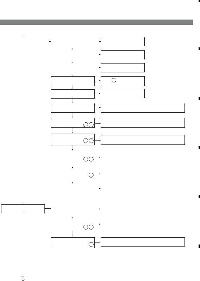
|
5 |
|
6 |
|
7 |
|
8 |
4.2.2 AUDIO SYSTEM
Flowchart of Failure Analysis for The Audio System
=> AU1 |
|
|
|
|
|
|
|
|
|
No |
|
|
|
Yes |
|
|
|
|
|
||||
Has the sound been emitted from |
|
Is sound muting set? |
|||||
the speakers? |
|
|
|
|
|||
|
|
|
|
|
|
||
|
|
|
|
|
|
|
|
|
Yes |
|
|
No |
|||
|
|
|
|
|
|
Yes |
|
|
|
|
|
Is the volume set to 0? |
|||
|
|
|
|
|
|
||
|
|
|
|
|
|
|
|
|
|
|
|
|
No |
||
|
|
|
|
|
|
No |
|
|
|
|
|
Is not headphone inserted? |
|||
|
|
|
|
|
|
||
|
|
|
|
||||
|
|
|
|
|
|
|
|
|
|
|
|
|
Yes |
||
Cancel muting, then check again.
Raise the volume, then check again.
Pull out headphone, then check again.
Sound of all functions does not output?
Yes
Check the speakers and speaker cables. Is it no problem?
Yes
Is a voltage (+16.5 V) supplied to IC9201?
Yes
Is not a signal output from CN9251? (pins 2, 4, 5, 7) 42 43
Yes
Is not a PWM signal output from IC9201?
(pins 34, 38, 46, 50)
Yes
No
No
No
No
No
Go to A .
Replace the speakers or speaker cables.
Check the cables (CN8806) from the main power and peripheral circuit. Repair the failure points.
Check the CN9251 and peripheral circuit.
Repair the failure points.
Check between the LPF (L9255, L9256) and CN9251. Repair the failure points.
A
B
C
Has the sound been emitted from No the Audio out terminal?
Yes
Is not a PWM signal output from |
No |
|
|
|||
|
Check the IC9101 and peripheral circuit. |
|||||
IC9101? |
46 |
47 |
|
|||
(pins 52, 53, 54, 55) |
|
|
Repair the failure points. |
|||
|
|
|
|
|
||
|
|
|
|
|
|
|
|
Yes |
|
|
|
|
|
|
|
|
|
|
|
|
|
|
|
|
|
|
|
Is a signal input to IC9101? |
|
No |
|
Check between the input terminals and IC9101. |
||
(pins 24, 25) |
|
48 |
|
|
Repair the failure points. |
|
|
|
|
|
|
|
|
|
Yes |
|
|
|
|
|
|
|
|
|
|
|
|
|
|
|
|
|
||
Has I2C communication signal |
|
No |
|
Check the peripheral circuits, the communication with the microcomputer |
||
arrived at IC9101? |
|
|
|
|
and X9101 clock output. If there was no ploblem replace the MSP5651M. |
|
|
|
|
|
|
||
|
|
|
|
|
|
|
|
|
|
|
|
|
|
Is a 12 V output from +12V_Reg |
|
|
Check the IC9181 and peripheral circuit. |
|||
output of IC9181 normal? |
|
|
|
|
Repair the failure points. |
|
|
|
|
|
|
|
|
|
Yes |
|
|
|
|
|
|
|
|
|
|
|
|
|
|
|
|
|
||
Are signals input to IC9151? |
|
|
|
Check the peripheral circuits and the communication with the |
||
(pins 2, 3, 5, 6) |
49 |
50 |
|
|
microcomputer. If there was no ploblem replace the MSP5651M. |
|
|
|
|
|
|
||
|
|
|
|
|
|
|
Yes
D
E
Are signals output from IC9151?
(pins 1, 7)
51
Check the IC9151 and peripheral circuit. Repair the failure points.
F
B
|
27 |
|
PDP-508XG |
||
|
|
5 |
|
6 |
|
7 |
|
8 |
|
|
|
|
|
|
||||
|
|
|
|
|

|
1 |
|
2 |
|
3 |
|
4 |
|
A B
Has the sound been emitted from No the Headphones?
Is sound muting set?
No
Is the volume set to 0?
No
Yes Cancel muting, then check again.
Yes Raise the volume, then check again.
|
|
Is a signal output from IC9101? |
No |
|
|
|
||
|
|
|
|
|
||||
|
|
(pins 38, 39) |
|
|
Check around the IC9101 and repair the failure points. |
|||
|
|
52 |
|
|
||||
|
|
|||||||
|
|
|
|
|
|
|
|
|
|
|
|
|
|
|
|
|
|
B |
|
|
|
Yes |
|
|
|
|
|
|
|
|
|
|
|
|
|
|
|
|
|
|
|
|
|
|
|
|
Is a signal output from IC8871? |
No |
Check the communications around the IC8871 and between the IC8871 |
||||
|
|
(pins 1, 7) |
53 |
|
|
and the microcomputer. If there was no ploblem, replace BH3544F. |
||
|
|
|
|
|||||
|
|
|
|
|
|
|
|
|
|
|
|
|
|
|
|
|
|
|
|
|
|
Yes |
|
|
|
|
|
|
|
|
|
|
|
|
|
|
|
|
|
|
|
|
||
|
|
Check the cables between CN8802 |
NG |
|
|
|
||
|
|
|
Replace the cables or SIDE IO Assy. |
|
||||
|
|
and CN9352 or check around the |
|
|
||||
|
|
|
|
|
||||
|
|
Headphones jack. |
|
|
|
|
|
|
|
|
|
|
|
|
|
|
|
C
 Waveforms
Input signal: L/R 1 kHz, 0.5 Vrms (VOL 30)
|
42 CN9251 - pins 2, 4 |
43 CN9251 - pins 5, 7 |
44 IC9201 - pins 34, 38 |
45 IC9201 - pins 44, 52 |
46 IC9101 - pins 52, 53 |
|
V: 2 V/div H: 1 mS/div |
V: 2 V/div H: 1 mS/div |
V: 10 V/div H: 5 μS/div |
V: 10 V/div H: 5 μS/div |
V: 2 V/div H: 5 μS/div |
D
|
47 IC9101 - pins 54, 55 |
48 IC9101 - pins 24, 25 |
49 IC9151 - pins 2, 3 |
50 IC9151 - pins 5, 6 |
51 IC9151 - pin 1, etc. |
|
V: 2 V/div H: 5 μS/div |
V: 2 V/div H: 1 mS/div |
V: 2 V/div H: 1 mS/div |
V: 2 V/div H: 1 mS/div |
V: 2 V/div H: 1 mS/div |
|
|
|
|
|
|
|
|
|
|
|
|
E |
52 IC9101 - pins 38, 39 |
53 IC8871 - pins 1, 7 |
V: 1 V/div H: 1 mS/div |
V: 1 V/div H: 1 mS/div |
|
|
|
|
|
|
|
F
28 |
|
|
PDP-508XG |
|
|
|
|
|||
|
1 |
|
2 |
|
|
|
3 |
|
4 |
|
|
|
|
|
|
|
|
||||
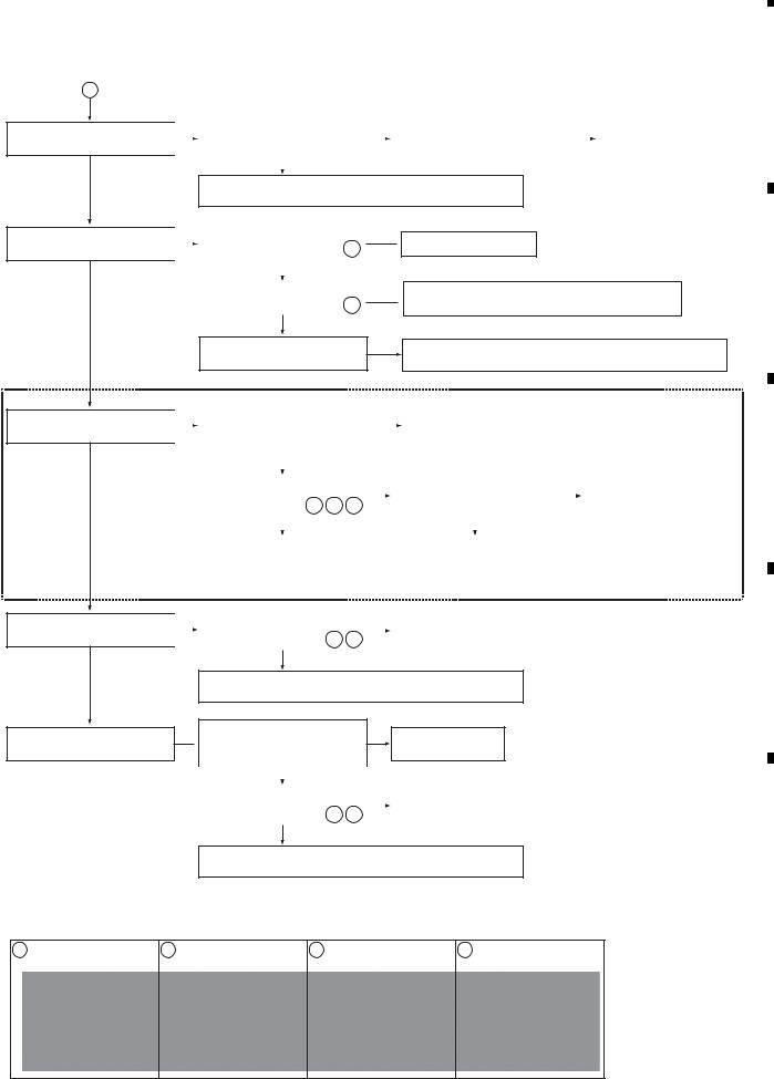
|
5 |
|
6 |
|
7 |
|
8 |
A
Has the sound of the Analog broadcasting output?
Yes
Has the sound of the HDMI output?
Yes
Has the sound of the Digital broadcasting output?
Yes
Has the sound of the analog RCA and PC inputs output?
Yes
Has the sound of the side input output?
|
No |
Is a SIF signal input to IC9101? |
No |
Check the communications between |
NG |
|
Replace the U6001 and |
|||
|
|
|||||||||
|
|
|
(pin 68) |
|
|
the U6001 and the microcomputer |
|
|
repair the failure points. |
|
|
|
|
|
|
||||||
|
|
|
|
|
|
|
and between the U6001 and IC9101. |
|
|
|
|
|
|
|
|
|
|
|
|
|
|
|
|
|
|
|
|
|
|
|
|
|
|
|
|
|
Yes |
|
|
|
|
|
|
Check the communications around the IC9101 and between the IC9101 and the microcomputer. If there was no ploblem, replace MSP5651M.
No |
Is a SPDIF signal output from |
54 |
||
|
|
IC5201? (pin 78) |
||
|
|
|
|
|
|
|
|
Yes |
|
|
|
|
|
|
|
|
Is a SPDIF signal input to |
|
|
|
|
IC9101? (pin 4) |
54 |
|
|
|
|
|
|
Yes
Check that the HDMI switch of the MENU is properly set.
No
No
NG
 Replace the IC5201.
Poor contact of the connector or FFC, or cable is defective.  Replace FFC or cable.
Check the communications around the IC9101 and between the IC9101 and the microcomputer. If there was no ploblem, replace MSP5651M.
|
|
|
Check the FFC and cables between |
|
|
|
|
|
|
|
|
|
|
|
|
||
|
No |
the MAIN Assy and TANSHI Assy. |
|
Yes |
Poor contact of the connector or |
|
|
|
|
|
|||||||
|
|
FFC, or cable is defective. |
|
|
|
|
|
||||||||||
|
|
|
Does not sound output even if replace |
|
|
|
|
|
|
|
|
|
|
||||
|
|
|
|
|
|
|
|
Replace FFC or cable. |
|
|
|
|
|
||||
|
|
|
them? |
|
|
|
|
|
|
|
|
|
|
||||
|
|
|
|
|
|
|
|
|
|
|
|
|
|
|
|||
|
|
|
|
|
|
|
|
|
|
|
|
|
|
|
|
|
|
|
|
|
|
No |
|
|
|
|
|
|
|
|
|
|
|
|
|
|
|
|
|
|
|
|
|
|
|
|
|
|
|
|
|
|
|
|
|
|
Is a I2S signal input to IC9101? |
|
No |
Is a signal output from IC8401 of |
No |
|
|
|
|
||||||
|
|
|
|
|
Repare the DTB block. |
||||||||||||
|
|
|
(pins 106 to 108) |
|
|
||||||||||||
|
|
|
|
|
|
|
the MAIN Assy? |
|
|||||||||
|
|
|
55 56 57 |
|
|
|
|
|
|
|
|
|
|||||
|
|
|
|
|
|
|
|
|
|
|
|
|
|
|
|
||
|
|
|
|
Yes |
|
|
|
|
|
|
Yes |
|
|
|
|
|
|
|
|
|
|
|
|
|
|
|
|
|
|
|
|
||||
|
|
|
Check the communications around the |
|
|
|
Check around IC8401 and repair |
|
|
|
|
|
|||||
|
|
|
IC9101 and between the IC9101 and |
|
|
|
the failure points. |
|
|
|
|
|
|||||
|
|
|
the microcomputer. If there was no |
|
|
|
|
|
|
|
|
|
|
|
|
||
|
|
|
ploblem replace the MAIN Assy. |
|
|
|
|
|
|
|
|
|
|
DTV model only |
|
||
|
|
|
|
|
|
|
|
|
|
|
|
|
|
|
|
||
|
|
|
|
|
|
|
|
|
|
|
|
|
|
|
|
||
|
No |
Is a signal input to IC9101? |
|
No |
|
|
|
|
|
|
|
|
|
||||
|
Check between input terminal and |
|
|
|
|
|
|||||||||||
|
(pins 24 to 27, 32 to 35) |
|
|
|
|
|
|
||||||||||
|
|
|
49 50 |
|
|
|
|
IC9101 and repair the failure points. |
|
|
|
|
|
||||
|
|
|
|
|
|
|
|
|
|
|
|
|
|
|
|
|
|
Yes
Check the communications around the IC9101 and between the IC9101 and the microcomputer. If there was no ploblem replace the MAIN Assy.
Check the cables between CN8801
No and CN9351, and check around NG Replace the cables. the pin jack.
|
OK |
|
|
|
|
|
|
|
|
Is a signal input to IC9101? |
No |
Check between IC9101 and |
||
(pins 30, 31) |
49 50 |
|
|
CN8801 and repair the failure points. |
|
||||
|
|
|
|
|
|
|
|
|
|
Yes
Check the communications around the IC9101 and between the IC9101 and the microcomputer. If there was no ploblem replace the MAIN Assy.
A
B
C
D
E
 Waveforms
Input signal: L/R 1 kHz, 0.5 Vrms (VOL 30)
54 IC5201 - pin 78 |
μS/div |
55 IC9101 - pin 106 |
μS/div |
56 IC9101 - pin 107 |
μS/div |
57 IC9101 - pin 108 |
μS/div |
|
|
||||||||
V: 1 V/div H: 1 |
V: 1 V/div H: 10 |
V: 1 V/div H: 10 |
V: 1 V/div H: 10 |
|
F
|
29 |
|
PDP-508XG |
||
|
|
5 |
|
6 |
|
7 |
|
8 |
|
|
|
|
|
|
||||
|
|
|
|
|

|
30 |
|
F |
|
|
|
E |
|
|
|
|
D |
|
|
C |
|
B |
|
|
A |
|
|
|
|
|
|
|
|
|
|
|
|
|
|
|
|
|
|
|
|
|
|
|
|
|
|
|
|
|
|
|
|
|
|
|
|
|
|
|
|
||
|
|
|
Frequency of |
Major Type |
Detailed Type |
Log Indication in Factory Mode |
Checkpoint |
Possible Defective |
|
Remarks |
|
|||||||||
|
|
|
LED Flashing |
MAIN |
|
SUB |
Part |
|
|
|||||||||||
|
|
|
|
|
|
|
|
|
|
|
|
|
|
|
|
|||||
|
|
|
|
|
|
|
|
|
|
|
|
|
|
|
|
|
|
|||
1 |
|
|
|
|
|
|
Communication error |
|
|
|
RTRY |
CLK_SQ/TXD_SQ, etc. |
IC3401, IC3151 |
SQ_IC communication not established. IC3401 may not have properly started up. |
||||||
|
|
|
|
Abnormality in the |
Drive stop |
SQ-LSI |
|
SQNO |
Check if the video sync signal is input to IC3401. |
CN3001, IC3001,IC3401 |
A shutdown occurs if IC3401 has not properly started up (a communication failure between IC3401 and IC3306 [FLASH]). |
|||||||||
|
|
|
Blue 1 |
Busy |
|
BUSY |
BUSY_SQ |
IC3401, IC3151 |
If BUSY_SQ remains high, a shutdown is generated. |
|
||||||||||
|
|
|
Sequence LSI |
|
|
|
|
|||||||||||||
|
|
|
|
Incoherent version (hardware, software) |
|
|
|
VER-HS |
Check the model number of the DIGITAL Assy and the destination of SEQ-PROS. |
IC3306, IC3151 |
The written SEQ-PROG is incoherent with data on the DIGITAL Assy. |
|
||||||||
|
|
|
|
|
|
|
|
|
|
|
||||||||||
|
|
|
|
|
|
|
Incoherent version (memory, |
|
|
|
VER-MS |
Check the model number of the DIGITAL Assy and the |
IC3306, IC3151 |
A shutdown occurs if the SEQ-PROG that has been stored in backup |
|
|||||
|
|
|
|
|
|
|
software) |
|
|
|
|
destination of SEQ-PROS. |
|
memory does not coincide with the actual SEQ-PROG. |
|
|||||
|
|
|
|
Failure in IIC |
DIGITAL Assy EEPROM |
|
|
|
EEPROM |
IIC communication line of IC3156 |
IC3156, IC3151 |
Check the pull-up resistor of the IIC control line and the power to the corresponding IC. |
||||||||
|
|
|
Blue 2 |
SENSOR Assy EEPROM |
|
|
|
BACKUP |
IIC communication line of IC3652 |
IC3652, IC3151 |
Check the pull-up resistor of the IIC control line and the power to the corresponding IC. |
|||||||||
|
|
|
communication with the |
MD-IIC |
|
|||||||||||||||
|
|
|
|
module microcomputer |
DAC1 |
|
|
|
DAC1 |
IIC communication line of IC3157 |
IC3157, IC3151 |
Check the pull-up resistor of the IIC control line and the power to the corresponding IC. |
||||||||
|
|
|
|
|
|
|||||||||||||||
|
|
|
|
|
|
|
DAC2 |
|
|
|
DAC2 |
IIC communication line of IC3158 |
IC3158, IC3151 |
Check the pull-up resistor of the IIC control line and the power to the corresponding IC. |
||||||
|
|
|
Blue 3 |
Abnormality in RST2 |
– |
RST2 |
|
– |
Is the output voltage of the DC-DC converter low? |
IC3602(BD9302FP) |
If RST2 does not become high after the unit is turned on, a shutdown will be generated in several seconds. |
|||||||||
|
|
|
power decrease |
|
The 12 V power is not output. |
POWER SUPPLY Unit,FU3601 |
Check if V + 12 V is started. Also check if the FU3601 on the DIGITAL Assy has been melted. |
|||||||||||||
|
|
|
|
|
|
|
|
|
||||||||||||
|
|
|
|
|
|
|
|
|
|
|
TMP-H |
High temperature abnormality in the panel temperature sensor |
SENSOR Assy (IC3651) |
° |
|
|
|
|||
|
|
|
Blue 4 |
Abnormality in panel |
– |
TMP-NG |
|
|
|
|
|
|
If TEMP1 that is read by the module microcomputer is 75 C or higher, a shutdown will be generated. |
|||||||
|
|
|
|
|
|
|
|
|
A shutdown occurs if the reading of TEMP1 detected by the module microcomputer is |
|||||||||||
|
|
|
temperature |
|
TMP-L |
Low temperature abnormality in the panel temperature sensor |
SENSOR Assy (IC3651) |
|||||||||||||
|
|
|
|
|
|
|
|
–20°C or less. Also check the connection with the SENSOR Assy. |
|
|||||||||||
|
|
|
|
|
|
|
|
|
|
|
|
|
|
|
|
|
||||
2 |
|
|
|
Short-circuiting of the |
|
|
|
|
|
Speaker terminals |
JA9301 |
Check if any speaker cable is in contact with the chassis. |
|
|||||||
|
|
Blue 5 |
speakers / D-AMP |
– |
AUDIO |
|
– |
AUDIO_AMP |
IC9201, IC9101 |
Check if the AMP output is short-circuited. |
|
|||||||||
|
|
|
|
|
||||||||||||||||
|
|
|
|
temperature abnormality |
|
|
|
|
|
Periphery of the cable between IO3 and M8, and IO6 and P5 |
CN8803,CN4001,CN8806,P5 |
Check if cables are firmly connected. |
|
|||||||
|
|
|
|
|
|
|
|
|
|
|
|
|
|
|||||||
|
|
|
Blue 6 |
Failure in communication with |
– |
MODULE |
|
– |
Communication line between MAIN and MOD |
IC3151, IC8401 |
Check the communication lines (TXD_MOD/RXD_MOD/REQ_MOD). |
|
||||||||
|
|
|
the module microcomputer |
|
Periphery of the cable between D11 and M1 |
CN3001, CN4101 |
Check if cables are firmly connected. |
|
||||||||||||
|
|
|
|
|
|
|
|
|
|
|||||||||||
|
-PDP |
|
|
Failure in main |
IF microcomputer |
MA-3L |
|
IF |
Communication line between IF and MAIN |
IC8301, IC8401 |
Check the communication lines (TXD_IF/RXD_IF/CLK_IF/BUSY_IF/CE_IF/REQ_IF). |
|||||||||
|
|
Blue 7 |
microcomputer 3-wire |
|
|
|
|
|
|
|
|
|
|
|
|
|||||
|
|
|
MULTI processor |
|
MULTI |
Communication line between MULTI and MAIN |
IC8001, IC8401 |
Check the communication lines (TXD_IC3/RXD_IC3). |
|
|||||||||||
|
|
|
|
serial communication |
|
|
|
|
||||||||||||
|
508XG |
|
|
|
|
|
|
|
|
|
|
|
|
|
|
|
|
|
|
|
|
|
|
|
|
|
Tuner 1 |
|
|
|
FE1 |
IIC communication line between Tuner and MAIN |
U6001,IC8401,IC6101 |
Check the communication lines (SCL_TU/SDA_TU or SCL_AV5/SDA_AV5). |
|||||||
|
|
|
|
|
|
|
|
|
|
|||||||||||
|
|
|
|
|
|
|
MSP/MAP |
|
|
|
MSPMAP |
IIC communication line between MSP/MAP and MAIN |
IC9101, IC8401 |
Check the communication lines (SCL_AV/SDA_AV). |
|
|||||
|
|
|
|
|
|
|
AV switch |
|
|
|
AV-SW |
IIC communication line between AV-SW and MAIN |
IC4601, IC8401 |
Check the communication lines (SCL_AV5/SDA_AV5). |
|
|||||
|
|
|
|
Failure in IIC |
RGB switch |
MA-IIC |
|
RGB-SW |
IIC communication line between RGB-SW and MAIN |
IC4701, IC8401 |
Check the communication lines (SCL_AV5/SDA_AV5). |
|
||||||||
|
|
|
Blue 8 |
communication with the |
VDEC |
|
|
|
VDEC |
IIC communication line between M-VDEC and MAIN |
IC4801, IC8401 |
Check the communication lines (SCL_MB/SDA_MB). |
|
|||||||
|
|
|
|
main microcomputer |
VDEC SDRAM |
|
|
|
SDRAM |
IIC communication line between VDEC and SDRAM |
IC4801, IC4802 |
Check the communication lines (SDRAM). Defective SDRAM |
|
|||||||
|
|
|
|
|
|
|
|
|
|
|
||||||||||
|
|
|
|
|
|
|
AD/PLL |
|
|
|
ADC |
IIC communication line between ADC and MAIN |
IC5001, IC8401 |
Check the communication lines (SCL_AV/SDA_AV). |
|
|||||
|
|
|
|
|
|
|
|
|
|
|
|
|
|
|
|
|||||
|
|
|
|
|
|
|
HDMI |
|
|
|
HDMI |
IIC communication line between HDMI_RX and MAIN |
IC5201, IC8401 |
Check the communication lines (SCL_MB/SDA_MB). |
|
|||||
3 |
|
|
|
|
|
|
|
|
|
|
|
|
|
|
|
|
|
|
|
|
|
|
|
|
|
|
|
|
|
|
|
|
|
|
|
|
|
|
|
||
|
|
|
Blue 9 |
Failure in communication |
– |
MAIN |
|
– |
Communication line between IF and MAIN |
IC8301, IC8401 |
Check the communication lines (TXD_IF/RXD_IF/CLK_IF/BUSY_IF/CE_IF/REQ_IF). |
|||||||||
|
|
|
with the main microcomputer |
|
||||||||||||||||
|
|
|
|
|
|
|
|
|
|
|
|
|
|
|
|
|
|
|||
|
|
|
|
|
|
|
|
|
|
|
|
|
|
|
|
|||||
|
|
|
|
|
|
|
|
|
|
|
|
Dirt attached to the fan motor |
– |
Check the fan(AXM1057). |
|
|||||
|
|
|
Blue 10 |
FAN NG |
FAN1 |
FAN |
|
FAN1 |
Periphery of the FAN CONNECT |
AWW1290, AWW1329 |
FAN NG |
|
||||||||
|
|
|
|
|
|
|
|
|
|
|
|
Periphery of the cable between FA1 and M5, FAN and M4, and FA2 and FA5 |
CN9551 to CN9555,CN4103,CN4108 |
Check if cables are firmly connected. |
|
|||||
|
|
|
|
|
|
|
|
|
|
|
|
Periphery of the fan control regulator |
IC4310, IC4303 |
|
– |
|
||||
|
|
|
|
High temperature of the |
|
|
|
|
|
Temperature sensor or its periphery |
– |
TEMP2 A shutdown occurs because of high temperature. |
|
|||||||
|
|
|
Blue 11 |
– |
TEMP2 |
|
– |
Periphery of the temperature sensor |
TH9091 |
TEMP2 |
|
|||||||||
|
|
|
unit |
|
|
|||||||||||||||
|
|
|
|
|
|
|
|
|
Periphery of the cable between IO4 and M6 |
CN8804, CN4004 |
Check if cables are firmly connected. |
|
||||||||
|
|
|
|
|
|
|
|
|
|
|
|
|
||||||||
|
|
|
Blue 12 |
Digital Tuner |
DTV startup error |
DTUNER |
|
PS/RST |
– |
IC8401 |
Check if DTV antenna is short-circuited. |
|
||||||||
|
|
|
(PDP-508XDA only) |
DTV communication error |
|
RETRY |
– |
– |
|
– |
|
|||||||||
|
|
|
|
|
|
|
|
|
||||||||||||
|
|
|
|
|
|
|
|
|
|
|
|
|||||||||
|
|
|
|
|
|
|
DC-DC Converter power decrease |
|
|
|
M-DCDC |
DC-DC converter or its periphery, RST2 |
IC4403, Q4404 |
Check if V + 3.3 V_D4 is started. |
|
|||||
|
|
|
|
|
|
|
|
|
|
EMG_USB |
IC4309 |
Check if the voltage at a waveform check point is 5 V. |
|
|||||||
|
|
|
|
|
|
|
|
|
|
|
|
|
||||||||
|
|
|
Blue 13 |
Failure in the power |
|
RST-MA |
|
|
The 12 V power is not output, RST4 |
POWER SUPPLY Unit |
Check if V + 12 V is started. |
|
||||||||
4 |
|
|
supply |
|
|
|
|
|
The 6.5 V power is not output |
POWER SUPPLY Unit |
Check if V + 6.5 V is started. |
|
||||||||
|
|
|
|
|
|
|
POWER SUPPLY |
|
|
|
RELAY |
|
||||||||
|
|
|
|
|
|
|
|
|
|
The 5.1 V power is not output |
POWER SUPPLY Unit |
Check if V + 5.1 V is started. |
|
|||||||
|
|
|
|
|
|
|
|
|
|
|
|
|
||||||||
|
|
|
|
|
|
|
|
|
|
|
|
EMG_DDC |
DCDC converter |
Check if the DCDC converter is overloaded. |
|
|||||
|
|
|
|
|
|
|
|
|
|
|
|
Periphery of the cable between P8 and M3 |
CN4105 |
Check if cables are firmly connected. |
|
|||||
|
|
|
Blue 15 |
Main EEPROM |
Main EEPROM communication error |
MA-EEP |
|
– |
IIC communication line between EEPROM and MAIN |
IC8404, IC8401 |
Check the communication lines (SCL_EP/SDA_EP). |
|
||||||||
|
|
|
|
|
|
|
|
|
|
|
|
|
|
|
|
|
|
|
|
|
|
|
|
|
|
|
|
|
|
|
|
|
|
|
|
|
|
|
|
|
|
.3.4 |
3.4 |
1 |
OF DIAGNOSIS |
(SHUTDOWN) SD |
|
DIAGNOSIS |
(SHUTDOWN) SD |
1
2
3
4
Loading...