


 Loading...
ORDER NO.
ARP3464
PDP-LX5080D
PLASMA TELEVISION
PDP-LX5080D
PDP-LX508D
THIS MANUAL IS APPLICABLE TO THE FOLLOWING MODEL(S) AND TYPE(S).
Model |
Type |
Power Requirement |
Remarks |
||||
|
|
|
|
|
|
|
|
PDP-LX5080D |
YVIXK5 |
AC 220 V to 240 V |
|
||||
|
|
|
|
|
|
|
|
PDP-LX508D |
WYVIXK5 |
AC 220 V to 240 V |
|
||||
|
|
|
|
|
|
|
|
PDP-LX508D |
WYV5 |
AC 220 V to 240 V |
|
||||
|
|
|
|
|
|
|
|
|
|
|
|
|
|
|
|
|
|
|
|
|
|
|
|
|
|
|
|
|
|
|
|
For details, refer to "Important Check Points for good servicing".
PIONEER CORPORATION 4-1, Meguro 1-chome, Meguro-ku, Tokyo 153-8654, Japan
PIONEER ELECTRONICS (USA) INC. P.O. Box 1760, Long Beach, CA 90801-1760, U.S.A.
PIONEER EUROPE NV Haven 1087, Keetberglaan 1, 9120 Melsele, Belgium
PIONEER ELECTRONICS ASIACENTRE PTE. LTD. 253 Alexandra Road, #04-01, Singapore 159936
 PIONEER CORPORATION 2007
T-IZS-001 AUG. 2007 Printed in Japan

|
1 |
|
2 |
|
3 |
|
4 |
|
SAFETY INFORMATION
A
This service manual is intended for qualified service technicians ; it is not meant for the casual do-it-yourselfer. Qualified technicians have the necessary test equipment and tools, and have been trained to properly and safely repair complex products such as those covered by this manual.
Improperly performed repairs can adversely affect the safety and reliability of the product and may void the warranty. If you are not qualified to perform the repair of this product properly and safely, you should not risk trying to do so and refer the repair to a qualified service technician.
WARNING
BThis product contains lead in solder and certain electrical parts contain chemicals which are known to the state of California to cause cancer, birth defects or other reproductive harm.
Health & Safety Code Section 25249.6 - Proposition 65
NOTICE
(FOR CANADIAN MODEL ONLY)
Fuse symbols 


 (fast operating fuse) and/or


 (slow operating fuse) on PCB indicate that replacement parts must be of identical designation.
REMARQUE |
|
|
(POUR MODÈLE CANADIEN SEULEMENT) |
|
|
Les symboles de fusible |
(fusible de type rapide) et/ou |
(fusible de type lent) sur CCI indiquent que les pièces |
C |
de remplacement doivent avoir la même désignation. |
|
SAFETY PRECAUTIONS
NOTICE : Comply with all cautions and safety related notes located on or inside the cabinet and on the chassis.
The following precautions should be observed :
1. When service is required, even though the PDP UNIT an
Disolation transformer should be inserted between the power line and the set in safety before any service is performed.
2.When replacing a chassis in the set, all the protective devices must be put back in place, such as barriers, nonmetallic knobs, adjustment and compartment covershields, isolation resistorcapacitor, etc.
3. When service is required, observe the original lead dress. Extra precaution should be taken to assure correct lead dress in the high voltage circuitry area.
4. Always use the manufacture's replacement components. Especially critical components as indicated on the circuit diagram should not be replaced by other manufacture's.
EFurthermore where a short circuit has occurred, replace those components that indicate evidence of overheating.
5.Before returning a serviced set to the customer, the service technician must thoroughly test the unit to be certain that it is completely safe to operate without danger of electrical shock, and be sure that no protective device built into the set by the manufacture has become defective, or inadvertently defeated during servicing. Therefore, the following checks should be performed for the continued protection of the customer and servicetechnician.
6.Perform the following precautions against unwanted radiation and rise in internal temperature.
•Always return the internal wiring to the original styling.
•Attach parts (Gascket, Ferrite Core, Ground, Rear Cover, Shield Case etc.) surely after disassembly.
7. Perform the following precautions for the PDP panel.
•When the front case is removed, make sure nothing hits the panel face, panel corner, and panel edge (so that the glass does not break).
•Make sure that the panel vent does not break. (Check that the cover is attached.)
•Handle the FPC connected to the panel carefully. Twisting or pulling the FPC when connecting it to the
connector will cause it to peel off from the panel. 8. Pay attention to the following.
•Pay extreme caution when the front case and rear panel are removed because this may cause a high risk of disturbance to TVs and radios in the surrounding.
F
2 |
|
|
PDP-LX5080D |
|
|
|
|
|||
|
1 |
|
2 |
|
|
|
3 |
|
4 |
|
|
|
|
|
|
|
|
||||

|
5 |
|
6 |
Leakage Current Cold Check
With the AC plug removed from an AC power source, place a jumper across the two plug prongs. Turn the AC power switch on. Using an insulation tester (DC 500V), connect one lead to the jumpered AC plug and touch the other lead to each exposed metal part (input/output terminals, screwheads, metal overlays, control shafts, etc.), particularly any exposed metal part having a return path to the chassis. Exposed metal parts having a return path to the chassis should have a minimum resistor reading of 4 MΩ.
The below 4 MΩ resistor value indicate an abnormality which require corrective action. Exposed metal parts not having a return path to the chassis will indicate an open circuit.
Leakage Current Hot Check
Plug the AC line cord directly into an AC power source (do not use an isolation transformer for this check).
Turn the AC power switch on.
U s i n g a " L e a k a g e C u r r e n t Te s t e r ( S i m p s o n M o d e l 2 2 9 equivalent)", measure for current from all exposed metal parts of the cabinet (input/output terminals, screwheads, metal overlays, control shaft, etc.), particularly any exposed metal part having a return path to the chassis, to a known earth ground (water pipe, conduit, etc.). Any current measured must not exceed 1 mA.
|
7 |
|
|
8 |
A |
|
PRODUCT SAFETY NOTICE |
|
|||
|
|
|
|||
|
Many electrical and mechanical parts in PIONEER set have |
|
|||
|
special safety related characteristics. These are often not evident |
|
|||
|
from visual inspection nor the protection afforded by them |
|
|||
|
necessarily can be obtained by using replacement components |
|
|||
|
rated for higher voltage, wattage, etc. Replacement parts which |
|
|||
|
|
||||
|
have these special safety characteristics are identified in this |
|
|||
|
Service Manual. |
|
|
||
|
Electrical components having such features are identified by |
|
|||
|
marking with a >on the schematics and on the parts list in this |
|
|||
|
Service Manual. |
|
|
||
|
The use of a substitute replacement component which dose not |
B |
|||
|
h a v e t h e s a m e s a f e t y c h a r a c t e r i s t i c s a s t h e P I O N E E R |
|
|||
|
recommended replacement one, shown in the parts list in this |
|
|||
|
Service Manual, may create shock, fire or other hazards. |
|
|||
|
Product Safety is continuously under review and new instructions |
|
|||
|
are issued from time to time. For the latest information, always |
|
|||
|
consult the current PIONEER Service Manual. A subscription to, |
|
|||
|
|
||||
|
or additional copies of, PIONEER Service Manual may be |
|
|||
|
obtained at a nominal charge from PIONEER. |
|
|
||
C
|
|
Reading should |
|
Leakage |
not be above |
Device |
current |
1 mA |
under |
tester |
|
test |
|
|
Test all |
|
|
exposed metal |
|
|
surfaces |
|
|
|
|
D |
Also test with |
|
|
plug reversed |
|
Earth |
(Using AC adapter |
|
ground |
plug as required) |
|
|
AC Leakage Test
A N Y M E A S U R E M E N T S N OT W I T H I N T H E L I M I T S
OUTLINED ABOVE ARE INDICATIVE OF A POTENTIAL
SHOCK HAZARD AND MUST BE CORRECTED BEFORE
RETURNING THE SET TO THE CUSTOMER.
E
F
|
3 |
|
PDP-LX5080D |
||
|
|
5 |
|
6 |
|
7 |
|
8 |
|
|
|
|
|
|
||||
|
|
|
|
|
|
1 |
|
2 |
|
3 |
|
4 |
|
A
[Important Check Points for Good Servicing]
In this manual, procedures that must be performed during repairs are marked with the below symbol. Please be sure to confirm and follow these procedures.
1. Product safety
Please conform to product regulations (such as safety and radiation regulations), and maintain a safe servicing environment by following the safety instructions described in this manual.
1 Use specified parts for repair.
Use genuine parts. Be sure to use important parts for safety.
2 Do not perform modifications without proper instructions.
B
Please follow the specified safety methods when modification(addition/change of parts) is required due to interferences such as radio/TV interference and foreign noise.
3 Make sure the soldering of repaired locations is properly performed.
When you solder while repairing, please be sure that there are no cold solder and other debris.
Soldering should be finished with the proper quantity. (Refer to the example)
4 Make sure the screws are tightly fastened.
Please be sure that all screws are fastened, and that there are no loose screws.
5 Make sure each connectors are correctly inserted.
Please be sure that all connectors are inserted, and that there are no imperfect insertion.
C
6 Make sure the wiring cables are set to their original state.
Please replace the wiring and cables to the original state after repairs.
In addition, be sure that there are no pinched wires, etc.
7Make sure screws and soldering scraps do not remain inside the product. Please check that neither solder debris nor screws remain inside the product.
8There should be no semi-broken wires, scratches, melting, etc. on the coating of the power cord.
Damaged power cords may lead to fire accidents, so please be sure that there are no damages.
If you find a damaged power cord, please exchange it with a suitable one.
9 There should be no spark traces or similar marks on the power plug.
D
When spark traces or similar marks are found on the power supply plug, please check the connection and advise on secure connections and suitable usage. Please exchange the power cord if necessary.
a Safe environment should be secured during servicing.
When you perform repairs, please pay attention to static electricity, furniture, household articles, etc. in order to prevent injuries. Please pay attention to your surroundings and repair safely.
2. Adjustments
 To keep the original performance of the products, optimum adjustments and confirmation of characteristics within specification. Adjustments should be performed in accordance with the procedures/instructions described in this manual.
E
3. Lubricants, Glues, and Replacement parts |
Use grease and adhesives that are equal to the specified substance. |
Make sure the proper amount is applied. |
4. Cleaning |
 For parts that require cleaning, such as optical pickups, tape deck heads, lenses and mirrors used in projection monitors, proper cleaning should be performed to restore their performances.
5. Shipping mode and Shipping screws
F |
|
To protect products from damages or failures during transit, the shipping mode should be set or the shipping screws should be |
|
|
installed before shipment. Please be sure to follow this method especially if it is specified in this manual. |
|
|
4 |
|
|
PDP-LX5080D |
|
|
|
|
|||
|
1 |
|
2 |
|
|
|
3 |
|
4 |
|
|
|
|
|
|
|
|
||||

|
5 |
|
|
6 |
|
|
7 |
|
8 |
CONTENTS |
|
|
|
|
|
|
|||
|
SAFETY INFORMATION ......................................................................................................................................................... |
|
|
|
|
2 |
|||
|
1. SERVICE PRECAUTIONS.................................................................................................................................................... |
|
|
|
|
7 |
|||
|
1.1 NOTES ON SOLDERING ............................................................................................................................................... |
|
|
|
|
7 |
|||
|
1.2 CHARGED SECTION AND HIGH VOLTAGE GENERATING POINT |
............................................................................. |
8 |
||||||
|
2. SPECIFICATIONS................................................................................................................................................................. |
|
|
|
|
9 |
|||
|
2.1 ACCESSORIES.............................................................................................................................................................. |
|
|
|
|
9 |
|||
|
2.2 SPECIFICATIONS ........................................................................................................................................................ |
|
|
|
|
10 |
|||
|
2.3 PANEL FACILITIES....................................................................................................................................................... |
|
|
|
|
11 |
|||
|
3. BASIC ITEMS FOR SERVICE ............................................................................................................................................ |
|
|
|
|
14 |
|||
|
3.1 CHECK POINTS AFTER SERVICING ......................................................................................................................... |
|
|
|
|
14 |
|||
|
3.2 QUICK REFERENCE ................................................................................................................................................... |
|
|
|
|
15 |
|||
|
3.3 PCB LOCATION ........................................................................................................................................................... |
|
|
|
|
17 |
|||
|
3.4 JIGS LIST ..................................................................................................................................................................... |
|
|
|
|
18 |
|||
|
3.5 CLEANING ................................................................................................................................................................... |
|
|
|
|
18 |
|||
|
4. BLOCK DIAGRAM .............................................................................................................................................................. |
|
|
|
|
20 |
|||
|
4.1 OVERALL WIRING DIAGRAM (1/2)............................................................................................................................. |
|
|
|
|
20 |
|||
|
4.2 OVERALL WIRING DIAGRAM (2/2)............................................................................................................................. |
|
|
|
|
22 |
|||
|
4.3 OVERALL BLOCK DIAGRAM (1/2) .............................................................................................................................. |
|
|
|
|
24 |
|||
|
4.4 OVERALL BLOCK DIAGRAM (2/2) .............................................................................................................................. |
|
|
|
|
26 |
|||
|
4.5 POWER SUPPLY UNIT ................................................................................................................................................ |
|
|
|
|
28 |
|||
|
4.6 50F X DRIVE ASSY...................................................................................................................................................... |
|
|
|
|
29 |
|||
|
4.7 50F Y DRIVE, 50F SCAN A, B, C and D ASSYS ......................................................................................................... |
|
30 |
||||||
|
4.8 POWER SUPPLY BLOCK of 50F X, Y DRIVE and 50F SCAN A, B, C and D ASSYS ................................................ |
31 |
|||||||
|
4.9 50F ADDRESS L and S ASSYS................................................................................................................................... |
|
|
|
|
32 |
|||
|
4.10 50F DIGITAL ASSY .................................................................................................................................................... |
|
|
|
|
33 |
|||
|
4.11 POWER SUPPLY BLOCK of MAIN ASSY.................................................................................................................. |
|
34 |
||||||
|
4.12 TANSHI ASSY ............................................................................................................................................................ |
|
|
|
|
36 |
|||
|
4.13 50FHD LED, FHD IR and FHD RLS ASSYS .............................................................................................................. |
|
37 |
||||||
|
4.14 POWER SUPPLY BLOCK of 50LED&IR and SIDE KEY ASSYS............................................................................... |
|
38 |
||||||
|
5. DIAGNOSIS ........................................................................................................................................................................ |
|
|
|
|
39 |
|||
|
5.1 POWER SUPPLY OPERATION.................................................................................................................................... |
|
|
|
|
39 |
|||
|
5.1.1 LED DISPLAY INFORMATION............................................................................................................................... |
|
|
|
|
39 |
|||
|
5.1.2 POWER ON SEQUENCE ...................................................................................................................................... |
|
|
|
|
40 |
|||
|
5.1.3 DETAILS OF POWER ON SEQUENCE................................................................................................................. |
|
41 |
||||||
|
5.2 DIAGNOSIS FLOWCHART OF FAILURE ANALYSIS .................................................................................................. |
|
45 |
||||||
|
5.2.1 WHOLE UNIT......................................................................................................................................................... |
|
|
|
|
45 |
|||
|
5.2.2 POWER SUPPLY UNIT.......................................................................................................................................... |
|
|
|
|
47 |
|||
|
5.2.3 DRIVE ASSY.......................................................................................................................................................... |
|
|
|
|
48 |
|||
|
5.2.4 DIGITAL ASSY ....................................................................................................................................................... |
|
|
|
|
52 |
|||
|
5.2.5 MAIN ASSY............................................................................................................................................................ |
|
|
|
|
53 |
|||
|
5.2.6 VIDEO SYSTEM .................................................................................................................................................... |
|
|
|
|
54 |
|||
|
5.2.7 AUDIO SYSTEM .................................................................................................................................................... |
|
|
|
|
61 |
|||
|
5.3 DIAGNOSIS OF PD (POWER-DOWN) ........................................................................................................................ |
|
|
|
|
64 |
|||
|
5.3.1 BLOCK DIAGRAM OF THE POWER-DOWN SIGNAL .......................................................................................... |
|
64 |
||||||
|
5.3.2 PD (POWER-DOWN) DIAGNOSIS OF FAILURE ANALYSIS ................................................................................ |
|
65 |
||||||
|
5.4 DIAGNOSIS OF SD (SHUTDOWN) ............................................................................................................................. |
|
|
|
|
68 |
|||
|
5.4.1 BLOCK DIAGRAM OF THE SHUTDOWN SIGNAL ............................................................................................... |
|
68 |
||||||
|
5.4.2 SD (SHUTDOWN) DIAGNOSIS ............................................................................................................................. |
|
|
|
|
69 |
|||
|
5.5 NON-FAILURE INFORMATION.................................................................................................................................... |
|
|
|
|
71 |
|||
|
5.5.1 INFORMATION ON SYMPTOMS THAT DO NOT CONSTITUTE FAILURE .......................................................... |
71 |
|||||||
|
5.5.2 FUNCTION OF DECREASING THE BRIGHTNESS LEVEL ................................................................................. |
|
75 |
||||||
|
5.6 OUTLINE OF THE OPERATION ................................................................................................... |
|
|
............................... |
|
76 |
|||
|
5.6.1 PANEL DRIVE-POWER ON / OFF FUNCTION ..................................................................................................... |
|
76 |
||||||
|
5.6.2 SPECIFICATION OF THE FAN CONTROL............................................................................................................ |
|
77 |
||||||
|
5.6.3 PROCESSING IN ABNORMALITY ........................................................................................................................ |
|
|
|
|
78 |
|||
A
B
C
D
E
F
|
5 |
|
PDP-LX5080D |
||
|
|
5 |
|
6 |
|
7 |
|
8 |
|
|
|
|
|
|
||||
|
|
|
|
|
|
1 |
|
|
2 |
|
|
3 |
|
4 |
|
|
6. SERVICE FACTORY MODE................................................................................................................................................ |
|
|
|
|
81 |
|
|||
|
6.1 OUTLINE OF THE SERVICE FACTORY MODE .......................................................................................................... |
|
81 |
|
||||||
|
6.1.1 SERVICE FACTORY MODE TRANSITION CHART............................................................................................... |
|
81 |
|
||||||
|
6.1.2 HOW TO ENTER/EXIT SERVICE FACTORY MODE ............................................................................................. |
|
81 |
|
||||||
A |
6.1.3 FUNCTIONS WHEN ENTERING THE SERVICE FACTORY MODE ..................................................................... |
82 |
|
|||||||
|
6.1.4 REMOTE CONTROL CODE IN SERVICE FACTORY MODE ................................................................................ |
|
83 |
|
||||||
|
6.1.5 PDP SERVICE REMOTE CONTROL..................................................................................................................... |
|
84 |
|
||||||
|
6.1.6 FACTORY HIERARCHICAL TABLE ....................................................................................................................... |
|
85 |
|
||||||
|
6.1.7 INDICATIONS IN SERVICE FACTORY MODE ...................................................................................................... |
|
87 |
|
||||||
|
6.2 DETAILS OF FACTORY MENU .................................................................................................................................... |
|
|
|
|
89 |
|
|||
|
6.2.1 INFORMATION |
|
|
|
|
89 |
|
|||
|
|
|
|
|
|
|||||
|
.............................................................................................................................................6.2.2 PANEL FACTORY (+) |
|
|
|
|
97 |
|
|||
|
6.2.3 OPTION ................................................................................................................................................................ |
|
|
|
|
107 |
|
|||
|
6.2.4 INITIALIZE............................................................................................................................................................ |
|
|
|
|
108 |
|
|||
|
7. DISASSEMBLY.................................................................................................................................................................. |
|
|
|
|
109 |
|
|||
|
7.1 CHART OF REMOVAL ORDER FOR THE MAIN PARTS AND BOARDS.................................................................. |
109 |
|
|||||||
B |
7.2 DISASSEMBLY ........................................................................................................................................................... |
|
|
|
|
110 |
|
|||
|
8. EACH SETTING AND ADJUSTMENT .............................................................................................................................. |
|
|
|
|
117 |
|
|||
|
8.1 ADJUSTMENT REQUIRED WHEN THE UNIT IS REPAIRED OR REPLACED ........................................................ |
117 |
|
|||||||
|
8.2 BACKUP OF THE EEPROM (DIGITAL ASSY) ........................................................................................................... |
|
119 |
|
||||||
|
8.3 HOW TO CLEAR HISTORY DATA .............................................................................................................................. |
|
|
|
|
122 |
|
|||
|
8.4 ADJUSTMENT WHEN THE SERVICE PANEL ASSY IS REPLACED |
....................................................................... |
123 |
|
||||||
|
..................................................................................8.5 ADJUSTMENT WHEN THE DRIVE ASSYS ARE REPLACED |
|
136 |
|
||||||
|
|
|
||||||||
|
9. RS-232C............................................................................................................................................................................ |
|
|
|
|
139 |
|
|||
|
9.1 OUTLINE OF RS-232C COMMAND........................................................................................................................... |
|
139 |
|
||||||
|
9.1.1 PREPARED TOOLS ............................................................................................................................................. |
|
|
|
|
139 |
|
|||
|
9.1.2 USING RS-232C COMMANDS ............................................................................................................................ |
|
|
|
|
139 |
|
|||
C |
9.2 LIST OF RS-232C COMMANDS ................................................................................................................................ |
|
|
|
|
140 |
|
|||
9.3 DETAILS OF EACH COMMANDS |
|
|
|
|
147 |
|
||||
|
|
|
|
|
|
|||||
|
9.3.1 QS1 (PANEL STATUS) ......................................................................................................................................... |
|
|
|
|
147 |
|
|||
|
9.3.2 QS2 (PANEL OPERATION DATA) ........................................................................................................................ |
|
148 |
|
||||||
|
9.3.3 QS3 (OTHER DATA ON THE PANEL) .................................................................................................................. |
|
149 |
|
||||||
|
9.3.4 QAJ (PANEL ADJUSTMENT DATA) ..................................................................................................................... |
|
150 |
|
||||||
|
9.3.5 QPW (VIDEO ADJUSTMENT DATA OF THE PANEL) ......................................................................................... |
|
151 |
|
||||||
|
9.3.6 QPM (PULSE METER VALUE) |
|
|
|
|
151 |
|
|||
|
|
|
|
|
|
|||||
|
9.3.7 QPD (PD LOGS) .................................................................................................................................................. |
|
|
|
|
152 |
|
|||
|
9.3.8 QSD (SD LOGS) .................................................................................................................................................. |
|
|
|
|
153 |
|
|||
|
9.3.9 QSE (DESTINATION PECULIAR INFORMATION) .............................................................................................. |
|
154 |
|
||||||
|
9.3.10 QMT (TEMPERATURE / FAN ROTATION / ROOM LIGHT SENSOR) ............................................................... |
154 |
|
|||||||
D |
9.3.11 QNG (SHUTDOWN INFORMATION OF MTB)................................................................................................... |
|
155 |
|
||||||
9.3.12 QSI (INPUT SIGNAL DATA) |
|
|
|
|
157 |
|
||||
|
|
|
|
|
|
|||||
|
9.3.13 DRV (PANEL DRIVE-POWER ON / OFF) .......................................................................................................... |
|
157 |
|
||||||
|
9.3.14 FAY / FAN (ADJ. COMMANDS PERMISSION / PROHIBITION) ........................................................................ |
|
158 |
|
||||||
|
9.3.15 FAJ / UAJ / CBU / BCP (BACKUP FUNCTION FOR ADJUSTMENT VALUE) ................................................... |
158 |
|
|||||||
|
10. EXPLODED VIEWS AND PARTS LIST........................................................................................................................... |
|
160 |
|
||||||
|
10.1 PACKING SECTION |
|
|
|
|
160 |
|
|||
|
|
|
|
|
|
|||||
|
.......................................................................................................................................................10.2 REAR SECTION |
|
|
|
|
162 |
|
|||
|
10.3 FRONT SECTION..................................................................................................................................................... |
|
|
|
|
164 |
|
|||
|
10.4 CHASSIS SECTION (1/2)......................................................................................................................................... |
|
|
|
|
166 |
|
|||
|
10.5 CHASSIS SECTION (2/2)......................................................................................................................................... |
|
|
|
|
168 |
|
|||
|
10.6 PANEL CHASSIS SECTION ..................................................................................................................................... |
|
|
|
|
170 |
|
|||
E |
10.7 MULTI BASE SECTION ........................................................................................................ |
|
|
|
|
172.................................... |
|
|||
|
10.8 PDP SERVICE ASSY ............................................................................................................................................... |
|
|
|
|
174 |
|
|||
|
|
|
|
|
|
|
|
|
|
|
|
|
|
|
|
|
|
|
|
|
|
F
6 |
|
|
PDP-LX5080D |
|
|
|
|
|||
|
1 |
|
2 |
|
|
|
3 |
|
4 |
|
|
|
|
|
|
|
|
||||

|
5 |
|
6 |
|
7 |
|
8 |
|
1. SERVICE PRECAUTIONS
1.1 NOTES ON SOLDERING
A
•For environmental protection, lead-free solder is used on the printed circuit boards mounted in this unit.
Be sure to use lead-free solder and a soldering iron that can meet specifications for use with lead-free solders for repairs accompanied by reworking of soldering.
•Compared with conventional eutectic solders, lead-free solders have higher melting points, by approximately 40 °C. Therefore, for lead-free soldering, the tip temperature of a soldering iron must be set to around 373 °C in general, although the temperature depends on the heat capacity of the PC board on which reworking is required and the weight of the tip of the soldering iron.
Compared with eutectic solders, lead-free solders have higher bond strengths but slower wetting times and higher melting |
B |
|
temperatures (hard to melt/easy to harden). |
||
|
The following lead-free solders are available as service parts:
•Parts numbers of lead-free solder: GYP1006 1.0 in dia.
GYP1007 0.6 in dia. GYP1008 0.3 in dia.
C
D
E
F
|
7 |
|
PDP-LX5080D |
||
|
|
5 |
|
6 |
|
7 |
|
8 |
|
|
|
|
|
|
||||
|
|
|
|
|

|
1 |
|
2 |
|
3 |
|
4 |
|
1.2 CHARGED SECTION AND HIGH VOLTAGE GENERATING POINT
A
|
Charged Section |
|
High Voltage Generating Point |
|
|
The places where the commercial AC power is used without passing through the power supply transformer.
If the places are touched, there is a risk of electric shock. In addition, the measuring equipment can be damaged if it is connected to the GND of the charged section and the GND of the non-charged section while connecting the set directly to the commercial AC power supply. Therefore, be sure to connect the set via an insulated transformer and supply the current.
B1. Power Cord
2.AC Inlet
3.Power Switch
4.Fuse (In the POWER SUPPLY Unit)
5.STB Transformer and Converter Transformer (In the POWER SUPPLY Unit)
6. Other primary side of the POWER SUPPLY Unit
C
: Part is Charged Section.

 : Part is the High Voltage Generating Points other than the Charged Section.
The places where voltage is 100 V or more except for the charged places described above. If the places are touched, there is a risk of electric shock.
The VSUS voltage remains for several minutes after the power to the unit is turned off. These places must not be touched until about 10 minutes after the power is turned off, or it is confirmed with a tester that there is no residual VSUS voltage.
If the procedures described in “5.6.1 PANEL DRIVE-POWER ON/OFF FUNCTION” are performed before the power is turned off, the voltage will be discharged in about 30 seconds.
POWER SUPPLY UNIT |
....................................................(205 V) |
50F X DRIVE Assy............................................................. |
(205 V) |
50F Y DRIVE Assy............................................ |
(−270 V to 400 V) |
50F SCAN A Assy.............................................. |
(−270 V to 400 V) |
50F SCAN B Assy.............................................. |
(−270 V to 400 V) |
50F SCAN C Assy.............................................. |
(−270 V to 400 V) |
50F SCAN D Assy.............................................. |
(−270 V to 400 V) |
|
50F Y DRIVE Assy |
POWER SUPPLY Unit |
50F X DRIVE Assy Conductive plate X |
|
A |
|
|
|
|
D |
|
|
|
|
SCAN Assy |
|
|
|
|
50F |
|
|
|
|
SCAN B |
Assy |
|
|
|
50F |
|
|
|
|
C |
|
|
|
|
E |
|
|
|
|
SCAN Assy |
|
|
|
|
50F |
|
|
|
|
SCAN D |
Assy |
|
|
|
50F |
|
|
|
|
F |
|
|
|
|
|
|
|
AC inlet |
Power switch |
|
|
Fig. High Voltage Generating Point (Rear view) |
|
|
8 |
|
|
PDP-LX5080D |
|
|
1 |
2 |
3 |
4 |
|
5 |
|
6 |
2. SPECIFICATIONS
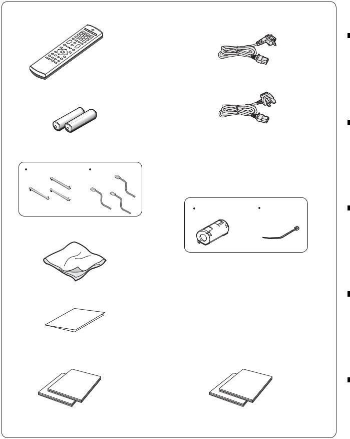
2.1 ACCESSORIES
 Remote control unit (AXD1551)
 Dry cell battery (R6, AA)
 Binder Assy
(AEC1908)
Speed clamp: ×3 |
Bead band: ×3 |
 Cleaning cloth (AED1285)
 Warranty card
 Operating instructions
(PDP-LX5080D/YVIXK5, PDP-LX508D/WYVIXK5) (ARE1473)
(ARC1584)
|
7 |
|
8 |
|
A
 Power cord (2 m)
Only the power cable appropriate for your country or region is supplied:
(ADG1214)
For Europe, except UK and Republic of Ireland
B
(ADG1223)
For UK and Republic of Ireland
C
 Ferrite core (L5321) (ATX1039)
Ferrite core |
Cable tie |
|
(for ferrite core) |
D
 After Image Caution
(PDP-LX5080D/YVIXK5, PDP-LX508D/WYVIXK5: ARM1349) (PDP-LX508D/WYV5: ARM1350)
 Cleaning Caution (ARM1311)
 Caution Card (ARM1310)
E
 Operating instructions (PDP-LX508D/WYV5) (ARE1474)
(ARC1585)
F
|
9 |
|
PDP-LX5080D |
||
|
|
5 |
|
6 |
|
7 |
|
8 |
|
|
|
|
|
|
||||
|
|
|
|
|

|
1 |
|
|
|
|
2 |
|
|
3 |
|
|
4 |
|
|
||
|
2.2 SPECIFICATIONS |
|
|
|
|
|
|
|
|
|
|
|||||
A |
|
|
|
|
|
|
|
|
|
|
|
|
|
|
|
|
|
|
Item |
|
|
|
|
|
50” plasma television, model : PDP-LX5080D/PDP-LX508D |
|
|
||||||
|
|
|
|
|
|
|
|
|
|
|
|
|
|
|||
|
|
Number of pixels |
|
|
|
|
1920 x 1080 pixels |
|
|
|
|
|
|
|||
|
|
|
|
|
|
|
|
|
|
|
|
|
|
|||
|
|
Audio amplifier |
|
|
|
|
17 W + 17 W (1 kHz, 10 %, 6 Ω) |
|
|
|
|
|
|
|||
|
|
|
|
|
|
|
|
|
|
|
|
|
|
|||
|
|
Sound Effect |
|
|
|
|
SRS FOCUS/SRS/SRS TruBass |
|
|
|
|
|
|
|||
|
|
|
|
|
|
|
|
|
|
|
||||||
|
|
Power Requirements |
|
|
|
|
220 V to 240 V AC, 50 Hz/60 Hz, 421 W (0.3 W Standby) |
|
|
|
||||||
|
|
|
|
|
|
|
|
|
|
|
|
|
|
|
||
|
|
Weight |
|
|
|
|
|
38.3 kg (84.4 lbs.) |
|
|
|
|
|
|
||
|
|
|
|
|
|
|
|
|
||||||||
|
|
Colour System |
Analogue |
|
PAL/SECAM/NTSC 3.58/NTSC 4.43/PAL 60 |
|
|
|
||||||||
|
|
|
|
|
|
|
|
|
|
|
|
|
||||
|
|
|
|
Digital |
|
PAL/SECAM |
|
|
|
|
|
|
||||
|
|
|
|
|
|
|
|
|
|
|
|
|||||
B |
|
TV |
Receiving System |
|
B/G, D/K, I, L, L’ |
|
|
|
|
|
|
|||||
|
Function |
|
|
|
|
|
|
|
|
|
|
|
|
|
|
|
|
Tuner |
VHF/UHF |
|
E2–E69 ch, F2–F10 ch, I21–I69 ch, IR A–IR J ch |
|
|
|
|||||||||
|
|
(Analogue) |
|
|
|
|
||||||||||
|
|
|
CATV |
|
Hyper-band, S1–S41 ch |
|
|
|
|
|
|
|||||
|
|
|
|
|
|
|
|
|
|
|
||||||
|
|
|
|
|
|
|
|
|
||||||||
|
|
|
Auto Channel Preset |
|
99 ch, Auto Preset, Auto Label, Auto Sort |
|
|
|
||||||||
|
|
|
|
|
|
|
|
|
|
|
|
|
|
|
||
|
|
|
STEREO |
|
|
|
|
NICAM/A2 |
|
|
|
|
|
|
||
|
|
|
|
|
|
|
|
|
|
|
|
|||||
|
|
TV |
Receiving System |
|
DVB-T(2K/8K COFDM) |
|
|
|
|
|
|
|||||
|
|
Function |
Tuner |
VHF/UHF |
|
VHF Band III (170 MHz to 230 MHz) and UHF Band IV, V (470 MHz to 862 MHz) |
|
|||||||||
|
|
(Digital) |
|
|
||||||||||||
|
|
|
|
|
|
|
|
|
|
|
|
|
|
|
|
|
|
|
Auto Channel Preset |
|
99 ch, Auto Preset, Auto Label, Auto Sort |
|
|
|
|||||||||
|
|
|
|
|
|
|
||||||||||
|
|
|
|
|
|
|
|
|
|
|
|
|
|
|
||
|
|
|
STEREO |
|
|
|
|
MPEG layer I/II, Dolby Digital |
|
|
|
|
|
|
||
|
|
|
|
|
|
|
|
|
||||||||
|
|
Terminals Rear |
INPUT 1 |
|
SCART (AV in, RGB in, TV out), HDMI in *1 |
|
|
|
||||||||
C |
|
|
|
INPUT 2 |
|
SCART (AV in/out, S-VIDEO in, AV link *2), Component Video in, AUDIO in |
|
|
|
|||||||
|
|
|
|
|
|
|
|
|
|
|
|
|
|
|
|
|
|
|
|
INPUT 3 |
|
SCART (AV in/out, S-VIDEO in, RGB in, AV link*2), HDMI in*1 |
|
|
|
||||||||
|
|
|
|
|
|
|
|
|||||||||
|
|
|
|
|
|
|
|
|
|
|
|
|
||||
|
|
|
|
INPUT 4 |
|
HDMI in*1 |
|
|
|
|
|
|
||||
|
|
|
|
CONTROL OUT |
|
1 |
|
|
|
|
|
|
|
|
||
|
|
|
|
|
|
|
|
|
|
|
|
|
||||
|
|
|
|
SPEAKERS |
|
6 Ω to 16 Ω |
|
|
|
|
|
|
||||
|
|
|
|
|
|
|
|
|
|
|
|
|
||||
|
|
|
|
Antenna |
|
75 Ω Din Type for VHF/UHF in |
|
|
|
|
|
|
||||
|
|
|
|
|
|
|
|
|
|
|
|
|
||||
|
|
|
|
PC INPUT |
|
Analogue RGB in, Audio in |
|
|
|
|
|
|
||||
|
|
|
|
|
|
|
|
|
|
|
|
|
||||
|
|
|
|
AUDIO OUT |
|
AUDIO out (Fixed) |
|
|
|
|
|
|
||||
|
|
|
|
|
|
|
|
|
|
|
|
|
||||
|
|
|
|
SUB WOOFER |
|
Variable |
|
|
|
|
|
|
||||
|
|
|
|
|
|
|
|
|
|
|
|
|
||||
|
|
|
|
DIGITAL OUT |
|
Digital audio output (Optical) |
|
|
|
|
|
|
||||
|
|
|
|
|
|
|
|
|
|
|
|
|
||||
D |
|
|
|
COMMON INTERFACE |
|
CA Module |
|
|
|
|
|
|
||||
|
|
|
|
|
|
|
|
|
|
|
|
|
|
|
|
|
|
|
Side |
INPUT 5 |
|
S-VIDEO, AV in |
|
|
|
|
|
|
|||||
|
|
|
|
|
|
|
|
|
|
|||||||
|
|
|
|
|
|
|
|
|
|
|
|
|
||||
|
|
|
|
USB |
|
USB in*3 |
|
|
|
|
|
|
||||
|
|
|
|
|
|
|
|
|
|
|
|
|
||||
|
|
|
|
PHONES |
|
16 Ω to 32 Ω recommended |
|
|
|
|
|
|
||||
|
|
|
|
|
|
|
|
|
|
|
|
|
|
|
|
|
*1 This conforms to HDMI1.3 and HDCP1.1. HDMI (High Definition Multimedia Interface) is a digital interface that handles both video and audio using a single cable. HDCP (High-bandwidth Digital Content Protection) is a technology used to protect copyrighted digital contents that use the Digital Visual Interface (DVI).
*2 Switchable from menu.
*3 This conforms to USB 1.1 and 2.0 specifications.
Design and specifications are subject to change without notice.
E
 Dimensions
|
|
|
1232 |
|
|
|
|
120 |
|
|||
|
|
|
||||||||||
|
|
|||||||||||
|
|
|
|
|
|
|
|
|
|
|
|
|
|
|
|
|
|
|
|
|
|
|
|
|
|
|
|
|
|
|
|
|
|
|
|
|
|
|
|
|
|
|
|
|
|
|
|
|
|
|
|
722
F
Unit: mm
10 |
|
|
PDP-LX5080D |
|
|
|
|
|||
|
1 |
|
2 |
|
|
|
3 |
|
4 |
|
|
|
|
|
|
|
|
||||
|
5 |
|
6 |
|
7 |
|
8 |
2.3 PANEL FACILITIES
 Front Section
Side |
Side |
11 |
|
12 |
7 |
8 |
|
|
9 |
13 |
10 |
|
|
14 |
|
15 |
|
2  3
3
ON STANDBY TIMER |
4 |
|
1 |
5 |
6 |
1 |
button (This button is located on the bottom of the rear |
5 |
Room Light Sensor |
|
panel of the plasma television for the PDP-LX508D/PDP- |
6 |
Remote control sensor |
|
LX5080D. If the button is off, the power will not turn on |
7 |
STANDBY/ON button |
|
even when , 0 to 9 on the remote control unit or |
8 |
INPUT button |
|
STANDBY/ON on the plasma television is pressed. To turn |
9 |
VOLUME +/– buttons |
|
on the power, press . (You can aslo slide up). |
10 |
CHANNEL +/– buttons |
2 |
POWER ON indicator |
11 |
USB port |
3 |
STANDBY indicator |
12 |
PHONES output terminal |
4 |
TIMER indicator |
13 |
INPUT 5 terminal (S-VIDEO) |
|
• The TIMER indicator lights up when one or more DTV |
14 |
INPUT 5 terminal (VIDEO) |
|
programmes are preset for watching or recording. |
15 |
INPUT 5 terminals (AUDIO) |
A
B
C
D
E
F
|
11 |
|
PDP-LX5080D |
||
|
|
5 |
|
6 |
|
7 |
|
8 |
|
|
|
|
|
|
||||
|
|
|
|
|

|
1 |
|
2 |
|
3 |
|
4 |
|
A
 Rear Section
B
C
D
11 12 13 14 15
16 |
17 |
18 |
19 |
20 |
4 |
3 |
1 |
2 |
5 6 7 8 9 10
|
1 |
button |
11 |
INPUT 1 terminal (SCART) |
|
|
|||||
|
2 |
AC IN terminal |
12 |
INPUT 2 terminal (SCART) |
|
E |
3 |
RS-232C terminal (used for factory setup) |
13 |
INPUT 3 terminal (SCART) |
|
4 |
CONTROL OUT terminal (supports SR+) |
14 |
INPUT 2 terminals (Audio) |
||
|
|||||
|
5 |
INPUT 1 terminal (HDMI) |
15 |
INPUT 2 terminals (COMPONENT VIDEO: Y, PB, PR) |
|
|
6 |
INPUT 3 terminal (HDMI) |
16 |
AUDIO OUT terminals |
|
|
7 |
INPUT 4 terminal (HDMI) |
17 |
SUBWOOFER output terminal |
|
|
8 |
PC INPUT terminal (Analogue RGB) |
18 |
PC INPUT terminal (Audio) |
|
|
9 |
COMMON INTERFACE slot |
19 |
DIGITAL OUT terminal (OPTICAL) |
|
|
|||||
|
|
• For a CA Module with a smart card |
20 |
SPEAKERS terminals (right/left) |
10ANT (Antenna) input terminal
•Power can be supplied through this terminal
F
12 |
|
|
PDP-LX5080D |
|
|
|
|
|||
|
1 |
|
2 |
|
|
|
3 |
|
4 |
|
|
|
|
|
|
|
|
||||

|
5 |
|
6 |
 Remote Control Unit
This section describes the functions of the buttons available when the mode switch has been set to TV.
1
2 |
1 |
2 |
3 |
|
4 |
|
|
|
INPUT |
|
|
|
|
|
1 |
|
2 |
|
3 |
|
3 |
4 |
|
5 |
|
6 |
|
|
7 |
|
8 |
|
9 |
|
4 |
|
|
0 |
|
INFO |
19 |
PC |
|
|
|
|||
5 |
INPUT 5 |
|
|
|
|
20 |
|
|
|
|
|
||
6 |
|
TV/DTV |
|
|
21 |
|
7 |
P |
|
|
|
|
22 |
8 |
SELECT |
|
DVD/ |
|
SOURCE |
23 |
9 |
|
TV STB DVR VCR |
|
|
||
|
|
|
|
|
|
|
10 |
RETURN |
|
|
HOME MENU |
|
|
|
|
|
|
|
||
|
|
|
|
MENU |
24 |
|
11 |
|
|
|
|
||
|
ENTER |
|
|
|||
12 |
|
|
|
|
||
EXIT |
|
|
|
EPG |
25 |
|
13 |
|
|
DVD TOP MENU / GUIDE |
|||
14 |
|
|
|
|
|
|
15 |
|
|
|
|
|
26 |
16 |
HDMI |
|
|
|
|
27 |
17 |
CONTROL |
|
|
|
|
|
|
NAVI |
DVD |
|
HDD |
|
|
|
|
DISC |
|
28 |
||
18 |
|
|
|
|
|
|
|
|
|
|
|
|
|
29
1  : Turns on the power to the plasma television or places it into the standby mode.
2 INPUT: Selects an input source of the plasma television. (“INPUT 1”, “INPUT 2”, “INPUT 3”, “INPUT 4”)
3 0 to 9: TV/External input mode: Selects a channel. Teletext mode: Selects a page.
Turns the power on when the STANDBY indicator lights red.
4PC: Selects the PC terminal as an input source.
5INPUT 5: Selects INPUT 5 as the input source of the plasma
television.
|
7 |
|
8 |
6  :Switches the screen mode among 2-screen, picture-in- picture, and single-screen.
7 P+/P–: TV/External input mode: Selects a channel.
 / :Teletext mode: Selects a page.
8TV/DTV: Switches between the TV and DTV input modes.
9SELECT: Switches the selection among TV, STB, DVD/DVR,
and VCR, so that you can control other connected equipment, using the supplied remote control unit.
10 TV, STB, DVD/DVR, VCR: These indicators show the current selection and status when you control other connected equipment, using the supplied remote control unit.
11 RETURN: Restores the previous menu screen.
12 /
/ /
/ /
/ :Selects a desired item on the setting screen.
ENTER: Executes a command.
13EXIT: Returns to the normal screen in one step.
14Colour (RED/GREEN/YELLOW/BLUE):
Teletext mode: Selects a page.
15  : Jumps to Teletext subtitle page.
Turns subtitle on and off in DTV input mode depending on the broadcast.
16 : Displays hidden characters.
17HDMI CONTROL: Displays the HDMI Control menu.
18: Sets the sound multiplex mode.
19
 INFO: Displays the channel information.
Displays the banner information in DTV input mode.
20  : Moves the location of the small screen when in the picture-in-picture mode.
21  : Switches between the two screens when in the 2-screen or picture-in-picture mode.
22 |
+/ |
–: Sets the volume. |
23 : Mutes the sound.
24HOME MENU: Displays the HOME MENU screen.
25EPG: Displays the Electronic Programme Guide in DTV input
mode.
26  : Selects the Teletext mode (all TV image, all TEXT image, TV/TEXT image).
27  : Displays an Index page for the CEEFAX/FLOF format. Displays a TOP Over View page for the TOP format.
28: Selects the screen size.
29 : TV/External input mode: Freezes a frame from a moving
image. Press again to cancel the function.
 : Teletext mode: Stops updating Teletext pages. Press again to release the hold mode.
 Note
Note
•When using the remote control unit, point it at the plasma television.
A
B
C
D
E
F
|
13 |
|
PDP-LX5080D |
||
|
|
5 |
|
6 |
|
7 |
|
8 |
|
|
|
|
|
|
||||
|
|
|
|
|

|
1 |
|
2 |
|
3 |
|
4 |
|
3. BASIC ITEMS FOR SERVICE
3.1 CHECK POINTS AFTER SERVICING
A
Items to be checked after repair (PDP)
To ensure the quality of the product after repair, check the recommended items shown below:
|
|
No. |
Procedures |
Item to be checked |
|
|
1 |
Check if all the symptoms pointed out by the customer have been |
The symptoms in question must not be reproduced. |
|
||||
|
|
|
addressed. |
|
|
|
|
|
|
|
|
2 |
Connect the peripheral equipment. |
Connect all external peripheral equipment as originally connected |
|
|
and check if the connections are correct. |
||
|
|
|
|
|
|
|
|
|
|
|
|
3 |
Check the video and audio. |
Tune in to the stations that the customer would normally receive |
|
|
and check if video and audio are normal. |
||
|
|
|
|
|
B |
|
4 |
Check the buttons and controls. |
Use the buttons and controls on the remote control unit and main |
|
|
unit and check if they operate properly. |
||
|
|
|
|
|
|
|
|
|
|
|
|
5 |
Check the cabinet. |
Check for any scratches or dirt that have been made or attached |
|
|
on the cabinet after receiving the product for repair. |
||
|
|
|
|
|
|
|
|
|
|
|
|
|
|
|
|
|
|
|
|
See the table below for the items to be checked regarding video and audio:
|
|
Item to be checked regarding video |
Item to be checked regarding audio |
|
|
Block noise |
Distortion |
|
|
|
|
|
|
Horizontal noise |
Noise |
C |
|
|
|
|
Dot noise |
Volume too low |
|
|
|
||
|
|
|
|
|
|
Disturbed image (video jumpiness) |
Volume too high |
|
|
|
|
|
|
Too dark |
Volume fluctuating |
|
|
|
|
|
|
Too bright |
Sound interrupted |
|
|
|
|
|
|
Mottled color |
|
|
|
||
|
|
|
|
D
E
F
14 |
|
|
PDP-LX5080D |
|
|
|
|
|||
|
1 |
|
2 |
|
|
|
3 |
|
4 |
|
|
|
|
|
|
|
|
||||

|
5 |
|
6 |
|
7 |
|
8 |
3.2 QUICK REFERENCE
Quick Reference upon Service Visit 1
Notes, PD/SD diagnosis, and methods for various settings
Notes when visiting for service
1.Notes when disassembling/reassembling
1Rear case
When reassembling the rear case, the screws must be tightened in a specific order. Be careful not to tighten them in the wrong order forcibly. For details, see "Rear Case" in "7. DISASSEMBLY".
2Attaching screws for the HDMI connector
When attaching the HDMI connector after replacing the Main Assy, secure the HDMI connector manually with a screwdriver, but not with an electric screwdriver. If you tighten the screws too tightly with an electric screwdriver, the screw heads may be damaged, in which case the screws cannot be untightened/tightened any more.
2.On parts replacement
1How to discharge before replacing the Assys
A charge of significant voltage remains in the Plasma Panel even after the power is turned off. Safely discharge the panel before replacement of parts, in either manner indicated below:
A:Let the panel sit at least for 3 minutes after the power is turned off.
B:Turn the Large Signal System off before the power is turned off then, after 1 minute, turn the power off.
For details, see "5.6.1 PANEL DRIVE-POWER ON/OFF FUNCTION".
2 On the settings after replacement of the Assys
Some boards need settings made after replacement of the Assys. For details, see "8. EACH SETTING AND ADJUSTMENT".
3.On various settings
1Setting in Factory mode
After a Mask indication into the panel is performed, be sure to set the Mask setting to "OFF" then exit Factory mode.
PD/SD
|
|
No. of LEDs |
|
|
Item |
flashing |
|
|
|
Red |
Blue |
section |
SQ_LSI |
|
Blue 1 |
Communication with the module IIC |
|
Blue 2 |
|
Panel |
DIGITAL-RST2 |
|
Blue 3 |
Panel high temperature |
|
Blue 4 |
|
|
Audio/ Short-circuit SP terminal |
|
Blue 5 |
|
Communication with the Module UCOM |
|
Blue 6 |
section |
Main 3-wire serial communication |
|
Blue 7 |
Main IIC communication |
|
Blue 8 |
|
Communication with the Main UCOM |
|
Blue 9 |
|
MTB |
|
||
FAN |
|
Blue 10 |
|
|
Unit high temperature |
|
Blue 11 |
|
Digital Tuner communication |
|
Blue 12 |
|
MTB-RST2/RST4 |
|
Blue 13 |
|
Main EEPROM |
|
Blue 15 |
POWER |
Red 2 |
|
|
SCAN |
Red 3 |
|
|
SCN-5V |
Red 4 |
|
|
Y-DRIVE |
Red 5 |
|
|
Y-DCDC |
Red 6 |
|
|
Y-SUS |
Red 7 |
|
|
ADRS |
Red 8 |
|
|
X-DRIVE |
Red 9 |
|
|
X-DCDC |
Red 10 |
|
|
X-SUS |
Red 11 |
|
|
DIG-DCDC |
Red 12 |
|
|
UNKNOWN |
Red 15 |
|
|
LED Display Information
Rewriting software
PD (2-15)
SD (1-15)
No backup
This indication does not display all LED patterns.
For details, please refer to 5.1.1 LED DISPLAY INFORMATION.
A
B
C
How to locate several items on the Factory menu
{} : Item on the Factory menu
[ ] : Key on the remote control unit
"" : Screen indication
1.Confirmation of accumulated power-on time and power-on count
Select {INFORMATION} then {HOUR METER}. (After entering Factory mode, press [ ] five times.)
2.Confirmation of the Power-down and Shutdown histories
1 Panel system
PD: Select {PANEL FACTORY} then {POWER DOWN}.
(After entering Factory mode, press [MUTING] once, press [ENTER/SET], then press [ ] three times.)
SD: Select {PANEL FACTORY} then {SHUT DOWN}.
(After entering Factory mode, press [MUTING] once, press [ENTER/SET], then press [ ] four times.)
2 MTB section
Select {INFORMATION} then {MAIN NG}.
(After entering Factory mode, press [ ] three times.)
3.How to display the Mask indication
1 Mask indication in the panel side
1. Select {PANEL FACTORY} then {RASTER MASK SETUP}.
(After entering Factory mode, press [MUTING] once, press [ENTER/SET], then press [ ] 8 times.)
2. Press [ENTER/SET], then select a Mask indication, using [ ] or [ ].
Adjustments and Settings after replacement of the Assys (Procedures in Factory mode)
1.Digital Video Assy: Transfer of backup data
Select {PANEL FACTORY}, {ETC}, then {BACKUP DATA}. (After entering Factory mode, press [MUTING] once, press [ENTER/SET], press [ ] seven times, then press [ENTER/SET].)
Select {TRANSFER}, using [ ], then hold [ENTER/SET] pressed for at least 5 seconds.
After transfer of backup data is completed, {ETC} is automatically selected, and the LED on the front panel returns to normal lighting.
2.MAIN Assy: Execution of FINAL SETUP.
Select {INITIALIZE} then {FINAL SETUP}, then press [ENTER/SET]. (After entering Factory mode, press [MUTING] three times, then press [ ] four times.)
Select "YES", using [ ]. Then hold [ENTER/SET] pressed for at least 5 seconds.
After "FINAL SETUP IS COMPLETE" is displayed on the screen, turn the POWER switch of the main unit off.
3.POWER SUPPLY Unit: Clearance of the accumulated power-on count and maximum temperature value
Select {PANEL FACTORY}, {ETC}, then {P COUNT INFO}. (After entering Factory mode, press [MUTING] once, press [ENTER/SET], press [ ] seven times, press [ENTER/SET], then press [ ] six times.)
Press [ ] to select "CLEAR". Hold [ENTER/SET] pressed for at least 5 seconds. After clearance is completed, "ETC" is automatically selected. Clear the maximum temperature value (MAX TEMP) in the same manner.
4.Other Assys: Clearance of the maximum temperature value
Select {PANEL FACTORY}, {ETC}, then {MAX TEMP}. (After entering Factory mode, press [MUTING] once, press [ENTER/SET], press [ ] seven times, press [ENTER/SET], then press [ ] seven times.)
Press [ ] to select "CLEAR". Hold [ENTER/SET] pressed for at least 5 seconds. After clearance is completed, "ETC" is automatically selected.
D
E
F
|
15 |
|
PDP-LX5080D |
||
|
|
5 |
|
6 |
|
7 |
|
8 |
|
|
|
|
|
|
||||
|
|
|
|
|
|
1 |
|
2 |
|
3 |
|
4 |
|
Quick Reference upon Service Visit 2
A
Mode transition and structure of layers in Service Factory mode
|
Mode transition in Service Factory mode |
Structure of Layers in Service Factory Mode |
||||||||||
|
|
Up |
• To shift to another mode, press [MUTING]. |
|
|
|||||||
|
|
|
|
|
INFORMATION mode |
|
||||||
|
|
|
|
|
• To shift to another item in a specific mode, |
|
||||||
|
|
|
|
|
1. VERSION (1) |
The software versions for each microcomputer |
||||||
|
|
|
|
|
press [ ] or [ ]. |
|||||||
|
|
|
|
|
2. VERSION (2) |
The Flash memory versions for each device |
||||||
|
|
|
|
|
• To shift to the next nested layer below for an |
3. MAIN NG |
The shutdown message ID/event times |
|||||
|
|
|
|
|
item with a "(+)" indication, press [ENTER/SET]. |
|||||||
|
|
|
|
|
|
(Going Clear mode by [ENTER/SET] key) |
||||||
|
|
|
|
|
To return to the next nested layer above, |
3-1. CLEAR |
Select Yes by [ ] key, pressing and hold [ENTER/SET] key |
|||||
|
|
Down |
also press [ENTER/SET]. |
4. TEMPERATURE |
The temperature/FAN rotating status/Room light sensor |
|||||||
|
|
|
|
|
|
|
|
5. HOUR METER |
The HOUR METER/P-COUNT information |
|||
|
|
|
|
|
|
|
|
|
|
|
||
|
|
INFORMATION mode |
|
|
INITIALIZE mode |
|
6. HDMI SIGNAL INFO 1 |
The information of HDMI information files |
||||
|
|
1. VERSION (1) |
|
|
1. SIDE MASK LEVEL |
|
7. HDMI SIGNAL INFO 2 |
The information of HDMI information files |
||||
|
|
|
|
|
||||||||
B |
|
2. VERSION (2) |
|
|
2. FINAL SETUP |
|
8. VDEC SIGNAL INFO 1 |
The signal information of VDEC |
||||
|
3. MAIN NG |
|
|
3. Wide XGA AUTO |
|
9. VDEC SIGNAL INFO 2 |
The signal information of VDEC |
|||||
|
|
|
|
|
||||||||
|
|
4. TEMPERATURE |
|
|
|
|
|
|
|
|
||
|
|
5. HOUR METER |
|
|
|
|
|
|
PANEL FACTORY mode |
Refer to [PANEL FACTORY MODE] |
||
|
|
6. HDMI SIGNAL INFO1 |
|
|
|
|
|
|
|
|
||
|
|
7. HDMI SIGNAL INFO2 |
|
|
|
|
|
|
OPTION mode |
|
||
|
|
8. VDEC SIGNAL INFO1 |
|
|
|
|
|
|
|
|||
|
|
|
|
|
|
|
|
1. EDID WRITE MODE |
For factory use |
|||
|
|
9. VDEC SIGNAL INFO2 |
|
|
|
|
|
|
||||
|
|
|
|
|
|
|
|
2. CH PRESET |
For production line use |
|||
|
|
|
|
|
|
|
|
|
|
|
||
|
|
|
|
|
|
|
|
|
|
|
3. SYNC DET |
For technical analysis |
|
|
|
|
|
|
|
|
|
|
|
||
|
|
|
|
|
|
|
|
|
|
|
INITIALIZE mode |
|
|
|
|
|
|
|
|
|
|
|
|
|
|
|
|
|
|
|
|
|
|
|
|
|
1. SIDE MASK LEVEL |
For factory use |
|
|
|
|
|
|
|
|
|
|
|
1-1. SIDE MASK LEVEL |
|
|
|
PANEL FACTORY mode |
|
|
OPTION mode |
|
||||||
|
|
|
|
2. FINAL SETUP |
Set to Factory default settings (it should perform after |
|||||||
|
|
1. PANEL INFORMATION |
|
|
1. EDID WRITE MODE |
|||||||
|
|
|
|
2-1. DATA RESET |
replacing a MAIN Assy) |
|||||||
|
|
2. PANEL WORKS |
|
|
2. CH PRESET |
|||||||
|
|
|
|
3. Wide XGA AUTO |
For technical analysis |
|||||||
|
|
3. POWER DOWN |
|
|
3. SYNC DET |
|||||||
|
|
|
|
|
|
|||||||
|
|
4. SHUT DOWN |
|
|
|
|
|
|
|
|
||
C5. PANEL-1 ADJ
6.PANEL-2 ADJ
7.PANEL FUNCTION
8.ETC.
9.RASTER MASK SETUP
10.PATTEN MASK SETUP
11.COMBI MASK SETUP
|
|
|
|
|
|
|
|
|
|
Structure of Layers in Panel Factory Mode 1 |
|
|
|
1. PANEL INFORMATION |
Version indication of the panel |
|
|
2. PANEL WORKS |
Indications of the accumulated power-on time, pulse-meter |
|
|
|
count, and power-on count of the panel |
|
|
3. POWER DOWN |
Indication of the Power-down history |
D |
|
4. SHUT DOWN |
Indication of the Shutdown history |
|
|
5. PANEL-1 ADJ (+) |
|
|
|
1. VOL SUS |
|
|
|
2. VOL OFFSET |
Settings required after replacement of the panel |
|
|
• • • • • |
|
|
|
|
|
|
|
8. VOL YNOFS4 |
|
|
|
9. RESET1ST_KSB |
|
|
|
10. RESET2ND_KSB |
Modification not required because these items |
|
|
• • • • • |
are basically for factory presetting |
|
|
|
|
|
|
23. YSTL_FMR_HZ |
|
|
|
24. SUS FREQ |
For AM noise prevention (Depending on the mode, |
|
|
|
brightness of the screen changes.) |
|
|
|
For confirmation of the result of the setting change, |
|
|
|
the unit must be turned off then back on again. |
|
|
6. PANEL-2 ADJ (+) |
|
|
|
1. R-HIGH |
|
E |
|
2. G-HIGH |
|
|
|
3 .B-HIGH |
Parameters for the WB adjustment of the panel, which are |
|
|
4. R-LOW |
required during adjustment after panel replacement |
|
|
5. G-LOW |
|
|
|
6. B-LOW |
|
|
|
7. ABL |
Setting of the power consumption. A setting table is |
|
|
|
available for each vertical signal. |
|
|
To "Structure of Layers in Panel Factory Mode 2" |
|
|
|
||
|
|
|
|
F
Structure of Layers in Panel Factory Mode 2
7. PANEL FUNCTION (+) |
|
1. R-LEVEL |
|
2. G-LEVEL |
|
3. B-LEVEL |
|
4. ADDRESS L1 |
Items for use by engineers |
5. ADDRESS L2 |
|
• • • • • |
|
11. ADDRESS U4 |
|
12. STK MODE |
|
8. ETC (+) |
|
1. BACKUP DATA |
For transferring backup data (after replacement of |
|
the DIGITAL Assy) |
2. DIGITAL EEPROM |
To clear data of the digital video |
3. PD INFO. |
|
4. SD INFO. |
For clearance of data for the corresponding items. |
5. HR-MTR INFO. |
The clearing method is the same: Select "CLEAR", |
6. PM/B1-B5 |
using [ ], then hold [ENTER/SET] pressed for at |
7. P COUNT INFO. |
least 5 seconds. After clearance is completed, {ETC} |
8. MAX TEMP. |
is automatically selected. |
9.RASTER MASK SETUP (+)
1.MASK OFF
2. RST MASK 01 |
For use while Raster Mask (full mask) is displayed. |
• • • • • |
Use [ ] or [ ] to select the type of mask. |
26.RST MASK 25
10.PATTEN MASK SETUP (+)
1.MASK OFF
2. PTN MASK 01 |
For use while Pattern Mask is displayed. Use [ ] or |
• • • • • |
[ ] to select the type of mask. |
50.PTN MASK 49
11.COMBI MASK SETUP (+)
1.MASK OFF
2. CMB MASK 01 |
For use while Combination Mask is displayed. |
• • • • • |
Use [ ] or [ ] to select the type of mask. |
18. CMB MASK 17 |
|
16 |
|
|
PDP-LX5080D |
|
|
|
|
|||
|
1 |
|
2 |
|
|
|
3 |
|
4 |
|
|
|
|
|
|
|
|
||||

|
5 |
|
6 |
|
7 |
|
8 |
|
3.3 PCB LOCATION
A
Note:
The wiring shown in the photo is different from the actual wiring, because the product in the photo is a prototype. Upon servicing, be sure to restore the original wiring of the unit after repair work.
PANEL SENSOR |
FHD FAN CONNECT |
Assy |
Assy |
|
|
|
|
50F ADDRESS L |
|
|
50F ADDRESS L |
|
|
50F ADDRESS L |
||||||||||
|
|
|
|
|
Assy |
|
|
|
Assy |
|
|
|
|
|
|
Assy |
||||
|
SCAN A Assy |
|
|
|
|
|
|
|
|
|
|
|
|
|
|
|
|
|
|
|
|
|
|
|
|
|
|
|
|
|
|
|
|
|
|
|
|
|
|
|
|
|
|
|
|
|
|
|
|
|
|
|
|
|
|
|
|
|
|
|
|
|
|
|
|
|
|
|
|
|
|
|
|
|
|
|
|
|
|
|
|
|
|
|
50F |
|
|
|
|
|
|
|
|
|
|
|
|
|
|
|
|
|
|
|
|
|
|
|
|
|
|
|
|
|
POWER SUPPLY |
|
|
|
|
|
|
|
|||
|
|
|
|
|
|
|
|
|
|
|
|
|
|
|
|
|
|
|||
|
B |
|
|
|
|
|
|
|
|
|
|
Unit |
|
|
|
|
|
|
|
|
|
SCAN Assy |
|
|
50F Y DRIVE |
|
|
|
|
|
|
|
|
|
|
|
|
|
|||
|
|
|
|
|
|
|
|
|
|
|
|
|
|
|
|
|||||
|
|
|
|
|
|
|
|
|
|
|
|
|
|
|
|
|
||||
Assy |
50F |
|
|
Assy |
|
|
|
|
|
|
|
|
|
|
|
|
|
|||
|
|
|
|
|
|
|
|
|
|
|
|
|
|
|
|
|
|
|
||
KEY |
|
|
|
|
|
|
|
|
|
|
|
|
|
|
|
|
|
|
|
|
C |
|
|
|
|
|
|
|
|
|
|
|
|
|
|
|
|
|
|
|
|
SIDE |
SCAN Assy |
|
|
|
|
|
|
|
|
|
|
|
|
|
|
|
|
|
|
|
|
|
|
|
|
|
|
|
|
|
|
|
|
|
|
MAIN |
|
|
|||
|
|
|
|
|
|
|
|
|
|
|
|
|
|
|
|
|
|
|
||
|
50F |
|
|
|
|
|
|
|
|
|
|
|
|
|
|
|
Assy |
|
|
|
|
|
|
|
|
|
|
|
|
|
|
|
|
|
|
|
|
|
|||
|
|
|
|
|
|
|
|
|
|
|
|
|
|
|
|
|
|
|
|
|
|
|
|
|
|
|
|
|
|
|
|
|
|
|
|
|
|
|
|
|
|
|
D |
|
|
|
|
|
|
|
|
|
|
|
|
|
|
|
|
|
|
|
|
SCAN Assy |
|
|
|
|
|
|
|
|
|
|
|
|
|
|
|
|
|
|
|
|
|
|
|
|
|
|
|
TANSHI Assy |
|
|
|
|
|
|
|
|
||||
|
50F |
|
|
|
|
|
|
|
|
|
|
|
|
|
|
|
||||
|
|
|
|
|
|
|
|
|
|
|
|
|
|
|
|
|
|
|
|
|
|
|
|
|
|
|
|
|
|
|
|
|
|
|
|
|
|
|
|
|
|
|
|
|
|
|
|
|
|
|
|
|
|
|
|
|
|
|
|
|
|
|
|
|
|
|
50F ADDRESS S |
50F ADDRESS L |
232C |
|
50F ADDRESS L |
||||||||||||
|
|
|
|
Assy |
Assy |
Assy |
|
|
|
Assy |
||||||||||
|
|
|
|
|
|
|
|
|
|
|
|
|
50F DIGITAL |
|||||||
|
|
|
|
|
|
|
|
|
|
|
|
|
||||||||
|
|
|
|
|
|
|
|
|
|
|
|
|
Assy |
|
|
|
|
|
|
|
|
|
|
|
FHD RLS |
|
|
|
|
|
|
|
|
|
|
|
|
|
|
|
|
FHD IR Assy |
Assy |
|
|
|
|
|
|
|
|
|
|
|
|
|
|
|
||||
|
|
|
|
|
|
|
|
|
|
|
|
|
|
|
|
|
||||
|
|
Bottom view |
|
|
|
|
|
|
|
Rear view |
||||||||||
|
|
|
|
|
|
|
|
|
|
|
|
|
||||||||
50F ADDRESS S
Assy
50F X DRIVE
Assy
|
|
|
|
SIDE IO Assy |
|
|
|
|
|
|
|
|
|
SW |
|
|
|
|
POWER Assy |
|
|
|
|
|
|
|
|
|
FHD |
50F ADDRESS L |
|
|||
|
|
|||
Assy |
|
|
||
50FHD LED Assy
 Front view
Mark No. Description |
|
Part No. |
Mark No. Description |
Part No. |
|||
|
|
|
|
|
|
|
|
LIST OF ASSEMBLIES
B
C
D
NSP |
50F ADDRESS L ASSY |
AWW1310 |
MAIN ASSY |
AWV2464 |
||
NSP |
50F ADDRESS S ASSY |
AWW1311 |
|
|
||
|
|
|
|
|
SIDE IO ASSY |
AWW1253 |
NSP |
50F SCAN A ASSY |
AWW1312 |
SIDE KEY ASSY |
AWW1286 |
||
|
|
|
IC2801 - IC2804 |
AN16174A |
TANSHI ASSY |
AWW1331 |
|
|
|
||||
NSP |
50F SCAN B ASSY |
AWW1313 |
FHD IR ASSY |
AWW1289 |
||
|
|
|
IC2901 - IC2904 |
AN16174A |
FHD FAN CONNECT ASSY |
AWW1290 |
|
|
|
||||
NSP |
50F SCAN C ASSY |
AWW1314 |
|
|
||
|
|
|
IC3001 - IC3004 |
AN16174A |
50FHD LED ASSY |
AWW1291 |
|
|
|
||||
NSP |
50F SCAN D ASSY |
AWW1315 |
FHD RLS ASSY |
AWW1292 |
||
|
|
|
IC3101 - IC3104 |
AN16174A |
FHD POWER SW ASSY |
AWW1293 |
|
|
|
||||
|
|
|
|
|
232C ASSY |
AWW1254 |
|
50F X DRIVE ASSY |
AWV2510 |
|
|
||
|
50F Y DRIVE ASSY |
AWV2511 |
> POWER SUPPLY UNIT |
AXY1168 |
||
|
PANEL SENSOR ASSY |
AWW1309 |
|
|
||
|
50F DIGITAL ASSY |
AWW1316 |
PDP SERVICE ASSY 508F |
AWU1272 |
||
|
|
|
|
|
(for PDP-LX5080D/YVIXK5) |
|
|
|
|
|
|
PDP SERVICE ASSY 508F-E |
AWU1273 |
|
|
|
|
|
(for PDP-LX508D/WYVIXK5, /WYV5) |
|
|
17 |
|
PDP-LX5080D |
||
|
|
5 |
|
6 |
|
7 |
|
8 |
|
|
|
|
||||
|
|
|
|
E
F

|
1 |
|
2 |
|
3 |
|
4 |
|
3.4 JIGS LIST
Name |
Jig No. |
Remarks |
A
B
C
3.5 CLEANING
|
|
|
|
|
|
|
|
|
|
D |
|
Name |
Part No. |
Remarks |
|
|
Cleaning liquid |
GEM1004 |
Used to fan cleaning. |
|
|
|
|
|
|
|
Cleaning paper |
GED-008 |
Refer to “10.4 CHASSIS SECTION (1/2)”. |
|
|
|
||
|
|
|
|
|
|
|
|
|
|
E
F
18 |
|
|
PDP-LX5080D |
|
|
|
|
|||
|
1 |
|
2 |
|
|
|
3 |
|
4 |
|
|
|
|
|
|
|
|
||||

|
5 |
|
6 |
|
7 |
|
8 |
|
A
B
C
D
E
F
|
19 |
|
PDP-LX5080D |
||
|
|
5 |
|
6 |
|
7 |
|
8 |
|
|
|
|
|
|
||||
|
|
|
|
|

|
1 |
|
2 |
|
3 |
|
4 |
|
4. BLOCK DIAGRAM
4.1 OVERALL WIRING DIAGRAM (1/2)
A
B
C
D
E
F
20 |
|
|
PDP-LX5080D |
|
|
|
|
|||
|
1 |
|
2 |
|
|
|
3 |
|
4 |
|
|
|
|
|
|
|
|
||||
|
5 |
|
6 |
|
7 |
|
8 |
 When ordering service parts, be sure to refer to "EXPLODED VIEWS and PARTS LIST" or "PCB PARTS LIST".
 The
The  mark found on some component parts indicates the importance of the safety factor of the part. Therefore, when replacing, be sure to use parts of identical designation.
|
21 |
|
PDP-LX5080D |
||
|
|
5 |
|
6 |
|
7 |
|
8 |
|
|
|
|
||||
|
|
|
|
A
B
C
D
E
F

|
1 |
|
2 |
|
3 |
|
4 |
|
4.2 OVERALL WIRING DIAGRAM (2/2)
A
B
C
D
E
F
22 |
|
|
PDP-LX5080D |
|
|
|
|
|||
|
1 |
|
2 |
|
|
|
3 |
|
4 |
|
|
|
|
|
|
|
|
||||

|
5 |
|
6 |
|
7 |
|
8 |
|
A
B
C
D
E
F
|
23 |
|
PDP-LX5080D |
||
|
|
5 |
|
6 |
|
7 |
|
8 |
|
|
|
|
|
|
||||
|
|
|
|
|

|
|
|
|
1 |
|
|
|
|
|
|
|
|
|
2 |
|
|
|
|
|
|
|
|
|
|
|
3 |
|
|
|
|
4 |
|
|
|
|
|
|
4.3 OVERALL BLOCK DIAGRAM (1/2) |
|
|
|
|
|
|
|
|
|
|
|
|
|
|
|
|
|||||||||||||||||||
|
50F ADDRESS L ASSY |
|
|
|
|
|
|
50F ADDRESS L ASSY |
|
|
|
|
|
|
|
|
|
|
|
|
|
|
|
|
|
|||||||||||
A |
DRIVER IC |
|
DRIVER IC |
|
|
|
DRIVER IC |
DRIVER IC |
|
DRIVER IC |
|
DRIVER IC |
|
|
|
DRIVER IC |
|
DRIVER IC |
|
|
|
|
|
|
|
|
|
|||||||||
IC1651 |
|
IC1661 |
|
|
|
IC1671 |
IC1681 |
|
IC1651 |
|
IC1661 |
|
|
|
IC1671 |
|
|
IC1681 |
|
|
|
|
|
|
|
|
|
|||||||||
|
|
|
|
|
|
|
|
|
|
|
|
|
|
|
|
|
|
|
|
|
|
|
|
|
|
|
|
|
|
|
|
|
|
|
SECONDARY |
|
|
|
|
|
|
|
|
|
|
|
|
|
|
|
|
|
|
|
|
|
|
|
|
|
|
|
|
|
|
|
P1 |
|
+16.5V |
|
|
|
|
|
|
|
|
|
|
|
|
|
|
|
|
|
|
|
|
|
|
|
|
|
|
|
|
|
|
|
|
|
|
|
|
+6.5V |
|
|
|
|
|
|
|
|
|
|
|
|
|
|
|
|
|
|
|
|
|
|
|
|
|
|
|
|
|
|
|
|
|
|
|
|
VSUS |
|
|
|
|
|
|
CLK / LE / HBLK / LBLK |
|
|
|
|
|
|
|
|
|
|
CLK / LE / HBLK / LBLK |
|
|
|
|
|
|
|
|
|
|
|
|
|
|
|
|
|
|
|
||||
|
|
R/G/B |
|
|
|
|
|
|
|
|
|
|
|
|
R/G/B |
|
|
|
|
|
|
|
|
|
|
|
|
|
|
P2 |
|
+16.5V |
|
|
|
|
|
|
|
|
|
|
|
|
|
|
|
|
|
|
|
|
|
|
|
|
|
|
|
|
|
|
|
|
|
|
|
+6.5V |
|
|
|
||
|
|
|
|
|
|
|
|
|
|
|
|
|
|
|
|
|
|
|
|
|
|
|
|
|
|
|
|
|
|
|
|
|
|
|
||
|
VADR1 |
VDDLS1 |
|
VADR2 |
VDDLS2 |
|
VADR3 |
VDDLS3 |
VADR4 |
VDDLS4 |
VADR1 |
VDDLS1 |
VADR2 |
VDDLS2 |
|
|
VADR3 |
VDDLS3 |
|
VADR4 |
VDDLS4 |
|
|
|
|
|
|
|
|
|
||||||
|
RESONANCE |
|
RESONANCE |
|
|
RESONANCE |
RESONANCE |
|
RESONANCE |
|
RESONANCE |
|
|
RESONANCE |
|
RESONANCE |
|
|
P7 |
|
+12V |
|
|
|
|
|||||||||||
|
|
|
|
|
|
|
|
|
|
|
|
+5.1V |
|
|
|
|||||||||||||||||||||
|
BLOCK |
|
BLOCK |
|
|
|
BLOCK |
|
BLOCK |
|
BLOCK |
|
BLOCK |
|
|
|
BLOCK |
|
BLOCK |
|
|
|
|
|
|
|
||||||||||
|
|
|
|
|
|
|
|
|
|
|
|
|
|
|
|
|
|
|
|
|
|
|
|
|
|
|
|
|
|
|
|
+60V |
|
|
|
|
|
|
|
|
|
|
|
|
|
|
|
|
|
|
|
|
|
|
|
|
|
|
|
|
|
|
|
|
|
|
|
|
+12V |
|
|
|
|
|
|
|
|
|
|
|
|
|
|
|
|
|
|
|
|
|
|
|
|
|
|
|
|
|
|
|
|
|
|
P6 |
|
+5.1V |
|
|
|
|
|
|
|
|
|
|
|
IC1601 |
|
|
|
|
|
|
|
|
|
|
|
IC1601 |
|
|
|
|
|
|
|
|
P5 |
|
+16.5V |
|
|
|
|||
|
|
|
|
|
|
|
LVDS |
|
|
|
|
|
|
|
|
|
|
|
LVDS |
|
|
|
|
|
|
|
|
|
|
|
|
|||||
|
|
V+60V |
+8V |
|
|
|
|
|
|
|
|
|
V+60V +8V |
|
|
|
|
|
|
|
|
|
|
|
|
|
|
|
|
|
||||||
|
|
V+3.3V |
|
|
|
|
|
|
|
|
V+3.3V |
|
|
|
|
|
|
|
|
|
|
|
|
|
|
|
|
|
||||||||
|
|
|
Receiver |
|
|
|
|
|
|
|
Receiver |
|
|
|
|
|
|
|
|
|
|
+5.1V |
|
|
|
|||||||||||
|
|
|
V |
|
|
|
|
|
|
|
|
|
|
|
|
V |
|
|
|
|
|
|
|
|
|
|
|
|
|
|
|
DRF_SW_B |
|
|
|
|
|
|
|
|
|
|
|
|
AN/P BN/P |
|
|
|
|
|
|
|
|
|
|
|
AN/P BN/P |
|
|
|
|
|
|
|
|
|
|
|
|
||||
|
|
|
|
|
|
|
|
CN/P DN/P |
|
|
|
|
|
|
|
|
|
|
|
CN/P DN/P |
|
|
|
|
|
|
|
|
|
M_SW_DET |
|
|
|
|||
|
|
|
|
|
|
|
|
CLKN/P |
|
|
|
|
|
|
|
|
|
|
|
CLKN/P |
|
|
|
|
|
|
|
|
|
EXT_PD |
|
|
|
|||
|
|
|
AD2 |
|
|
|
AD1 |
|
|
|
|
|
|
|
AD2 |
|
|
|
|
AD1 |
|
|
|
|
|
|
|
P4 |
|
VSUS_ADJ |
|
|
|
|||
|
|
|
|
|
|
|
|
|
|
|
|
|
|
|
|
|
|
|
|
|
|
|
|
|
PS_PD |
|
|
|
||||||||
|
|
CN1601 |
|
|
CN1602 |
|
|
|
|
|
|
CN1601 |
|
|
|
CN1602 |
|
|
|
|
|
|
|
|
|
|
|
|
||||||||
|
|
|
|
|
|
|
|
|
|
|
|
|
|
|
|
|
|
|
|
|
|
RELAY |
|
|
|
|||||||||||
|
|
|
|
|
|
|
|
|
|
|
|
|
|
|
|
|
|
|
|
|
|
|
|
|
|
|
|
|
|
|
|
DRF_B |
|
|
|
|
|
|
|
|
|
|
|
|
|
|
|
|
|
|
|
|
|
|
|
|
|
|
|
|
|
|
|
|
|
|
|
|
AC_DET |
|
|
|
|
B |
|
|
|
|
|
|
|
|
|
|
|
|
|
|
|
|
|
|
|
|
|
|
|
|
|
|
|
|
|
|
|
PD_TRIG_B |
|
|
|
|
|
|
|
|
|
|
|
|
|
|
|
|
|
|
|
|
|
|
|
|
|
|
|
|
|
|
|
|
|
|
|
+16.5V |
|
|
|
|
|
|
|
|
|
|
|
|
|
|
|
|
|
|
|
|
|
|
|
|
|
|
|
|
|
|
|
|
|
|
|
P8 |
|
+12V |
|
|
|
|
|
|
|
|
|
|
|
|
|
|
|
|
|
|
|
|
|
|
|
|
|
|
|
|
|
|
|
|
|
|
|
+6.5V |
|
|
T401 |
||
|
|
|
|
|
|
|
|
|
|
|
|
|
|
|
|
|
|
|
|
|
|
|
|
|
|
|
|
|
|
|
|
|
|
|||
|
|
|
|
|
|
|
|
|
|
|
|
|
|
|
|
|
|
|
|
|
|
|
|
|
|
|
|
|
|
|
|
+5.1V |
|
|
T402 |
|
|
|
|
|
|
|
|
|
|
|
|
|
|
|
|
|
|
|
|
|
|
|
|
|
|
|
|
|
|
|
|
|
|
|
|
||
|
|
|
|
|
|
|
|
|
|
|
|
|
|
|
|
|
|
|
|
|
|
|
|
|
|
|
|
|
|
|
|
STB5.1V |
IC202 152 |
|
|
|
|
|
|
|
|
|
|
|
|
|
|
|
|
|
|
|
|
|
|
|
|
|
|
|
|
|
|
|
|
|
|
|
STB3.3V |
|
Q203 |
|
|
|
|
50F SCAN B ASSY |
|
|
|
|
|
|
|
|
|
|
|
|
|
|
|
|
|
|
|
|
|
|
|
|
+35V |
|
|
|
||||||
|
|
|
|
|
|
|
|
|
|
|
|
|
|
|
|
|
|
|
|
|
|
|
|
P9 |
|
|
|
|
|
|||||||
|
|
|
|
|
|
|
|
|
|
|
|
|
|
|
|
|
|
|
|
|
|
|
|
|
M_SW_DET |
|
|
|
||||||||
|
|
(HIGH-SIDE_LOW) |
|
|
|
|
|
|
|
|
|
|
|
|
|
|
|
|
|
|
|
|
|
|
|
|
AC_DET |
|
|
|
||||||
|
|
|
|
|
|
|
|
|
|
|
|
|
|
|
|
|
|
|
|
|
|
|
|
|
|
US_SW |
|
|
|
|||||||
|
|
|
|
50F SCAN A ASSY |
|
|
|
|
|
|
|
|
|
|
|
|
|
|
|
|
|
|
|
|
STB5.1V |
|
|
|
|
|||||||
|
|
|
|
|
|
|
|
|
|
|
|
|
|
|
|
|
|
|
|
|
|
|
P12 |
|
+12V |
|
|
|
+B for RELAY |
|||||||
|
|
|
|
(HIGH-SIDE_HIGH) |
|
|
|
|
|
|
|
|
|
|
|
|
|
|
|
|
|
|
|
|
STB3.3V |
|
|
|
DRIVE |
|||||||
|
|
|
|
|
|
|
|
|
|
|
|
|
|
|
|
|
|
|
|
|
|
|
|
|
AC_DET |
|
|
|
||||||||
|
|
|
|
VH |
IC5V |
|
|
|
|
|
|
|
|
|
|
|
|
|
|
|
|
|
|
|
|
|
|
|
|
|
|
|
|
|
|
P10 |
|
|
|
|
Scan Signal |
|
|
|
|
|
|
|
|
|
|
|
|
|
|
|
|
|
|
|
|
|
|
|
|
|
|
|
|
|
|||
|
|
|
|
|
|
|
|
|
|
|
|
|
|
|
|
|
|
|
|
|
|
|
|
|
|
|
|
|
|
|
|
|
|
|
||
|
|
|
|
Scan IC |
PSUS |
|
|
50F Y DRIVE ASSY |
|
|
|
|
|
|
|
|
|
|
|
|
|
|
|
|
|
|
|
|
|
|
|
|||||
|
|
|
|
IC2804 |
|
|
|
|
|
|
|
|
|
|
|
|
|
|
|
|
|
|
|
|
|
|
|
|
|
|
|
|
|
|
|
|
|
|
|
|
VH |
IC5V |
|
|
|
|
|
|
|
|
|
|
|
|
|
|
|
|
|
|
|
|
|
|
|
|
|
|
|
|
|
|
|
|
|
|
|
Scan IC |
|
|
|
|
|
|
|
|
|
|
|
|
|
|
|
|
Y 6 |
|
|
|
|
|
|
|
|
|
|
|
|
|
|
|
|
|
|
|
IC2803 |
|
|
|
|
|
|
|
|
|
|
|
|
|
|
|
|
|
|
|
|
|
|
|
|
|
|
|
|
|
|
||
|
|
|
|
VH |
IC5V |
|
|
|
|
|
|
+16.5V |
|
VSUS |
|
|
|
|
|
|
|
+8V |
|
|
|
|
|
|
|
|
|
|
|
|
||
|
|
|
|
|
|
|
|
|
|
|
|
|
|
|
|
|
|
|
+3.3V |
VADR |
|
|
|
|
|
|
|
|
|
|
|
|
||||
|
|
|
|
|
|
|
|
|
|
|
|
|
|
|
|
|
|
|
|
|
|
|
|
|
|
|
|
|
|
|
|
|
|
|||
|
|
|
|
Scan IC |
|
|
|
|
|
|
|
|
|
|
|
|
|
|
|
|
Y 7 |
|
|
|
|
|
|
|
|
|
|
|
|
|
|
|
|
|
|
|
IC2802 |
|
|
|
|
|
|
RST-D |
|
SUS |
|
|
|
|
|
|
|
|
|
|
|
|
|
|
|
|
|
|
|
|
|||
|
|
|
|
VH |
IC5V |
|
|
|
|
|
|
|
|
|
|
|
|
|
|
|
|
|
|
|
|
|
|
|
|
|
|
|
|
|||
|
|
|
|
|
|
|
|
|
|
BLOCK |
|
BLOCK |
|
|
|
|
|
|
|
+8V |
|
|
|
50F DIGITAL ASSY |
|
|
D24 |
|
||||||||
|
|
|
|
Scan IC |
|
|
|
|
|
|
|
|
|
|
|
+16.5V |
VKNOFS4 |
|
|
+3.3V |
|
VADR |
|
|
|
|
|
|||||||||
|
|
|
|
|
|
|
|
|
|
|
|
|
|
|
|
|
VC_S |
|
|
|
|
|
|
|
|
|
|
|
|
|
|
|
|
|||
|
|
|
|
IC2801 |
|
|
|
|
|
|
VC_P VYPRST |
|
|
|
|
|
|
|
|
|
|
|
|
|
|
|
|
|
|
|
|
|
|
|
||
C |
|
|
|
|
|
SA1 |
|
|
|
|
|
BLOCK |
|
|
|
BLOCK |
|
|
|
+3.3V +8V VADR |
|
|
|
V+2_5V_D |
|
V+3V_EE |
SCL,SDA |
TEMP1 |
|
|
|
|||||
|
|
|
|
|
|
|
|
|
|
|
|
|
|
|
|
|
|
|
|
|
|
|
V+1_2V_D |
|
|
|
|
|||||||||
|
|
|
|
|
|
|
|
|
|
|
|
|
|
|
|
KNOFS4 |
|
|
|
|
|
|
|
|
|
|
|
|
|
|
|
|
|
|
||
|
|
|
VH |
IC5V |
SB2 |
|
|
|
|
|
PRST |
|
|
|
SOFT-G |
|
|
|
REG |
|
|
|
|
|
|
|
|
|
|
|
|
|
||||
|
|
|
|
Scan IC |
|
|
|
|
|
|
|
|
|
|
|
|
|
|
|
|
+5.1V |
REG |
|
|
|
|
|
|
|
|
|
|
Vsus_ADJ |
|||
|
|
|
|
|
|
|
|
|
|
|
|
|
|
|
|
|
|
|
|
|
12V |
|
|
|
1.2V |
|
|
|
PD_TRG_B, AC_DET, M_SW_DET |
|||||||
|
|
|
|
IC2904 |
|
|
|
|
|
|
VC_U |
+16.5V |
|
|
|
VSNOFS |
|
|
|
Y 5 |
|
|
|
|
|
|
||||||||||
|
|
|
|
|
|
|
|
|
|
|
|
|
|
|
|
|
|
|
|
|
RELAY2 |
|
||||||||||||||
|
|
|
|
VH |
IC5V |
|
|
|
|
|
|
|
|
|
|
|
+16.5V |
VKNOFS2 |
|
|
|
|
|
|
|
|
REG. |
|
|
|
|
|
||||
|
|
|
|
Scan IC |
|
|
|
|
|
PSUS |
RESONANCE |
|
|
|
|
|
VC_S |
|
|
+5V |
|
|
|
|
|
V+2_5V_D |
V+1_8V_D |
|
|
V+3_3V_D |
|
|
||||
|
|
|
|
IC2903 |
|
|
|
|
|
BLOCK |
|
MSK-S |
|
SNOFS |
|
|
|
|
|
|
|
|
|
|
|
|
|
|
|
|||||||
|
|
|
|
|
|
|
|
|
|
|
|
|
|
|
|
|
|
|
|
|
|
|
|
|
|
|
|
|
|
|||||||
|
|
|
|
VH |
IC5V |
|
|
|
|
|
|
|
|
|
|
|
KNOFS2 |
|
|
|
+16.5V |
VSUS |
|
|
|
1.8V |
|
|
|
|
|
|
|
|||
|
|
|
|
|
|
|
|
|
|
|
|
|
|
|
|
|
Drive Signal |
REG |
|
|
|
|
|
|
|
V+2_5V_D |
DC-DC |
|||||||||
|
|
|
|
|
|
|
|
|
|
|
|
VC_S |
VC_S |
|
|
|
BLOCK |
|
|
|
|
|
REG. |
|
|
|||||||||||
|
|
|
|
Scan IC |
|
|
|
|
|
|
|
|
|
|
|
|
+6.5V |
|
|
|
|
|
|
|
|
|
|
|||||||||
|
|
|
|
IC2902 |
|
|
|
|
|
Y 2 |
MSK-H |
MSK-L |
SUSOUT |
|
SignalGate |
|
|
|
|
|
|
|
|
|
|
D21 |
IC5V_UV_PD |
|
|
|
|
|
|
CONVERTER |
||
|
|
|
|
VH |
IC5V |
|
|
|
|
Scan Signal |
|
|
|
|
|
|
|
|
|
|
|
|
|
|
|
|
|
|
BD8602FV |
|||||||
|
|
|
|
Scan IC |
|
|
|
|
VH |
VH |
|
|
|
|
|
|
|
|
|
|
|
|
Y 4 |
|
|
|
|
|
|
|
V+1_1V_D |
IC3801 |
||||
|
|
|
|
|
|
|
|
|
|
|
|
|
|
|
|
|
|
|
|
|
|
|
|
|
|
|
|
|
|
|
|
|||||
|
|
|
|
IC2901 |
|
|
|
|
IC5V |
IC5V |
|
|
|
|
|
|
|
|
|
|
|
|
|
|
|
|
VH_UV_PD, |
|
|
|
|
|
|
|
|
|
|
|
|
|
|
|
|
|
|
SB1 |
|
|
|
|
|
VSUS |
+16.5V |
|
|
+5V |
|
|
|
|
|
|
YDRIVE_PD, |
|
|
|
|
|
|
|
|
||
|
|
|
|
|
|
|
|
|
|
|
|
|
|
|
|
|
|
|
|
|
|
YRESNC_PD, |
|
|
|
|
|
|
|
|
||||||
|
|
|
|
|
|
|
|
|
|
|
|
|
|
|
|
|
|
|
|
|
|
|
|
|
|
|
|
|
|
|
|
|
||||
|
|
|
|
|
|
|
|
|
|
|
|
|
|
|
|
|
|
|
|
|
|
|
|
|
|
|
|
YDD_CHV_PD, |
|
|
|
|
|
|
|
|
|
|
|
|
VH |
IC5V |
Scan Signal |
|
SC1 |
Scan Signal |
|
|
|
|
SUS |
|
SUS |
Drive Signal |
|
|
|
|
|
|
|
|
|
|
|
SCL, |
SCL, |
|
|
|
|||
|
|
|
|
|
|
|
|
|
|
|
|
|
|
|
|
|
|
|
VOFS_ADJ,YPRST_ADJ, |
|
|
|
|
|||||||||||||
|
|
|
|
Scan IC |
PSUS |
|
|
VH |
VH |
|
|
|
BLOCK |
PreDrive |
|
|
|
|
|
|
|
|
|
|
XKNOFS1_2_ADJ, |
|
DAC |
SDA |
SDA |
DAC |
|
|
||||
|
|
|
|
IC3004 |
|
|
IC5V |
IC5V |
|
|
|
|
|
|
|
|
|
|
|
|
|
|
|
|
XKNOFS3_ADJ,XKNOFS4_ADJ, |
|
|
|
|
|||||||
|
|
|
|
VH |
IC5V |
|
|
|
|
|
|
|
|
|
|
|
|
Drive Signal |
LOGIC |
|
|
|
|
|
|
|
|
|
|
|
|
|
|
|||
|
|
|
|
|
|
|
|
|
|
|
Y 3 |
|
|
|
|
|
|
|
|
|
|
|
|
|
|
|
|
|
|
|
|
|||||
|
|
|
|
|
|
|
|
|
|
|
|
|
|
|
|
|
|
|
|
|
|
|
|
|
|
|
|
|
|
|
|
|
|
|||
|
|
|
|
Scan IC |
|
|
|
|
|
|
|
|
|
|
|
|
|
|
BLOCK |
|
|
|
|
|
|
|
|
|
|
|
|
|
|
|||
|
|
|
|
IC3003 |
|
|
|
|
|
|
VC_U |
+16.5V |
|
VSUS |
|
VYPRST |
|
|
|
|
|
|
|
|
|
|
|
|
|
|
|
|
|
|
||
|
|
|
|
VH |
IC5V |
|
|
|
|
|
|
|
|
VSNOFS |
VKNOFS1 |
|
|
|
|
|
|
|
|
|
|
STOP_SQ |
Pulse |
|
SQ_NON |
|
|
|||||
|
|
|
|
|
|
|
|
|
|
|
|
|
|
|
|
|
|
|
|
|
|
|
|
|
|
|
|
|||||||||
|
|
|
|
Scan IC |
|
|
|
|
|
PSUS |
|
|
|
SUS |
|
|
|
VH |
|
Y 1 |
|
|
|
|
|
|
|
Width |
|
|
|
|
|
|||
|
|
|
|
IC3002 |
|
|
|
|
|
RESONANCE |
|
VSUS |
MAIN |
|
|
|
|
|
|
|
|
|
|
|
ADR PD MSK MASK |
|
Pulse |
|
|
|||||||
|
|
|
|
VH |
IC5V |
|
|
|
|
|
|
|
BLOCK |
|
|
|
|
|
|
|
|
|
|
|
|
|
|
|||||||||
|
|
|
|
|
|
|
|
|
|
BLOCK |
|
|
|
DC/DC |
|
|
|
|
|
|
|
|
|
|
|
|
|
|
Width |
|
|
|||||
|
|
|
|
IC3001 |
|
|
|
|
|
|
|
|
|
|
|
CONV. |
|
|
|
|
|
|
|
|
|
|
|
|
PD1 |
|
|
ADRS PD |
|
|||
|
|
|
|
Scan IC |
|
|
|
|
|
|
|
|
|
|
|
|
|
|
|
|
|
|
|
|
|
|
|
|
|
ADR |
|
|
|
|||
|
|
|
|
|
|
SC2 |
|
|
|
|
|
VKNOFS1 |
|
|
|
|
|
|
|
|
|
|
|
|
|
|
|
|
|
|
|
|
|
|
||
D |
|
|
|
|
|
|
|
|
|
|
|
+16.5V |
VKNOFS3 |
|
|
VKNOFS2 |
VKNOFS4 |
|
|
|
|
|
|
|
|
|
|
OR |
|
|
|
|
|
|||
|
|
|
|
|
|
|
|
|
|
|
|
|
|
VSUS |
|
VKNOFS3 |
|
|
|
|
|
|
|
|
D16 |
|
|
|
|
|
|
|
|
|||
|
|
|
VH |
IC5V |
SD1 |
|
|
|
|
|
|
|
|
+16.5V VC_S VC_U +16.5V IC5V VC_P |
|
|
|
|
|
|
|
|
|
|
|
|
|
|
||||||||
|
|
|
|
Scan IC |
|
|
|
|
|
|
KNOFS1 |
|
|
|
|
|
|
|
|
+3.3V |
VADR |
|
|
|
|
|
|
|
|
|
|
|
|
|||
|
|
|
|
|
|
|
|
|
|
KNOFS3 |
|
|
|
|
|
|
|
|
|
|
|
|
|
|
|
|
|
|
|
|
||||||
|
|
|
|
IC3104 |
|
|
|
|
|
|
|
|
|
15V |
|
|
|
|
|
+8V |
|
|
|
|
|
|
|
|
|
|
|
|
||||
|
|
|
|
VH |
IC5V |
|
|
|
|
|
|
BLOCK |
|
SUS |
|
|
IC5V/VF |
|
Y 8 |
|
|
|
|
|
|
|
|
|
|
|
|
|
|
|||
|
|
|
|
|
|
|
|
|
|
|
|
|
|
|
DC/DC |
|
DC/DC |
|
|
|
|
|
|
|
|
|
|
|
|
|
|
|
|
|||
|
|
|
|
Scan IC |
|
|
|
|
|
|
|
IC5V |
|
BLOCK |
CONV. |
|
CONV. |
|
|
|
|
|
|
|
|
|
|
|
|
|
|
|
|
|||
|
|
|
|
IC3103 |
|
|
|
|
|
|
|
|
|
|
|
|
|
|
|
|
+3.3V |
VADR |
|
|
|
|
|
|
|
|
|
|
|
|
||
|
|
|
|
VH |
IC5V |
|
|
|
|
|
|
Photo Coupler |
|
|
Scan Signal |
|
|
|
|
Y 9 |
+8V |
|
|
D15 |
|
|
|
|
|
|
|
|
|
|||
|
|
|
|
|
|
|
|
|
|
|
|
|
|
|
|
|
|
|
|
|
|
|
|
|
|
|
|
|
|
|
||||||
|
|
|
|
Scan IC |
|
|
|
|
|
|
|
BLOCK |
|
|
|
|
|
|
|
|
|
|
|
|
|
|
|
|
|
|
|
|
|
|
|
|
|
|
|
|
IC3102 |
|
|
|
|
|
|
|
|
|
|
|
|
|
|
|
|
|
|
|
|
|
|
|
|
|
|
|
|
|
|
|
|
|
|
|
|
VH |
IC5V |
|
|
|
|
|
|
|
|
|
|
|
|
|
|
|
|
|
|
|
|
|
|
|
|
|
|
|
|
|
|
|
|
|
|
|
Scan IC |
|
|
|
|
|
|
|
|
|
|
|
|
|
|
|
|
|
|
|
|
|
|
|
|
|
|
|
|
|
|
|
|
|
|
|
|
IC3101 |
|
|
|
|
|
|
|
|
|
|
|
|
|
|
|
|
|
|
|
|
|
|
|
|
|
|
|
|
|
|
|
|
|
|
|
|
50F SCAN D ASSY |
|
|
|
|
|
|
|
|
|
|
|
|
|
|
|
|
D14 |
|
|
|
|
|
|
|
|
V+1_2V_D |
||||||
|
|
|
|
|
|
|
|
|
|
|
|
|
|
|
|
|
|
|
|
|
|
|
|
|
|
|
|
|
V+3_3V_D |
|||||||
|
|
|
|
(LOW-SIDE_LOW) |
|
|
|
|
|
|
|
|
|
|
|
|
|
|
|
|
|
|
|
|
|
|
|
|
|
|
||||||
|
|
50F SCAN C ASSY |
|
|
|
|
|
|
|
|
|
|
|
|
|
|
|
|
|
|
|
D13 |
|
|
|
|
|
|
|
|
|
|||||
|
|
(LOW-SIDE_HIGH) |
|
|
|
|
|
|
|
|
|
|
|
|
|
|
|
|
|
|
|
|
|
|
LVDS |
|
|
|
|
|
||||||
|
|
|
|
|
|
|
|
|
|
|
|
|
|
|
|
|
|
|
|
|
|
|
|
|
|
|
|
|
|
|
|
|
|
|
||
|
|
|
|
|
|
|
|
|
|
|
|
|
|
|
|
|
|
|
|
|
|
|
|
|
|
|
|
|
|
|
|
|
|
|
|
V+1_1V_D |
|
|
|
|
|
|
|
|
|
|
|
|
|
|
|
|
|
|
|
|
|
|
|
|
|
|
|
|
|
|
|
|
|
|
|
|
V+1_8V_D |
E |
|
|
|
|
|
|
|
|
|
|
|
|
|
|
|
|
|
|
|
|
|
|
|
|
|
|
|
|
|
|
|
|
|
|
|
V+3_3V_D |
|
|
|
|
|
|
|
|
|
|
|
|
|
|
|
|
|
|
|
|
|
|
|
|
|
|
|
|
|
|
Flash Memory |
|
|
|
|
||
|
|
|
|
|
|
|
|
|
|
|
|
|
|
|
|
|
|
|
|
|
|
|
|
|
|
|
|
|
|
|
|
|
|
|
||
|
|
|
|
|
|
|
|
|
|
|
|
|
|
|
|
|
|
|
|
|
|
|
|
|
|
|
|
|
|
|
IC3302 |
|
|
|
|
|
|
|
|
|
|
|
|
|
|
|
|
|
|
|
|
|
|
|
|
|
|
|
|
|
|
|
|
|
|
|
|
|
|
UART |
|
|
|
|
|
|
|
AD1 |
|
|
|
AD2 |
|
|
|
|
|
|
|
AD1 |
|
|
|
AD2 |
|
|
|
|
|
|
|
|
|
|
|
|
||||
|
|
|
CN1802 |
|
|
|
CN1801 |
|
|
|
|
|
|
CN1602 |
|
|
|
CN1601 |
|
|
|
|
|
|
|
|
|
|
|
|
||||||
|
|
|
AN/P BN/P |
|
|
|
|
|
|
|
|
|
|
|
|
AN/P BN/P |
|
|
|
|
|
|
|
|
|
|
|
|
|
|
|
|
ODIR, G, B |
|
||
|
|
|
CN/P DN/P |
|
|
|
|
V+8V |
|
|
|
|
|
|
|
CN/P DN/P |
|
|
|
|
8V+V |
|
|
|
|
|
|
|
|
|
|
|
ODISYNC |
|||
|
|
|
|
LVDS |
|
|
|
|
|
|
|
|
|
|
|
LVDS |
|
|
|
|
|
|
|
|
|
|
|
|
|
|
||||||
|
|
|
CLKN/P |
|
|
|
|
|
|
|
|
|
|
|
|
CLKN/P |
|
|
|
|
|
|
|
|
|
|
|
|
|
|
|
|
|
|
||
|
|
|
|
IC1801 |
|
V+3.3V |
|
V+60V |
|
|
|
|
|
|
|
IC1601 |
|
|
V+3.3V |
|
V+60V |
|
|
|
|
|
|
|
|
|
|
|
||||
|
|
|
|
Receiver |
|
|
|
|
|
|
|
|
|
|
|
|
Receiver |
|
|
|
|
|
|
|
|
|
|
|
|
|
|
|
|
|
||
|
|
|
|
|
|
|
|
|
|
|
|
|
|
|
|
|
|
|
|
|
|
|
|
|
|
|
|
|
|
|
|
|
|
|
LVDS |
|
|
|
|
|
|
|
|
|
|
|
|
|
|
|
|
|
|
|
|
|
|
|
|
|
|
|
|
|
|
|
|
|
|
|
|
Reciever |
|
|
|
|
|
|
|
|
|
|
|
|
|
|
|
|
|
|
|
|
|
|
|
|
|
|
|
|
|
|
|
|
|
|
|
|
IC3201 |
|
|
|
RESONANCE |
|
RESONANCE |
|
|
RESONANCE |
|
RESONANCE |
|
RESONANCE |
|
|
RESONANCE |
|
|
RESONANCE |
|
|
|
|
|
|
|
|
|
|
|||||||||
|
|
BLOCK |
|
|
BLOCK |
|
|
BLOCK |
|
BLOCK |
VADR4 |
|
BLOCK |
|
|
|
BLOCK |
|
|
BLOCK |
|
|
|
|
RELAY2 |
MSEL UART |
INP_MUTE |
|
|
|||||||
|
|
VDDLS3 |
VADR3 |
VDDLS2 |
VADR2 |
|
VDDLS1 |
VADR1 |
|
VDDLS4 |
|
VDDLS3 |
VADR3 |
|
|
VDDLS2 |
VADR2 |
|
VDDLS1 |
VADR1 |
|
|
|
|
|
|
||||||||||
|
|
|
|
|
|
|
|
|
|
|
|
|
|
|
|
|
|
|
|
|
|
|
|
|
|
|
|
|
|
V+3VACTV |
|
|
|
|
|
|
|
|
|
|
|
|
|
CLK / LE / HBLK / LBLK |
|
|
|
|
|
|
|
|
|
|
|
CLK / LE / HBLK / LBLK |
|
|
|
|
|
|
|
|
|
|
|
||||||
|
|
|
|
|
|
|
R/G/B |
|
|
|
|
|
|
|
|
|
|
|
|
|
R/G/B |
|
|
|
|
|
|
|
|
|
|
|
|
|
|
|
|
|
|
|
|
|
|
|
|
|
|
|
|
|
|
|
|
|
|
|
|
|
|
|
|
|
|
|
|
|
|
|
|
D11 |
|
|
|
F |
|
|
|
|
|
|
|
|
|
|
|
|
|
|
|
|
|
|
|
|
|
|
|
|
|
|
|
|
|
|
|
|
|
|
|
|
|
|
DRIVER IC |
|
|
DRIVER IC |
|
|
DRIVER IC |
|
DRIVER IC |
|
DRIVER IC |
|
|
|
DRIVER IC |
|
|
DRIVER IC |
|
|
|
|
|
|
|
|
|
|
|||||||
|
|
IC1871 |
|
|
IC1861 |
|
|
IC1851 |
|
IC1681 |
|
IC1671 |
|
|
|
IC1661 |
|
|
IC1651 |
|
|
|
|
|
|
|
|
|
|
|||||||
|
|
|
|
|
50F ADDRESS S ASSY |
|
|
|
|
|
|
|
|
50F ADDRESS L ASSY |
|
|
|
|
|
|
|
D |
|
|||||||||||||
|
|
|
|
|
|
|
|
|
|
|
|
|
|
|
|
|
|
|
|
|
|
|
|
|
|
|
A B C |
|
|
|
|
|
|
|
|
|
|
24 |
|
|
|
|
|
|
|
|
|
|
|
|
|
|
PDP-LX5080D |
|
|
|
|
|
|
|
|
|
|
|
|
|
|
||||||
|
|
|
|
1 |
|
|
|
|
|
|
|
|
|
2 |
|
|
|
|
|
|
|
|
|
|
|
3 |
|
|
|
|
4 |
|
|
|
|
|

5  6
6  7
7  8
8
50F ADDRESS L ASSY 50F ADDRESS S ASSY
|
|
PRIMARY |
POWER SUPPLY |
|||
|
|
Switching |
||||
|
T701 |
UNIT |
|
|
|
|
|
Q701 |
|
|
|
||
|
|
Q702 |
|
|
|
|
|
|
Switching |
|
|
|
|
|
|
|
+390 V PFC |
Q101 |
|
D10 1 |
|
|
|
|
|
||
|
|
Switching |
|
Q102 |
|
|
|
T901 |
Q901 |
|
Q103 |
|
|
|
|
|
|
|
|
|
|
|
Q902 |
|
|
|
|
|
|
Switching |
|
|
|
|
|
|
Switching |
D109 |
P11 |
|
|
+35V |
|
|
|
|
|
|
T501 |
Q501 |
|
|
|
|
|
+16.5V |
|
|
|
|
||
+12V |
|
|
|
|
|
|
|
|
Q502 |
|
|
|
|
|
|
Switching |
|
|
|
|
|
T101 |
|
|
|
|
|
|
|
IC101 |
|
|
|
|
|
|
Switching |
D106 |
|
|
AC INLET |
|
|
|
D108 |
|
|
|
|
|
|
|
|
|
NEUTRAL |
|
|
|
|
|
|
LIVE |
|
|
RY102 |
|
|
F101 |
P3 |
|
|
|
|
|
||
|
|
|
|
|
|
|
|
|
|
|
|
|
|
|
|
|
|
|
|
|
|
|
|
|
|
|
|
|
|
|
|
|
|
|
|
|
|
|
|
|
|
|
|
|
|
|
|
|
|
|
D23 |
|
SE1 |
|
||
|
|
|
|
|
|
|
|
|
|
|
|
|
PANEL |
|||||
+5_1V |
|
|
|
|
|
|
|
|
|
|
|
|
|
|||||
|
|
|
|
|
|
|
|
|
|
|
|
|||||||
|
|
RELAY |
|
|
|
|
B |
|
||||||||||
|
|
|
|
|
|
|
|
|
|
|
|
|
|
|||||
|
|
|
|
EXT PD DRF B |
|
|
|
DRF SW |
|
|
SENSOR |
|||||||
|
RELAY |
OR |
|
|
|
|
|
|
|
|||||||||
|
|
|
|
|
|
|
|
|
|
|
|
ASSY |
||||||
|
|
|
|
|
|
|
|
|
|
|
|
|
|
|
||||
|
|
DRF_B |
|
|
|
|
|
|
|
|
|
|
|
|
||||
RELAY |
|
|
|
|
|
|
|
|
|
|
|
|
||||||
|
|
|
|
|
|
|
|
|
|
|
|
|
|
|
|
|
||
|
|
|
|
AND |
|
|
AND |
|
|
|
|
|
|
|
|
|
|
|
|
|
|
|
PSW1 |
|
|
|
|
|
|
|
|
||||||
|
|
|
|
|
|
|
|
|
|
|
|
|
|
|
|
|||
+5_1V
PS_PWDN
PD
PSW2
XKOFS1_ADJ,XKNOFS2_ADJ
O |
AND |
R |
|
|
|
|
|
|
V+3VACTV |
||||
PD_MUTE |
V+3VACTV |
|||||||||
|
|
|
|
|
|
|
||||
|
|
|
|
|
|
|
RESET |
|
||
|
|
|
|
|
|
|
|
|
|
|
|
|
|
|
|
|
|
V+3V_D |
|||
|
|
|
|
|
|
|||||
MODULE UCOM |
|
|
RESET |
|
|
|
||||
M30620FCPGP |
|
|
RST2 |
|
||||||
|
|
RST_SQ |
||||||||
IC3601 |
|
|
||||||||
XSUSTN_PD,
XDD_CNV_PD,
XDRIVE_PD
PSW2
MUTE_
SUS
AND
D22
|
|
PSIZE |
|
|
D20 |
|
||||||
|
|
|
|
|
|
|
|
|
|
|
|
|
|
|
|
|
|
|
|
|
|
|
|
|
|
|
|
|
|
|
|
|
|
|
|
|
D19 |
|
|
|
|
|
|
|
|
|
|
|
|
|
|
LVDS |
|
|
|
|
|
|
|
|
|
|
|
|
|
|
|
|
|
|
|
|
|
D18 |
|
||
TRANSMITTER |
|
|
|
|
|
|
|
|
|
|
||
PEG384B |
|
|
|
|
|
|
|
|
|
|
|
|
|
|
|
|
|
|
|
|
|
|
|
||
IC3401 |
|
|
|
|
|
|
|
|
|
|
|
|
|
|
|
|
|
|
|
|
|
|
|
||
|
|
|
|
|
|
|
|
|
|
|
|
|
|
|
LVDS |
|
|
|
|
|
|
D17 |
|
||
|
|
|
|
|
|
|
|
|
|
|
|
|
|
|
|
|
|
|
|
|
|
|
|
|
|
|
|
|
|
|
|
|
|
|
|
|
|
|
|
|
|
|
|
|
|
|
|
|
|
|
|
|
|
DRIVER IC |
|
|
|
|
|
DRIVER IC |
|
|
|
DRIVER IC |
|
|
|
|
DRIVER IC |
|
|
|
|
DRIVER IC |
|
|
|
|
|
|
|
DRIVER IC |
|
|
|
DRIVER IC |
|
||||||||||||||||||||||||||||||
|
|
IC1651 |
|
|
|
|
|
|
IC1661 |
|
|
|
|
IC1671 |
|
|
|
|
|
IC1681 |
|
|
|
|
IC1851 |
|
|
|
|
|
|
|
IC1861 |
|
|
|
|
IC1871 |
|
||||||||||||||||||||||||||
|
|
|
|
|
|
|
|
|
|
|
|
|
|
|
|
|
|
|
|
|
|
|
|
|
|
|
|
|
|
|
|
|
|
|
|
|
|
|
|
|
|
|
|
|
|
|
|
|
|
|
|
|
|
|
|
|
|
|
|
|
|
|
|
|
|
|
|
|
|
|
|
|
|
|
|
|
|
|
|
|
|
|
|
|
|
|
|
|
|
|
|
|
|
|
|
|
|
|
|
|
|
|
|
|
|
|
|
|
|
|
|
|
|
|
|
|
|
|
|
|
|
|
|||||||||
|
|
|
|
|
CLK / LE / HBLK / LBLK |
|
|
|
|
|
|
|
|
|
|
|
|
|
|
|
|
|
|
|
|
|
|
|
|
|
|
CLK / LE / HBLK / LBLK |
|
|
|
|
|
|
|
|
|
|
|
|
|
|
|
||||||||||||||||||
|
|
|
|
|
R/G/B |
|
|
|
|
|
|
|
|
|
|
|
|
|
|
|
|
|
|
|
|
|
|
|
|
|
|
|
|
|
|
|
|
|
R/G/B |
|
|
|
|
|
|
|
|
|
|
|
|
|
|
|
|
|
|
|
|
||||||
|
|
|
|
|
|
|
|
|
|
|
|
|
|
|
|
|
|
|
|
|
|
|
|
|
|
|
|
|
|
|
|
|
|
|
|
|
|
|
|
|
|
|
|
|
|
|
|
|
|
|
|
||||||||||||||
|
VADR1 VDDLS1 |
|
VADR2 VDDLS2 |
|
|
|
VADR3 VDDLS3 |
|
VADR4 VDDLS4 |
|
|
VADR1 VDDLS1 |
|
|
VADR2 VDDLS2 |
|
|
|
VADR3 VDDLS3 |
||||||||||||||||||||||||||||||||||||||||||||||
|
RESONANCE |
|
|
|
|
RESONANCE |
|
|
|
RESONANCE |
|
|
|
RESONANCE |
|
|
|
RESONANCE |
|
|
|
|
|
|
RESONANCE |
|
|
|
RESONANCE |
|
|||||||||||||||||||||||||||||||||||
|
|
BLOCK |
|
|
|
|
|
|
BLOCK |
|
|
|
|
BLOCK |
|
|
|
|
BLOCK |
|
|
|
|
BLOCK |
|
|
|
|
|
|
BLOCK |
|
|
|
|
BLOCK |
|
||||||||||||||||||||||||||||
|
|
|
|
|
|
|
|
|
|
|
|
|
|
|
|
|
|
|
|
|
|
|
|
|
|
|
|
|
|
|
|
|
|
|
|
|
|
|
|
|
|
|
|
|
|
|
|
|
|
|
|
|
|
|
|
|
|
|
|
|
|
|
|
||
|
|
|
|
|
|
|
|
|
|
|
|
|
|
|
|
|
|
|
|
|
|
|
|
|
|
|
|
|
|
|
|
|
|
|
|
|
|
|
|
|
|
|
|
|
|
|
|
|
|
|
|
|
|
|
|
|
|
|
|
|
|
|
|
|
|
|
|
|
|
|
|
|
|
|
|
|
|
|
|
|
|
|
|
|
|
|
|
|
|
|
|
|
|
|
|
|
|
|
|
|
|
|
|
|
|
|
|
|
|
|
|
|
|
|
|
|
|
|
|
|
|
|
|
|
|
|
|
|
|||
|
|
|
|
|
|
|
|
|
|
|
|
|
|
|
|
|
|
|
|
|
|
|
|
|
|
|
|
|
|
|
|
|
|
|
|
|
|
|
|
|
|
|
|
|
|
|
|
|
|
|
|
|
|
|
|
|
|
|
|||||||
|
|
|
|
|
|
|
|
|
|
|
|
|
|
|
|
|
IC1601 |
|
|
|
|
|
|
|
|
|
|
|
|
|
|
|
|
|
|
|
|
|
|
|
|
|
|
|
|
|
|
|
|
IC1801 |
|
|
|
|
|
|
|
||||||||
|
|
|
|
|
|
V+60V |
8V |
|
V+3.3V |
LVDS |
|
|
|
|
|
|
|
|
|
|
|
|
|
|
|
|
|
|
|
|
|
|
|
|
|
|
|
|
|
|
|
|
LVDS |
|
|
||||||||||||||||||||
|
|
|
|
|
|
|
Receiver |
|
|
|
|
|
|
|
|
|
|
|
|
|
|
|
|
|
|
|
|
|
|
|
|
|
|
|
|
|
|
|
|
|
|
|
|
Receiver |
|
|
|
|
|
|
|
||||||||||||||
|
|
|
|
|
|
|
|
|
V+ |
|
|
|
|
|
|
|
|
|
|
|
|
|
|
|
|
|
|
|
|
|
|
|
|
|
|
V+60V |
V+8V |
|
V+3.3V |
|
|
||||||||||||||||||||||||
|
|
|
|
|
|
|
|
|
|
|
|
|
|
|
|
|
|
|
AN/P BN/P |
|
|
|
|
|
|
|
|
|
|
|
|
|
|
|
|
|
|
|
|
|
|
|
|
|
|
|
|
|
|
|
AN/P BN/P |
||||||||||||||
|
|
|
|
|
|
|
|
|
|
|
|
|
|
|
|
|
|
|
CN/P DN/P |
|
|
|
|
|
|
|
|
|
|
|
|
|
|
|
|
|
|
|
|
|
|
|
|
|
|
|
|
|
|
|
|
|
CN/P DN/P |
||||||||||||
|
|
|
|
|
|
|
|
|
|
|
|
|
|
|
|
|
|
|
CLKN/P |
|
|
|
|
|
|
|
|
|
|
|
|
|
|
|
|
|
|
|
|
|
|
|
|
|
|
|
|
|
|
|
|
|
CLKN/P |
||||||||||||
|
|
|
|
|
|
|
|
|
AD2 |
|
|
|
|
|
|
|
|
|
AD1 |
|
|
|
|
|
|
|
|
|
|
|
|
|
|
|
|
|
|
|
|
|
|
AD2 |
|
|
|
|
|
|
|
|
|
|
AD1 |
|
|
|
|||||||||
|
|
|
|
|
|
|
|
CN1601 |
|
|
|
|
|
CN1602 |
|
|
|
|
|
|
|
|
|
|
|
|
|
|
|
|
|
|
|
|
|
CN1801 |
|
|
|
|
|
CN1802 |
|
|
|
||||||||||||||||||||
|
|
|
|
|
|
|
|
|
|
|
|
|
|
|
|
|
|
|
|
|
|
|
|
|
|
|
|
|
|
|
|
|
|
|
|
|
|
|
|
|
|
|
|
|
|
|
|
|
|
|
|
|
|
|
|
|
|
|
|
|
|
|
|
|
|
FHD POWER
SW ASSY
: Wire harness
SW2 |
: FFC |
|
50F X DRIVE ASSY
|
|
|
|
|
|
|
|
|
|
|
|
|
|
|
|
|
|
|
|
|
|
|
|
|
|
|
|
|
|
|
|
|
|
|
VSUS |
|
|
||
|
|
+60V +12V +5.1V |
|
|
|
|
X 4 |
|
|
|
|
|
|
|
|
|
|
|
|
|
|
|
|
X 3 |
|
|
|
|
|||||||||||
|
|
|
|
|
|
|
|
|
|
|
|
|
|
|
|
|
+60V |
|
+8V |
+3.3V |
|
+60V |
+8V +3.3V |
|
|
|
|
|
|
|
|||||||||
|
|
|
|
|
X 7 |
|
|
|
|
|
|
|
|
|
|
|
|
|
|
|
|
|
|
|
|
|
|
|
|
|
|
|
|
SUS |
|
|
|
||
|
|
|
|
|
+12V |
|
|
|
|
|
|
|
|
|
|
|
|
+8V |
|
|
|
|
|
|
|
+16.5 VSUS |
|
|
BLOCK |
|
|
|
|||||||
|
|
|
|
|
|
|
REGULATOR |
|
|
|
|
|
|
|
|
|
|
|
|
|
|
|
|
|
|||||||||||||||
|
|
|
|
|
+5.1V |
|
|
|
|
|
|
|
|
|
|
|
|
+3.3V |
|
|
|
|
|
|
|
|
|
|
|
|
|
|
|
|
|
||||
|
|
|
|
|
|
|
REGULATOR |
|
|
|
|
|
|
|
|
|
|
|
|
|
|
|
|
|
|
||||||||||||||
|
|
VSUS +16.5V +6.5V |
|
|
|
|
+5V |
|
|
|
|
|
|
|
XPRST |
|
|
VSUS |
|
|
|||||||||||||||||||
|
|
|
|
|
|
|
|
|
|
|
|
|
|
|
|
|
|
|
|
||||||||||||||||||||
|
|
|
|
|
|
|
|
|
|
|
|
|
|
|
|
|
|
|
|
|
|
|
|||||||||||||||||
|
|
|
|
|
|
|
|
|
|
|
|
|
|
|
|
|
|
|
|
|
|
|
|
|
|
|
|
|
|
|
|
|
|
|
|
|
|||
|
|
|
|
|
|
|
|
|
|
|
|
|
REGULATOR |
|
+16.5V |
|
|
|
|
|
|
|
|
|
|
|
|
PSUS |
|
||||||||||
|
|
|
|
|
|
|
|
|
|
|
|
|
|
|
|
|
|
|
|
|
|
|
|
|
|
|
|
|
|
|
|
|
|
||||||
|
|
|
|
|
|
|
|
|
|
|
|
|
|
|
|
|
|
|
|
|
|
|
|
|
|
|
|
|
|
SUS |
|
|
|||||||
|
|
|
|
|
|
|
|
|
|
|
|
|
|
|
|
|
|
|
|
|
|
|
|
|
|
|
|
|
|
|
|
|
|||||||
|
|
X 2 |
|
+5V |
|
|
|
|
|
|
|
|
|
|
|
|
|
|
|
|
|
|
|
|
|
|
|
|
|
|
|
BLOCK |
|
|
|
||||
|
|
|
|
|
|
|
|
|
|
|
|
Drive Signal |
|
|
SUS |
|
|
|
Gate Signal |
|
|
|
|
|
|
|
|||||||||||||
|
|
|
|
|
|
|
|
|
|
|
|
|
|
|
|
|
|
+16.5 |
|
|
|
|
|||||||||||||||||
|
|
X 1 |
|
|
|
|
|
|
|
|
|
|
|
|
|
|
PreDrive |
|
+16.5V |
|
|
|
|
|
|
|
|
|
|
|
|||||||||
|
|
|
|
|
|
|
|
|
|
|
|
|
|
|
|
|
|
|
|
PU |
|
|
|
|
|
|
|
|
|
|
|
|
|
SOFT-D |
|
|
|
||
|
|
|
|
|
|
|
|
|
|
|
|
Drive Signal |
|
|
|
|
|
|
|
|
|
|
|
PSUS |
|
|
|
|
|
|
|
||||||||
|
|
|
|
|
|
|
|
|
|
|
|
|
|
|
|
|
|
|
|
|
|
|
|
|
|
|
|
|
|
||||||||||
|
|
|
|
|
|
LOGIC |
|
|
|
|
|
RESONANCE |
|
|
|
|
|
|
|
||||||||||||||||||||
|
|
|
|
|
|
|
|
|
|
|
|
|
|
|
|
|
|
|
|
|
|
|
|
|
|
|
|
||||||||||||
|
|
|
|
|
|
BLOCK |
|
|
|
|
|
|
|
|
|
|
|
|
BLOCK |
|
|
|
+16.5 |
|
|
|
|
|
|
|
|
|
|||||||
|
|
|
|
|
|
|
|
|
|
|
|
Drive Signal |
|
|
|
|
|
|
|
|
|
|
|
|
|
|
|
|
|
|
|
|
|||||||
|
|
|
|
|
|
|
|
|
|
|
|
|
|
|
|
|
|
|
|
|
|
OFFSET |
|
|
|
|
|
|
|
||||||||||
|
|
|
|
|
|
|
|
|
|
|
|
|
|
|
|
|
|
|
|
|
|
VPOFS |
|
|
|
|
BLOCK |
|
|
VSUS |
PSUS |
|
|||||||
|
|
|
|
|
|
|
|
|
|
|
|
|
|
|
|
|
|
|
|
|
|
|
|
|
|
|
|
||||||||||||
|
|
|
|
|
|
|
|
|
|
|
|
|
|
|
|
|
|
|
|
|
|
|
|
|
|
|
|
|
|
|
|
|
|
|
|||||
|
|
|
|
|
|
|
|
|
|
|
|
VPOFS |
VPU |
|
|
|
|
|
|
|
|
|
|
|
|
|
|
|
|
||||||||||
|
|
|
|
|
|
|
|
|
|
|
|
|
|
|
|
VXKOFS1 |
|
|
|
|
|
|
|
||||||||||||||||
|
|
|
|
|
|
|
|
|
|
|
|
|
|
|
|
|
|
|
|
|
|
|
|
|
|
|
|
|
|
SUS |
|
|
|
||||||
|
|
|
|
|
|
|
|
|
|
|
|
|
|
|
|
|
|
|
|
|
|
OFFSET |
|
|
VXKOFS2 |
|
|
BLOCK |
|
|
|
||||||||
|
|
|
|
|
|
|
|
|
|
|
|
|
|
15V |
|
|
|
Reg. |
|
|
|
|
|
|
|
|
|
|
|
|
|
|
|||||||
|
|
|
|
|
|
+16.5V |
|
|
|
DC/DC |
|
|
|
|
|
|
|
|
|
|
|
|
|
|
|
|
|
|
|
|
|
||||||||
|
|
|
|
|
|
|
|
|
|
|
|
|
|
CONV. |
|
|
|
|
|
|
|
|
|
|
|
|
|
|
|
|
VSUS |
|
|
||||||
|
|
|
|
|
|
|
|
|
|
|
|
|
|
|
|
|
|
|
|
|
|
|
|
|
|
|
|
|
|
|
|
|
|
|
|
|
|
|
|
|
|
|
|
+60V +8V |
+3.3V |
+60V +8V |
+3.3V |
|
|
|
|
|
|
|
|
|
SUS |
|
|
|
|||||||||||||||||||
|
|
|
|
|
|
|
|
|
|
|
|
|
BLOCK |
|
|
|
|||||||||||||||||||||||
|
|
|
|
|
|
|
|
|
|
|
|
|
|
|
|
|
|
|
|
|
|
|
|
|
|
|
|
|
|
|
|
|
|
|
|
|
|
|
|
|
|
|
|
|
|
|
|
|
|
|
|
|
X 6 |
|
|
|
|
|
|
|
|
|
|
X 5 |
|
|
|
|
|
|
|
|
|
|
|
|
|
||
|
|
|
|
|
|
|
|
|
|
|
|
|
|
|
|
|
|
|
|
|
|
|
|
|
|
|
|
|
|
|
|
|
|
|
|
|
|
|
|
|
|
|
|
|
|
|
|
|
|
|
|
|
|
|
|
|
|
|
|
|
|
|
|
|
|
|
|
|
|
|
|
|
|
|
|
|
|
|
|
SUB-FILD CONV. |
XSUS |
|
& |
RESETX |
|
XY DRV SEQUENCE |
||
|
||
PATTERN GEN. |
|
PEG383B-K |
||||
|
IC3301 |
|
|
|
|
|
|
|
VD |
|
THEATER EVI R, G, B |
EVI SYNC |
|
|
|
|
|
||
|
|
|
||
|
|
|||
|
|
|
|
|
|
LVDS |
|
|
|
|
Reciever |
|
|
|
|
IC3202 |
|
|
|
|
|
|
|
|
LVDS
|
|
|
|
|
|
|
|
|
|
|
|
|
|
|
|
|
|
|
|
|
|
|
|
|
|
|
|
|
|
|
|
|
|
|
|
|
|
|
|
|
|
|
|
|
|
|
|
|
|
|
|
AD1 |
|
|
|
AD2 |
|
|
|
|
|
|
|||
|
|
|
|
|
|
|
CN1602 |
|
|
CN1601 |
|
|
|
|
|
||||||
|
|
|
|
|
|
|
AN/P BN/P |
|
|
|
|
|
|
|
|
|
|
|
|||
|
|
|
|
|
|
|
CN/P DN/P |
|
|
|
|
|
|
|
|
|
|
|
|||
|
|
|
|
|
|
|
CLKN/P |
|
|
|
|
|
|
|
|
|
|
|
|||
|
|
|
|
|
|
|
|
|
|
|
|
|
|
|
8V |
|
|
|
|
|
|
|
|
|
|
|
|
|
|
IC1601 |
|
V+3.3V |
|
V+ |
V+60V |
||||||||
|
|
|
|
|
|
|
|
LVDS |
|
|
|||||||||||
|
|
|
|
|
|
|
|
|
|
|
|
|
|
|
|
|
|
|
|||
|
|
|
|
|
|
|
|
Receiver |
|
|
|
|
|
|
|
|
|
|
|
||
|
|
|
|
|
|
|
|
|
|
|
|
|
|
|
|
|
|
|
|
|
|
|
|
|
|
|
|
|
|
|
|
|
|
|
|
|
|
|
|
|
|
|
|
|
|
|
|
|
|
|
|
|
|
|
|
|
|
|
|
|
|
|
|
|
|
|
|
|
|
|
|
|
|
|
|
|
|
|
|
|
|
|
|
|
|
|
|
|
RESONANCE |
|
|
RESONANCE |
|
RESONANCE |
|
|
|
|
|
RESONANCE |
|
||||||||
|
BLOCK |
|
|
BLOCK |
|
|
BLOCK |
|
|
|
|
|
|
BLOCK |
|
||||||
|
|
|
|
|
|
|
|
|
|
|
|
|
|
|
|
|
|
|
|
|
|
|
VDDLS4 VADR4 |
VDDLS3 VADR3 |
VDDLS2 VADR2 |
|
|
|
VDDLS1 VADR1 |
||||||||||||||
|
|
|
|
|
|
|
|
|
|
|
|
|
|
|
|
|
|
|
|
|
|
|
|
|
|
|
|
|
|
|
|
|
|
|
|
|
|
|
|
|
|
|
|
|
|
|
|
|
|
|
AD1 |
|
|
|
AD2 |
|
|
|
|
|
|
||||
|
|
|
|
|
|
CN1602 |
|
|
CN1601 |
|
|
|
|
|
|||||||
|
|
|
|
|
|
AN/P BN/P |
|
|
|
|
|
|
|
|
|
|
|
||||
|
|
|
|
|
|
CN/P DN/P |
|
|
|
|
|
|
|
|
|
|
|
||||
|
|
|
|
|
|
CLKN/P |
|
|
|
|
|
|
|
|
|
|
|
||||
|
|
|
|
|
|
|
|
|
|
|
|
|
|
|
8V |
|
|
|
|
|
|
|
|
|
|
|
|
|
|
IC1601 |
|
V+3.3V |
|
V+ |
V+60V |
||||||||
|
|
|
|
|
|
|
|
LVDS |
|
|
|||||||||||
|
|
|
|
|
|
|
|
|
|
|
|
|
|
|
|
|
|
|
|||
|
|
|
|
|
|
|
Receiver |
|
|
|
|
|
|
|
|
|
|
|
|||
|
|
|
|
|
|
|
|
|
|
|
|
|
|
|
|
|
|
|
|
|
|
|
|
|
|
|
|
|
|
|
|
|
|
|
|
|
|
|
|
|
|
|
|
|
|
|
|
|
|
|
|
|
|
|
|
|
|
|
|
|
|
|
|
|
|
|
|
|
|
|
|
|
|
|
|
|
|
|
|
|
|
|
|
|
|
|
|
|
RESONANCE |
|
RESONANCE |
|
|
RESONANCE |
|
|
|
|
|
RESONANCE |
|
||||||||
|
BLOCK |
|
BLOCK |
|
|
|
BLOCK |
|
|
|
|
|
|
BLOCK |
|
||||||
|
|
|
|
|
|
|
|
|
|
|
|
|
|
|
|
|
|
|
|
|
|
|
VDDLS4 VADR4 |
VDDLS3 VADR3 |
VDDLS2 VADR2 |
|
|
|
VDDLS1 VADR1 |
||||||||||||||
|
|
|
|
|
|
|
|
|
|
|
|
|
|
|
|
|
|
|
|
|
|
|
|
|
|
|
|
|
|
|
|
|
|
|
|
|
|
|
|
|
|
|
|
|
|
|
|
|
|
|
|
|
|
|
|
|
|
|
|
|
|
|
|
|
|
|
|
|
|
|
|
|
|
|
|
|
|
|
|
|
|
|
|
|
|
|
|
|
|
|
|
|
CLK / LE / HBLK / LBLK |
|
|
|
|
|
|
|
|
|
|
|
|
|
|
|
|
|
|
|
|
|
|
|
|
CLK / LE / HBLK / LBLK |
|
||||||||||||
|
|
|
|
|
|
|
|
|
|
|
|
|
|
|
|
|
|
|
|
|
|
|
|
|
|
|
R/G/B |
|
|
|
|
|
|
|
|
|
|
|
|
|
|
|
|
|
|
|
|
|
|
|
|
|
|
R/G/B |
|
|
|
|
|
||||||
|
|
|
|
|
|
|
|
|
|
|
|
|
|
|
|
|
|
|
|
|
|
|
|
|
|
|
|
|
|
|
|
|
|
|
|
|
|
|
|
|
|
|
|
|
|
|
|
|
|
|
|
|
|
|
|
|
|
|
|
|
|
|
|
|
|
|
|
|
|
|
|
|
|
|
|
|
|
|
|
|
|
|
|
|
|
|
|
|
|
|
|
|
|
|
|
|
|
|
|
|
|
|
|
|
|
|
|
|
|
|
|
|
|
|
|
|
|
|
|
|
|
|
|
|
|
|
|
|
|
|
|
|
|
|
|
|
|
|
|
|
|
|
|
|
|
|
|
|
|
|
|
|
|
|
|
|
|
|
|
|
|
|
|
|
|
|
|
|
|
|
|
|
|
|
|
|
|
|
|
|
|
|
|
|
|
|
|
|
|
|
|
|
|
|
|
|
|
|
|
|
|
|
|
|
|
|
|
|
|
|
|
|
|
|
|
|
|
|
|
|
|
|
|
|
|
|
|
|
|
|
|
|
|
|
|
|
|
|
|
|
|
|
|
|
|
|
|
|
|
|
|
|
|
|
|
|
|
|
|
|
|
|
|
|
|
|
|
|
|
|
|
|
|
DRIVER IC |
|
|
DRIVER IC |
|
|
|
DRIVER IC |
|
|
|
DRIVER IC |
|
|
|
|
DRIVER IC |
|
DRIVER IC |
|
|
|
DRIVER IC |
|
|
|
DRIVER IC |
|
|
|||||||||||||||||||||||||||
|
|
|
|
|
|
|
|
|
|
|
IC1681 |
|
|
IC1671 |
|
|
|
|
IC1661 |
|
|
|
|
IC1651 |
|
|
|
|
|
IC1681 |
|
|
|
IC1671 |
|
|
|
|
IC1661 |
|
|
|
|
IC1651 |
|
|
|||||||||||||||||||
|
|
|
|
|
|
|
|
50F ADDRESS L ASSY |
|
|
|
|
|
|
|
|
|
50F ADDRESS L ASSY |
|
|
|
|
|
|
|
|
|
|
|
|
|
||||||||||||||||||||||||||||||||||
|
|
|
|
|
|
|
|
|
|
|
|
|
|
|
|
|
|
|
|
|
|
|
|
|
|
|
|
|
|
|
|
|
|
|
|
|
|
|
|
|
|
|
|
|
|
|
|
|
|
|
|
|
|
|
|
|
25 |
||||||||
|
|
|
|
|
|
|
|
|
|
|
|
|
|
|
|
|
|
|
PDP-LX5080D |
|
|
|
|
|
|
|
|
|
|
|
|
|
|
|
|
|
|
|
|
|
|
|
|||||||||||||||||||||||
|
|
|
|
|
|
|
|
|
|
|
|
|
|
|
|
|
|
|
|
|
|
|
|
|
|
|
|
|
|
|
|
|
|
|
|
|
|
|
|
|
|
|
|
|
|
|
|
|
|
|
|||||||||||||||
|
|
5 |
|
|
|
|
|
|
|
|
|
|
6 |
|
|
|
|
|
|
|
|
|
|
|
|
|
|
|
|
|
|
|
7 |
|
|
|
|
|
|
|
|
|
|
|
|
|
|
|
|
|
|
|
|
|
8 |
|
|
|
|
|
|
||||
|
|
|
|
|
|
|
|
|
|
|
|
|
|
|
|
|
|
|
|
|
|
|
|
|
|
|
|
|
|
|
|
|
|
|
|||||||||||||||||||||||||||||||
A
B
C
D
E
F

|
1 |
|
2 |
|
4.4 OVERALL BLOCK DIAGRAM (2/2)
Analog Audio signal A Analog Video signal
Component signal Digital Video signal Digital Audio signal
Synchronized signal
 Data signal Control signal
  RF signal
Analogue SIF
SCL_AV
SDA_AV
B
C
IC9101
MSP5651M
(MSP)
D
E
I2S/SPDIF
AUDIO_OUT_L/R |
JA9001 |
|
Audio Output |
AIR_L/R
L/R IN
JA8901
Input1 SCART
MON_OUT_L/R
L/R IN |
JA8902 |
|
Input2 SCART |
MON_OUT_L/R
L/R IN |
JA8903 |
|
Input3 SCART |
||
|
SIDE IO
ASSY
|
JA9351 |
|
L/R IN |
JA9352 |
|
|
Input5 |
|
HP_L/R OUT |
CN9353 |
|
|
Head Phone |
|
L/R IN |
JA9004 |
|
Audio Input for |
||
|
||
|
Input2 Component |
|
|
JA9003 |
|
|
Input2 |
|
|
Component |
|
PC_L/R IN |
JA9002 |
|
|
Audio Input for PC |
|
|
CN4701 |
|
|
PC Input |
|
|
PDP-428XD |
|
|
PDP-508XD ONLY |
|
SW_L/R OUT |
JA9001 |
|
|
SUB WOOFER |
|
|
PDP-428XD/4280XD |
|
|
PDP-508XD/5080XD |
|
|
ONLY |
|
|
JA9081 |
|
|
SPDIF |
SCART_V
MUTE1
MUTE2
MON_OUT_V
LINK_IO
MUTE3 MON_OUT_V
I2S
3 |
|
4 |
|
|
|
USB |
|
|
|
|
|
|
|
|
|
|
|
|
|
|
|
IC6401 |
|
|
|
|
||||
|
|
|
|
|
|
|
|
|
|
|
|
|
|
|
|
|
M65596FP |
|
|
|
|
|||||
|
|
|
|
|
|
|
|
|
|
|
|
|
|
|
|
|
|
|
|
(USB) |
|
|
|
|
||
|
|
|
|
|
|
|
|
|
|
|
|
|
|
|
|
|
|
|
|
|
|
|
|
|
|
|
|
|
|
|
|
|
|
|
|
|
|
|
|
|
|
|
|
|
|
|
|
Add1-6 |
|
||||
|
|
|
|
|
|
|
|
|
|
|
|
|
|
|
|
|
|
|
|
|
|
|||||
|
|
JA6201 |
|
|
|
|
COMMON I/F |
|
|
|
|
|
|
|
|
|
|
|
Data0-15 |
|
||||||
|
AKP1321 |
|
|
|
|
|
|
|
|
|
|
|
|
|
|
|
|
|
||||||||
|
|
|
|
|
|
|
|
|
|
|
|
|
|
|
|
|
|
|
|
|
|
ROM IF |
|
|||
|
(PCMCIA) |
|
|
|
|
|
|
|
|
|
|
|
|
|
|
|
|
|
|
|
|
|
|
|
||
|
|
|
|
|
|
|
|
|
|
|
|
|
|
|
|
|
|
Add0-3 |
|
|
Add0-14 |
|
||||
|
|
|
|
|
|
|
|
|
|
|
|
|
|
|
|
|
|
|
||||||||
|
|
|
|
|
|
|
|
|
|
|
|
|
|
|
|
|
|
|
|
Data0-7 |
|
|||||
|
|
|
|
|
|
|
|
|
|
|
|
|
|
|
|
|
|
Data0-7 |
|
|
|
|||||
|
|
|
|
|
|
|
|
|
SCL_TU |
|
|
|
|
|
|
|
|
|
|
|
|
|
|
|||
|
|
|
|
|
|
|
|
|
|
|
IC6101 |
|
|
|
|
|
|
|
LOGIC |
|
|
|||||
|
|
U6001 |
|
|
|
|
SDA_TU |
|
|
DRX3975D |
|
|
|
|
|
|
(Common IF) |
|
|
|||||||
|
|
AXF1179 |
|
|
|
|
|
|
(COFDM) |
|
|
|
|
|
|
|
|
|
||||||||
|
|
|
|
|
|
|
|
|
|
|
|
|
|
|
|
|
|
|
|
|
||||||
|
|
(Tuner) |
|
|
|
|
SCL_AV5 |
|
|
|
|
|
|
|
|
TSSI[0:10] |
|
|
|
|
|
|
||||
|
|
|
|
|
|
|
|
|
|
|
|
|
|
|
|
|
|
|
|
|||||||
|
|
|
|
|
|
|
|
|
|
|
|
|
|
|
|
|
|
|
|
|
|
|
|
|
||
|
|
|
|
|
|
|
|
|
|
|
Q8405 |
|
SCL_AV |
|
|
|
|
|
|
|
|
|
||||
|
|
|
|
|
|
|
|
|
|
|
|
|
|
|
|
|
|
|||||||||
|
|
|
|
|
|
|
|
|
SDA_AV5 |
|
|
SSM6N |
|
|
|
|
|
|
|
|
|
|
||||
|
|
|
|
|
|
|
|
|
|
|
|
17FU |
|
|
|
|
|
|
|
|
SCL_AV |
|
||||
|
|
|
|
|
|
|
|
|
|
|
|
|
|
|
|
|
|
|
|
|
|
|
||||
|
|
|
|
|
|
Analogue VIDEO |
|
|
|
|
|
|
|
|
|
|
|
|
|
|
SDA_AV |
|
||||
|
|
|
|
|
|
CVBS |
|
|
|
|
|
|
|
|
|
|
|
|
|
|
|
|
|
|||
|
|
|
|
|
|
|
|
|
|
|
|
|
|
|
|
|
|
|
|
|
|
|
|
|
|
|
|
|
CVBS |
|
|
|
|
|
|
|
|
|
|
|
|
|
|
|
|
|
|
|
|
|
|
|
|
|
|
|
|
|
|
|
|
|
|
|
|
|
|
|
|
|
|
|
|
|
|
|
|
|
||
|
|
|
|
|
|
|
|
|
CVBS |
|
|
|
|
|
IC6301 |
|
|
|
|
|
|
|
|
|
||
|
|
|
|
|
|
|
|
|
|
|
|
|
|
|
|
|
|
|
|
|
|
|
||||
|
|
|
|
|
|
|
|
|
|
|
|
|
|
TC90173FG |
|
|
|
|
|
|
|
|
|
|||
|
|
|
|
|
|
|
|
|
|
|
|
|
|
|
|
|
|
|
|
|
|
|
|
|||
|
|
|
|
|
|
|
|
|
|
|
|
|
|
|
|
(VBI) |
|
|
|
|
|
|
|
|
|
|
|
|
|
|
|
|
|
|
|
SCL_AV5 |
|
|
|
|
|
|
|
|
|
|
|
|
|
|
|
|
|
|
|
|
|
|
|
|
|
|
SDA_AV5 |
|
|
|
|
|
|
|
|
|
|
|
|
|
|
|
|
|
|
|
|
|
|
|
|
|
|
|
|
|
|
|
|
|
|
|
|
|
|
|
|
SCL_MB |
|
||
|
|
|
|
|
|
|
|
|
|
|
|
|
|
|
|
|
|
|
|
|
|
|
|
|||
|
|
CVBS |
|
|
|
|
|
|
|
|
|
|
|
|
|
|
|
|
|
|
|
SDA_MB |
|
|||
|
|
Y/C |
|
|
|
|
|
|
|
|
|
|
|
|
|
|
|
|
|
|
|
|
|
|
|
|
|
|
|
|
|
|
|
|
|
|
|
|
|
|
|
|
|
|
|
|
|
|
|
|
|
||
|
|
|
|
|
|
|
|
|
|
|
|
|
|
|
|
|
|
|
|
|
|
|
|
|
||
|
|
|
|
|
|
|
|
|
|
|
|
|
|
|
|
|
|
|
|
|
|
|
|
|
|
|
|
|
|
|
|
|
|
|
|
|
|
|
|
|
|
|
|
|
|
|
|
|
|
|
IC8404 |
|
|
|
|
|
|
|
|
|
|
|
|
|
|
|
|
|
|
|
|
|
|
|
|
|
|
BR24F64F |
|
|
|
|
|
|
|
|
IC4601 |
|
|
|
|
|
|
|
|
|
|
|
|
|
|
|
|
(EEPROM) |
|
||
|
|
|
|
|
|
|
|
|
|
|
|
|
|
|
|
|
|
|
|
|
|
|
|
|
||
|
|
|
|
|
|
|
|
|
|
|
|
|
|
|
|
|
|
|
|
|
|
|
|
|
||
|
|
|
|
|
R2S11006FT |
|
|
|
|
|
|
|
|
|
|
|
|
|
|
|
|
|
|
|
||
|
|
|
|
|
|
(AVSW) |
|
|
|
|
|
|
|
|
|
|
|
|
|
|
|
|
|
|
|
|
|
|
CVBS |
|
|
|
|
|
|
|
|
|
|
|
|
|
|
|
|
|
|
|
|
|
|
|
|
|
|
|
|
|
|
|
|
|
|
|
|
|
|
|
|
|
|
|
|
|
|
|
|
|
||
|
|
Y/C |
|
|
|
|
|
|
|
|
|
|
|
|
|
|
|
|
|
|
|
|
|
|
|
|
|
|
|
|
|
|
|
|
|
|
Main |
|
|
|
|
|
|
|
SCL_MB |
|
|
|
|
|
|
||
|
|
Y/C |
|
|
|
|
|
|
|
|
|
|
|
|
|
SDA_MB |
|
|
|
|
|
|
||||
|
|
|
|
|
|
|
|
Sub |
|
|
|
|
|
|
|
|
|
|
|
|
|
|
||||
|
|
CVBS |
|
|
|
|
|
|
|
|
|
|
|
|
|
|
|
|
|
|
|
|
||||
|
|
|
|
|
|
|
|
|
|
|
|
|
|
|
|
|
|
|
|
|
|
|
|
|
||
SOW |
|
|
|
|
|
|
|
Y |
|
|
|
|
|
|
|
|
|
|
|
|
|
|
|
|
|
|
SW1/2/3 |
|
|
|
|
|
|
|
|
|
|
|
|
(VDEC) |
|
|
|
|
|
|
|
|
|
||||
|
|
|
|
|
|
|
|
|
|
|
|
|
|
|
IC4801 |
|
|
|
|
|
|
|
|
|
||
|
|
|
|
|
|
|
|
|
|
|
|
|
|
|
CM0048BF |
|
|
|
|
|
|
|
|
|
||
|
|
|
|
|
|
|
|
|
|
RGB |
|
|
|
|
|
|
|
|
|
|
|
|
|
|
||
|
|
|
|
|
|
|
|
|
|
|
|
|
|
|
|
|
|
|
|
|
|
|
||||
Input1_RGB |
|
|
|
|
|
|
|
|
|
|
|
|
|
|
|
|
|
|
|
|||||||
Input3_RGB |
|
|
|
|
|
CLP |
|
|
|
|
|
|
|
|
|
|
|
|
|
|
||||||
RAPID_SW1 |
|
|
|
|
|
FB |
|
|
|
|
|
|
|
|
|
|
|
|
|
|
||||||
RAPID_SW3 |
|
IC4701 |
|
|
|
|
|
|
|
|
|
|
|
|
|
|
SCL_AV |
|
||||||||
|
|
|
|
|
|
|
|
|
|
|
|
|
|
|
||||||||||||
Input2_Y/Pb/Pr |
R2S11001FT |
|
|
|
|
|
|
|
|
|
|
|
|
|
|
SDA_AV |
|
|||||||||
|
(RGBSW) |
|
|
|
|
|
|
|
|
|
|
|
|
|
|
|
||||||||||
|
|
|
|
|
|
|
|
|
|
|
|
|
|
|
|
|
|
|
|
|
|
|
|
|
||
|
|
|
|
|
|
|
|
|
|
|
|
|
|
|
IC5001 |
|
|
|
|
|
|
|
|
|
||
|
PC_RGB |
|
|
|
|
|
RGB/YPbPr |
|
|
AD9985KSTZ |
|
|
|
|
|
|
|
|
|
|||||||
|
PC_H/V |
|
|
|
|
|
|
|
(ADC) |
|
|
|
|
|
CLP |
|
||||||||||
|
|
|
|
|
|
|
|
|
|
|
|
|
|
|
|
|
|
|
|
|
|
|
||||
|
|
|
|
|
|
|
|
|
|
|
|
|
|
|
|
|
|
|
|
|
|
|
|
|
|
|
CLP
SCL_MB
SDA_MB
IC5201
SII9125CTU (HDMI RX)
IC5101
CXB1442 (HDMI SW)
F |
IC9201 |
|
|
|
|
|
TAS5122DCA |
|
|
|
|
|
(D-AMP) |
|
INPUT1 |
INPUT3 |
INPUT4 |
|
|
|
|||
|
|
TANSHI ASSY |
HDMI |
HDMI |
HDMI |
|
|
|
|
|
|
|
26 |
|
PDP-LX5080D |
|
|
|
1 |
2 |
3 |
|
4 |
|
5 |
|
6 |
IC8602 |
|
|
IC8601 |
XD,0XD:AGC1041 |
|
|
|
(S29GL064A90TFIR90-K) |
|
K4H511638D |
|
0XA:AGC1040 |
|
512Mbit DDR |
|
(S29JL032H70TFI21-K) |
|
|
|
|
|
|
|
64Mbit Flash |
|
|
Add0-12 |
Add1-17 |
|
|
|
|
|
Data0-15 |
|
Data0-15 |
|
|
|
|
|
|
|
|
|
|
UMI |
TSIN 0-7 |
|
|
|
|
|
|
|
I2C-1
I2S/SPDIF
IC8401
uPD61123F1 (EMMA II SV)
|
|
OSD 8bit *4 |
|
|
I2C-0 |
656 8bit |
|
IC8407 |
|||
|
|||
TC74HC4066 |
|
|
|
|
|
|
656 10bit
656 8bit
IC4802
HY57V161610FTP
16Mbit(SDRAM)
8bit *3
12bit *3
|
5 |
|
6 |
|
|
|
7 |
|
|
8 |
|
FHD IR |
SIDE KEY |
50FHD LED |
|||||
ASSY |
ASSY |
ASSY |
|||||
|
|
|
|
|
|
A |
|
IR
REM
IC8301
AGC1037
(M30620FCSGP-U5-K)
IF UCOM
IC8001
PD6568A
(ARIA)
KEY |
LED |
232C ASSY
SR_OUT
IC4101
BU8254KVT
(LVDS)
IC8201
EDD1232ABBH 128Mbit (DDR)
IC8203
EDD1232ABBH 128Mbit (DDR)
IC8204
AGC1050
(S29GL016A90TFIR2-K) 16Mbit Flash
SR_OUT
TXD_SR
RXD_SR
RS232C
232C_CH2
232C_CH3
232C_CH4
232C_CH8
To
DIGITAL
ASSY
B
C
D
E
|
|
|
|
|
|
|
|
|
MAIN ASSY |
|
|
F |
|||
|
|
|
|
|
|||
|
|
|
|
27 |
|
|
|
PDP-LX5080D |
|
||||||
|
|
|
|
|
|||
|
|
|
7 |
|
8 |
|
|
|
|
|
|
|
|||
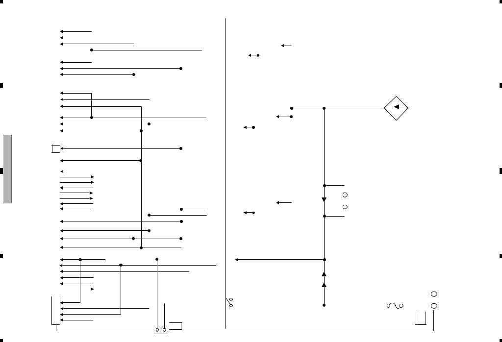
28
1
LX5080D-PDP 3 2
4
F |
|
E |
|
D |
|
C |
|
B |
|
|
|
|
|
|
|
|
|
|
|
|
|
|
|
|
|
|
|
|
|
|
|
|
|
|
|
|
|
|
|
|
|
|
|
|
|
|
|
|
|
|
|
|
|
|
|
|
|
|
|
|
|
|
|
|
|
|
|
|
P1 |
|
|
|
|
|
|
|
|
|
SECONDARY |
|
|
|
|
|
PRIMARY |
|
|
|
|
|
|
|
|
|
|
|
|
|
|
|
|
|
|
|
|
|
|
||||||||||||||
|
|
|
|
|
|
|
+16.5V |
|
|
|
|
|
|
|
|
|
|
|
|
|
|
|
|
|
Switching |
|
|
|
|
|
|
|
|
|
|
|
|
|
|
|
|
|
|
|
|
|
|
||||||||
|
|
|
|
|
|
|
|
|
|
|
|
|
|
|
|
|
|
|
|
|
|
|
|
|
|
|
|
|
|
|
|
|
|
|
|
|
|
|
|
|
|
|
|
|
|
||||||||||
|
|
|
|
|
|
|
+6.5V |
|
|
|
|
|
|
T701 |
|
|
|
|
|
|
|
|
|
Q701 |
|
|
|
|
|
|
|
|
|
|
|
|
|
|
|
|
|
|
|
|
|
|
|
||||||||
|
|
|
|
|
|
|
VSUS |
|
|
|
|
|
|
|
|
|
|
|
|
|
|
|
|
|
|
|
|
|
|
|
|
|
|
|
|
|
|
|
|
|
|
|
|
|
|
|
|
|
|||||||
|
|
|
|
|
|
|
|
|
|
|
|
|
|
|
|
|
|
|
|
|
|
|
|
|
|
|
|
|
|
|
|
|
|
|
|
|
|
|
|
|
|
|
|
|
|
|
|
|
|
|
|
|
|
|
|
|
|
|
P2 |
|
|
|
|
|
|
|
|
|
|
|
|
|
|
|
|
|
|
|
|
|
|
|
|
|
|
|
|
|
|
|
|
|
|
|
|
|
|
|
|
|
|
|
|
|
|
|
|
|
|
|
|
|
|
|
|
|
|
|
|
|
|
|
|
|
|
|
|
|
|
|
|
|
|
|
|
|
|
|
|
|
|
|
|
|
|
|
|
|
|
|
|
|
|
|
|
|
|
|
|
|
|
|
|
|
|
|
|
|
|
|
|
|
|
|
+16.5V |
|
|
|
|
|
|
|
|
|
|
|
|
|
|
|
|
|
|
Q702 |
|
|
|
|
|
|
|
|
|
|
|
|
|
|
|
|
|
|
|
|
|
|
|
||||||
|
|
|
|
|
|
|
|
|
|
|
|
|
|
|
|
|
|
|
|
|
|
|
|
|
|
|
|
|
|
|
|
|
|
|
|
|
|
|
|
|
|
|
|
|
|
|
|||||||||
|
|
|
|
|
|
|
+6.5V |
|
|
|
|
|
|
|
|
|
|
|
|
|
|
|
|
|
Switching |
|
|
|
|
|
|
|
|
|
|
|
|
|
|
|
|
|
|
|
|
|
|
||||||||
|
|
|
|
|
|
|
|
|
|
|
|
|
|
|
|
|
|
|
|
|
|
|
|
|
|
|
|
|
|
|
|
|
|
|
|
|
|
|
|
|
|
||||||||||||||
|
|
|
|
|
|
|
|
|
|
|
|
|
|
|
|
|
|
|
|
|
|
|
|
|
|
|
|
|
|
|
|
|
|
|
|
|
|
|
|
|
|
|
|
|
|
|
|
|
|
|
|||||
|
|
|
|
|
|
|
|
|
|
|
|
|
|
|
|
|
|
|
|
|
|
|
|
|
|
|
|
|
|
|
|
|
|
|
|
|
|
|
|
|
|
|
|
|
|
|
|
|
|
D101 |
|
|
|
||
|
|
|
|
|
|
|
|
|
|
|
|
|
|
|
|
|
|
|
|
|
|
|
|
|
|
|
|
|
|
|
|
|
|
|
|
|
|
|
|
|
|
|
|
|
|
|
|
|
|
|
|
|
|||
|
|
|
|
|
|
|
|
|
|
|
|
|
|
|
|
|
|
|
|
|
|
|
|
|
|
|
|
|
|
|
|
|
|
|
|
|
|
|
|
|
|
|
|
|
|
|
|
|
|
|
|
|
|||
|
|
|
P7 |
|
|
|
|
|
|
|
|
|
|
|
|
|
|
|
|
|
|
|
|
|
|
|
|
|
|
|
|
|
|
|
|
|
|
|
|
|
|
|
|
|
|
|
|
|
|
|
|
||||
|
|
|
|
|
|
|
|
|
|
|
|
|
|
|
|
|
|
|
|
|
|
|
|
|
|
|
|
|
|
|
|
+390V |
|
PFC Q101 |
|
|
|
|
|
|
|
|
|
||||||||||||
|
|
|
|
|
|
|
|
|
|
|
|
|
|
|
|
|
|
|
|
|
|
|
|
|
|
|
|
|
|
|
|
|
|
|
|
|
|
|
|
|
|
|
|
|
|
|
|
||||||||
|
|
|
|
|
|
|
+12V |
|
|
|
|
|
|
|
|
|
|
|
|
|
|
|
|
|
|
|
|
|
|
|
|
|
|
|
|
|
Q102 |
|
|
|
|
|
|
|
|
|
|
|
|
|
|||||
|
|
|
|
|
|
|
|
|
|
|
|
|
|
|
|
|
|
|
|
|
|
|
|
|
|
|
|
|
|
|
|
|
|
|
|
|
|
|
|
|
|||||||||||||||
|
|
|
|
|
|
|
+5.1V |
|
|
|
|
|
|
|
|
|
|
|
|
|
|
|
|
|
|
|
|
|
|
|
|
|
|
|
|
|
Q103 |
|
|
|
|
|
|
|
|
|
|
|
|
|
|||||
|
|
|
|
|
|
|
|
|
|
|
|
|
|
|
|
|
|
|
|
|
|
|
|
|
|
|
Switching |
|
|
|
|
|
|
|
|
|
|
|
|
|
|
|
|
|
|
|
|
|
|
||||||
|
|
|
|
|
|
|
|
|
|
|
|
|
|
|
|
|
|
|
|
|
|
|
|
|
|
|
|
|
|
|
|
|
|
|
|
|
|
|
|
|
|
|
|
|
|
|
|
|
|||||||
|
|
|
P6 |
|
|
|
+60V |
|
|
|
|
|
|
|
|
|
|
|
|
|
|
|
|
|
|
|
|
|
|
|
|
|
|
|
|
|
|
|
|
|
|
|
|||||||||||||
|
|
|
|
|
|
|
|
|
|
|
|
|
|
T901 |
|
|
|
|
|
|
|
Q901 |
|
|
|
|
|
|
|
|
|
|
|
|
|
|
|
|
|
|
|
|
|
|
|
|
|
||||||||
|
|
|
|
|
|
|
|
|
|
|
|
|
|
|
|
|
|
|
|
|
|
|
|
|
|
|
|
|
|
|
|
|
|
|
|
|
|
|
|
|
|
|
|
|
|||||||||||
|
|
|
|
|
|
|
+12V |
|
|
|
|
|
|
|
|
|
|
|
|
|
|
|
|
|
|
|
|
|
|
|
|
|
|
|
|
|
|
|
|
|
|
|
|
|
|
|
|
|
|||||||
|
|
|
|
|
|
|
|
|
|
|
|
|
|
|
|
|
|
|
|
|
|
|
|
|
|
|
|
|
|
|
|
|
|
|
|
|
|
|
|
|
|
|
|
|
|
|
|
|
|
|
|||||
|
|
|
|
|
|
|
+5.1V |
|
|
|
|
|
|
|
|
|
|
|
|
|
|
|
|
|
|
|
|
|
|
|
|
|
|
|
|
|
|
|
|
|
|
|
|
|
|
|
|
|
|
|
|
||||
|
|
|
|
|
|
|
|
|
|
|
|
|
|
|
|
|
|
|
|
|
|
|
|
|
|
|
|
|
|
|
|
|
|
|
|
|
|
|
|
|
|
|
|
|
|
|
|
|
|
|
|
||||
|
|
|
|
|
|
|
|
|
|
|
|
|
|
|
|
|
|
|
|
|
|
|
|
|
|
|
|
Q902 |
|
|
|
|
|
|
|
|
|
|
|
|
|
|
|
|
|
|
|
|
|
|
|
|
|
||
|
|
|
|
|
|
|
|
|
|
|
|
|
|
|
|
|
|
|
|
|
|
|
|
|
|
|
|
|
|
|
|
|
|
|
|
|
|
|
|
|
|
|
|
|
|
|
|
|
|
|
|
|
|||
|
|
|
P5 |
|
|
|
+16.5V |
|
|
|
|
|
|
|
|
|
|
|
|
|
|
|
Switching |
|
|
|
|
|
|
|
|
|
|
|
|
|
|
|
|
|
|
|
|
|
|
||||||||||
|
|
|
|
|
|
|
|
|
|
|
|
|
|
|
|
|
|
|
|
|
|
|
|
|
|
|
|
|
|
|
|
|
|
|
|
|
|
|
|
|
|
||||||||||||||
|
|
|
|
|
|
|
|
|
|
|
|
|
|
|
|
|
|
|
|
|
|
|
|
|
|
|
|
|
|
|
|
|
|
|
|
|
|
|
|
|
|
|
|||||||||||||
|
|
|
|
|
|
|
|
|
|
|
|
|
|
|
|
|
|
|
|
|
|
|
|
|
|
|
|
|
|
|
|
|
|
|
|
|
|
|
|
|
|
|
|
|
|
|
|
|
|
|
|||||
|
|
|
|
|
|
|
|
|
|
|
|
|
|
|
|
|
|
|
|
|
|
|
|
|
|
|
|
|
|
|
|
|
|
|
|
|
|
|
|
|
|
|
|
|
|
|
|
|
|
|
|
|
|
|
|
|
|
|
P4 |
|
|
|
+5.1V |
|
|
|
|
|
|
|
|
|
|
|
|
|
|
|
|
|
|
|
|
|
|
|
|
|
|
|
|
|
|
|
|
|
|
|
|
|
|
|
|
|
|
|
|
||||
|
|
|
|
|
|
|
|
|
|
|
|
|
|
|
|
|
|
|
|
|
|
|
|
|
|
|
|
|
|
|
|
|
|
|
|
|
|
|
|
|
|
|
|
|
|
|
|
|
|
|
|||||
|
|
|
|
|
|
|
DRF_SW_B |
|
|
|
|
|
|
|
|
|
|
|
|
|
|
|
|
|
|
|
|
|
|
|
|
|
|
|
|
|
|
|
|
|
|
|
|
|
|
|
|
|
|
|
|
||||
|
|
|
|
|
|
|
|
|
|
|
|
|
|
|
|
|
|
|
|
|
|
|
|
|
|
|
|
|
|
|
|
|
|
|
|
|
|
|
|
|
|
|
|
|
|
|
|
|
|
|
|||||
|
|
|
|
|
|
|
M_SW_DET |
|
|
|
|
|
|
|
|
|
|
|
|
|
|
|
|
|
|
|
|
|
|
|
|
|
|
|
|
|
|
|
|
|
|
|
|
|
|
|
|
|
|
|
|
||||
|
|
|
|
|
|
|
EXT_PD |
|
|
|
|
|
|
|
|
|
|
|
|
|
|
|
|
|
|
|
|
|
|
|
|
|
|
|
|
|
|
|
|
|
|
|
|
|
|
|
|
|
|
|
|
||||
|
|
|
|
|
|
|
VSUS_ADJ |
|
|
|
|
|
|
|
|
|
|
|
|
|
|
|
|
|
|
|
|
|
|
|
|
|
|
|
|
|
|
|
|
|
|
|
|
|
|
|
|
|
|
|
|
||||
|
|
|
|
|
|
|
PS_PD |
|
|
|
|
|
|
|
|
|
|
|
|
|
|
|
|
|
|
|
|
|
|
|
|
|
|
|
|
|
|
|
|
|
|
|
|
|
|
|
|
|
|
|
|
||||
|
|
|
|
|
|
|
|
|
|
|
|
|
|
|
|
|
|
|
|
|
|
|
|
|
|
|
|
|
|
|
|
|
|
|
|
P11 |
|
|
|
|
|
|
|
|
|
|
|
|
|
||||||
|
|
|
|
|
|
|
RELAY |
|
|
|
|
|
|
|
|
|
|
|
|
|
|
|
Switching |
|
|
D109 |
|
|
|
|
|
|
|
|
|
|
|
|
|
|
|
|
|
||||||||||||
|
|
|
|
|
|
|
DRF_B |
|
|
|
|
|
+35V |
|
|
|
|
|
|
|
|
|
|
|
|
|
|
|
|
|
|
|
|
|
|
|
|
|
|
|
|
|
|
|
|||||||||||
|
|
|
|
|
|
|
|
|
|
|
|
|
T501 |
|
|
|
|
|
|
|
Q501 |
|
|
|
|
|
|
|
|
|
|
|
|
|
|
|
|
|
|
|
|
|
|
|
|
|
|||||||||
|
|
|
|
|
|
|
AC_DET |
|
|
|
|
|
|
|
|
|
|
|
|
|
|
|
|
|
|
|
|
|
|
|
|
|
|
|
|
|
|
|
|
|
|
|
|
|
|
||||||||||
|
|
|
|
|
|
|
PD_TRIG_B |
|
|
|
|
|
+16.5V |
|
|
|
|
|
|
|
|
|
|
|
|
|
|
|
|
|
|
|
|
|
|
|
|
|
|
|
|
|
|
|
|
|
|
|
|
|
|||||
|
|
|
P8 |
|
+16.5V |
|
|
|
|
|
+12V |
|
|
|
|
|
|
|
|
|
|
|
|
|
|
|
|
|
|
|
|
|
|
|
|
|
|
|
|
|
|
|
|
|
|
|
|
|
|
||||||
|
|
|
|
|
+12V |
|
|
|
|
|
|
|
|
|
|
|
|
|
|
|
|
Q502 |
|
|
|
|
|
|
|
|
|
|
|
|
|
|
|
|
|
|
|
|
|
|
|
|
|
||||||||
|
|
|
|
|
|
|
|
|
|
|
|
|
|
|
|
|
|
|
|
|
|
|
|
|
|
|
|
|
|
|
|
|
|
|
|
|
|
|
|
|
|
|
|
|
|
||||||||||
|
|
|
|
|
|
|
|
|
|
|
|
|
|
|
|
|
|
|
|
Switching |
|
|
|
|
|
|
|
|
|
|
|
|
|
|
|
|
|
|
|
|
|
|
|||||||||||||
|
|
|
|
|
+6.5V |
|
|
|
|
|
|
|
|
|
|
|
|
|
|
|
|
|
|
|
|
|
|
|
|
|
|
|
|
|
|
|
|
|
|
|
|
|
|
|
|
|
|
|
|
||||||
|
|
|
|
|
|
T401 |
|
|
|
|
|
|
|
|
|
|
|
|
|
|
|
|
|
|
|
|
|
|
|
|
|
|
|
|
|
|
|
|
|
|
|
|
|
|
|
|
|
||||||||
|
|
|
|
|
|
|
|
|
|
|
|
|
|
|
|
|
|
|
|
|
|
|
|
|
|
|
|
|
|
|
|
|
|
|
|
|
|
|
|
|
|
|
|
|
|
|
|
|
|
|
|
|
|
||
|
|
|
|
|
+5.1V |
|
T402 |
|
|
|
|
|
|
|
|
|
|
|
|
|
|
|
|
|
|
|
|
|
|
|
|
|
|
|
|
|
|
|
|
|
|
|
|
|
|
|
|
|
|||||||
|
|
|
|
|
|
|
|
|
|
|
|
|
|
|
|
|
|
|
|
|
|
|
|
|
|
|
|
|
|
|
|
|
|
|
|
|
|
|
|
|
|
|
|
|
|
|
|
|
|
|
|
|
|
||
|
|
|
P9 |
|
STB5.1V |
|
|
|
|
|
|
|
|
|
|
|
|
|
|
|
|
|
|
|
|
|
|
|
|
|
|
|
|
|
|
|
|
|
|
|
|
|
|
|
|
|
|
|
|
|
|
|
|
||
|
|
|
|
|
STB3.3V |
IC202 |
|
|
|
|
|
|
|
|
|
|
|
T101 |
|
|
|
|
|
|
|
|
|
|
|
|
|
|
|
|
|
|
|
|
|
|
|
|
|
|
|
|
|
|
|
|
|
|
|
||
|
|
|
|
|
|
|
|
|
|
|
|
|
|
|
|
|
|
|
|
|
|
|
|
|
|
|
|
|
|
|
|
|
|
|
|
|
|
|
|
|
|
|
|
|
|
|
|
|
|
|
|||||
|
|
|
|
|
|
Q203 |
|
|
|
|
|
|
|
|
|
|
|
|
|
|
|
|
|
|
|
|
|
|
|
|
|
|
|
|
|
|
|
|
|
|
|
|
|
|
|
|
|
|
|
|
|
||||
|
|
|
|
|
+35V |
|
|
|
|
|
|
|
|
|
|
|
|
|
|
|
|
|
|
IC101 |
|
|
|
|
|
|
|
|
|
|
|
|
|
|
|
|
|
|
|
|
|
|
|
|
|||||||
|
|
|
|
|
|
|
|
|
|
|
|
|
|
|
|
|
|
|
|
|
|
|
|
Switching |
|
|
|
D106 |
|
|
|
|
|
|
|
|
|
|
|
|
|||||||||||||||
|
|
|
|
|
|
|
M_SW_DET |
|
|
|
|
|
|
|
|
|
|
|
|
|
|
|
|
|
|
|
|
|
|
|
|
|
|
|
|
|
|
|
|
||||||||||||||||
|
|
|
|
|
|
|
|
|
|
|
|
|
|
|
|
|
|
|
|
|
|
|
|
|
|
|
|
|
|
|
|
|
|
|
|
|
|
|
|
|
|
|
|
|
|
|
|
|
|
|
|||||
|
|
|
|
|
|
|
AC_DET |
|
|
|
|
|
|
|
|
|
|
|
|
|
|
|
|
|
|
|
|
|
|
|
|
|
D108 |
|
|
|
|
|
|
|
|
|
|
|
|
||||||||||
|
|
|
|
|
|
|
|
|
|
|
|
|
|
|
|
|
|
|
|
|
|
|
|
|
|
|
|
|
|
|
|
|
|
|
|
|
|
|
|
|
|
|
|||||||||||||
|
|
|
|
|
|
|
US_SW |
|
|
|
|
|
|
|
|
|
|
|
|
|
|
|
|
|
|
|
|
|
|
|
|
|
|
|
|
|
|
|
|
|
|
|
|
|
|
NEUTRAL |
|
|
|
||||||
|
|
|
|
|
|
|
|
|
|
|
|
|
|
|
|
|
|
|
|
|
|
|
|
|
|
|
|
|
|
|
|
|
|
|
|
|
|
|
|
|
|
|
|
|
|||||||||||
|
|
|
|
|
|
|
|
|
|
|
|
|
|
|
|
|
|
|
|
|
|
|
|
|
|
|
|
|
|
|
|
|
|
|
|
|
|
|
|
|
|
|
|
|
|
|
|
|
|
|
|
|
|
|
|
|
|
|
P12 |
|
STB5.1V |
|
|
|
|
|
|
|
|
|
|
|
|
|
|
|
|
|
|
|
|
|
|
|
|
|
|
|
|
|
|
|
|
|
|
|
|
|
|
LIVE |
|
|
|
||||||||
|
|
|
|
|
|
|
|
|
|
|
|
|
|
|
|
|
|
|
|
|
|
|
|
|
|
|
|
|
|
|
|
|
|
|
|
|
|
|
|
|
|
|
|
|
|
||||||||||
|
|
|
|
|
|
|
|
|
|
|
|
|
|
|
|
|
|
|
|
|
|
|
|
|
|
|
|
|
|
|
|
|
|
|
|
|
|
|
|
|
|
|
|
|
|
||||||||||
|
|
|
|
|
+12V |
|
|
+B for Relay Drive |
|
|
|
|
|
|
|
|
|
|
|
|
|
|
|
|
|
|
|
|
|
|
|
|
|
|
|
|
|
|
|
|
|
||||||||||||||
|
|
|
|
|
|
|
|
|
|
|
|
|
|
|
|
|
|
|
|
|
|
|
|
|
|
|
|
|
|
|
|
|
|
|
|
|
|
|
|
|
|
|
|||||||||||||
|
|
|
|
|
STB3.3V |
|
|
|
|
|
|
|
|
|
|
|
|
|
|
|
|
|
|
|
|
|
|
|
|
|
|
|
|
|
|
|
|
|
|
|
|
|
|
||||||||||||
|
|
|
|
|
|
|
|
|
|
|
|
|
|
|
|
|
|
|
|
|
|
|
|
|
|
|
|
|
|
|
|
|
|
|
|
|
|
|
|
||||||||||||||||
|
|
|
|
|
|
|
|
|
|
|
|
|
|
RY102 |
|
|
|
|
|
|
|
|
|
|
|
F101 |
|
|
|
||||||||||||||||||||||||||
|
|
|
|
|
|
|
|
|
|
|
|
|
|
|
|
|
|
|
|
|
|
|
|
|
|
|
|
|
|
|
|
|
|
|
|||||||||||||||||||||
|
|
|
|
|
|
|
AC_DET |
|
|
|
|
|
|
|
|
|
|
|
|
|
|
|
|
|
|
|
|
|
|
|
|
|
|
|
|
|
|
|
|
|
|
|
|
|
|
|
P3 |
|
|
|
|||||
|
|
|
|
|
|
|
|
|
|
|
|
|
|
|
|
|
|
|
|
|
|
|
|
|
|
|
|
|
|
|
|
|
|
|
|
|
|
|
|
|
|
|
|
|
|
|
|
|
|
|
|||||

 P10
P10
|
A |
UNIT SUPPLY POWER |
SUPPLY POWER 5.4 |
|
UNIT |
1
2
3
4

|
5 |
|
6 |
|
7 |
|
8 |
|
4.6 50F X DRIVE ASSY
A
50F X DRIVE ASSY |
|
|
|
|
|
|
|
|
|||
+60V +12V +5.1V |
+60V |
+8V |
+3.3V |
+60V |
+8V +3.3V |
|
VSUS |
|
|||
|
|
|
|
|
|
|
|
|
|
|
B |
X 7 |
|
X 4 |
|
|
X 3 |
|
|
|
SUS |
|
|
|
|
|
|
|
|
|
|
|
|
BLOCK |
|
+12V |
REGULATOR |
|
+8V |
|
|
+16.5 |
VSUS |
|
|
||
+5.1V |
REGULATOR |
|
+3.3V |
|
|
|
|
|
|
||
|
|
|
|
|
|
+5V |
|
XPRST |
|
|
|
VSUS |
+16.5V +6.5V |
|
|
|
|
|
|
VSUS |
|
||
|
|
|
|
|
|
|
|
|
|||
|
|
|
REGULATOR |
|
|
|
|
|
|
||
|
|
|
X 2 |
+16.5V |
|
|
|
SUS |
PSUS |
||
|
|
|
|
|
|
|
|||||
|
|
|
|
|
|
|
|
BLOCK |
C |
||
+5V |
|
|
|
|
|
|
|
|
|
||
|
|
|
|
|
|
|
|
|
|
|
|
|
Drive Signal |
SUS |
|
Gate Signal |
|
+16.5 |
|
||||
X 1 |
|
|
|
|
PreDrive |
|
|
|
|
|
|
|
|
|
|
|
+16.5V |
|
|
|
|
||
|
|
|
|
|
PU |
|
|
SOFT-D |
|
||
|
|
|
|
|
|
|
|
|
|
||
|
Drive Signal |
RESONANCE |
PSUS |
|
|
|
|||||
LOGIC |
|
|
|
|
|
|
|
||||
BLOCK |
|
|
|
BLOCK |
|
+16.5 |
|
|
|
||
|
Drive Signal |
|
|
|
OFFSET |
|
D |
||||
|
|
|
|
|
|
|
|
|
|
||
|
|
|
|
|
|
|
|
BLOCK |
VSUS |
PSUS |
|
|
|
|
|
|
VPOFS |
|
|
|
|||
|
|
|
|
|
|
|
|
|
|
||
|
VPOFS |
VPU |
|
|
|
VXKOFS1 |
|
|
|
||
|
|
|
|
|
|
|
|
|
SUS |
|
|
|
|
|
|
|
OFFSET |
|
VXKOFS2 |
|
BLOCK |
|
|
|
|
15V |
|
|
|
|
|
||||
|
|
|
Reg. |
|
|
|
|
|
|||
+16.5V |
DC/DC |
|
|
|
|
|
|
|
|
||
|
|
CONV. |
|
|
|
|
|
|
VSUS |
|
|
X 6 |
|
X 5 |
|
|
|
|
|
|
|
|
|
|
|
|
|
|
|
|
|
|
|
SUS |
E |
|
|
|
|
|
|
|
|
|
|
BLOCK |
|
+60V +8V |
+3.3V |
+60V +8V |
+3.3V |
|
|
|
|
|
|
||
|
|
|
|
|
|
|
|
|
|
|
F |
|
|
|
|
|
|
|
|
PDP-LX5080D |
|
29 |
|
|
|
|
|
|
|
|
|
|
|
||
5 |
|
|
|
|
|
6 |
|
|
|
7 |
8 |
|
1 |
|
2 |
|
3 |
|
4 |
|
4.7 50F Y DRIVE, 50F SCAN A, B, C and D ASSYS
A
50F SCAN B ASSY (HIGH-SIDE_LOW)
|
50F SCAN A ASSY |
||||
|
(HIGH-SIDE_HIGH) |
||||
|
VH |
IC5V |
Scan Signal |
|
|
|
|
|
|
|
|
|
Scan IC |
PSUS |
|
|
|
|
IC2804 |
|
|
||
|
|
|
|
||
|
VH |
IC5V |
|
|
|
|
Scan IC |
|
|
|
|
|
IC2803 |
|
|
|
|
B |
VH |
IC5V |
|
|
|
|
|
|
|
|
|
|
Scan IC |
|
|
|
|
|
IC2802 |
|
|
|
|
|
VH |
IC5V |
|
|
|
|
Scan IC |
|
|
|
|
|
IC2801 |
|
|
|
|
|
|
|
SA1 |
|
|
|
VH |
IC5V |
SB2 |
|
|
|
Scan IC |
|
|
|
|
|
IC2904 |
|
|
|
|
|
VH |
IC5V |
|
|
|
|
Scan IC |
|
|
|
|
|
IC2903 |
|
|
|
|
|
VH |
IC5V |
|
|
|
C |
Scan IC |
|
|
|
|
IC2902 |
|
|
|
||
|
VH |
IC5V |
|
|
Scan Signal |
|
|
|
|
|
|
|
Scan IC |
|
|
VH |
|
|
IC2901 |
|
|
IC5V |
|
|
|
|
|
SB1 |
|
|
VH |
IC5V |
Scan Signal |
SC1 |
Scan Signal |
|
|
|
|||
|
Scan IC |
PSUS |
|
VH |
|
|
IC3004 |
|
IC5V |
||
|
VH |
IC5V |
|
|
|
|
Scan IC |
|
|
|
|
|
IC3003 |
|
|
|
|
|
VH |
IC5V |
|
|
|
|
Scan IC |
|
|
|
|
|
IC3002 |
|
|
|
|
D |
VH |
IC5V |
|
|
|
|
|
|
|
|
|
|
Scan IC |
|
|
|
|
|
IC3001 |
|
|
|
|
|
|
|
SC2 |
|
|
|
VH |
IC5V |
SD1 |
|
|
|
|
|
|
|
|
|
Scan IC |
|
|
|
|
|
IC3104 |
|
|
|
|
|
VH |
IC5V |
|
|
|
|
Scan IC |
|
|
|
|
|
IC3103 |
|
|
|
|
|
VH |
IC5V |
|
|
|
|
Scan IC |
|
|
|
|
|
IC3102 |
|
|
|
|
|
VH |
IC5V |
|
|
|
E |
Scan IC |
|
|
|
|
IC3101 |
|
|
|
||
50F SCAN D ASSY (LOW-SIDE_LOW)
50F SCAN C ASSY (LOW-SIDE_HIGH)
50F Y DRIVE ASSY
|
|
|
|
|
|
|
|
|
|
|
|
Y 6 |
|
+16.5V |
|
VSUS |
|
|
|
|
|
+8V |
|
||
|
|
|
|
|
|
|
|
+3.3V |
VADR |
|||
|
|
|
|
|
|
|
|
|
|
|||
|
RST-D |
|
SUS |
|
|
|
|
|
|
|
Y 7 |
|
|
|
|
|
|
|
|
|
|
|
|||
|
BLOCK |
|
BLOCK |
|
VC_S |
|
|
+8V |
|
|||
|
|
|
|
|
|
|
|
+3.3V |
VADR |
|||
|
|
|
|
|
|
+16.5V |
VKNOFS4 |
|
||||
|
VC_P VYPRST |
|
|
|
|
|
|
|
||||
|
|
|
|
|
|
|
|
|
|
|
||
|
|
|
|
|
|
KNOFS4 |
|
|
+3.3V +8V VADR |
|||
|
|
|
|
|
|
|
|
|
|
|
||
|
PRST |
|
|
|
SOFT-G |
|
|
REG |
|
|||
|
BLOCK |
|
|
|
BLOCK |
|
|
+5.1V |
REG |
|||
|
|
|
|
|
|
|
|
|
|
|||
|
VC_U |
+16.5V |
|
|
|
VSNOFS |
|
|
Y 5 |
|
12V |
|
|
|
|
|
|
|
|
|
|||||
|
|
|
|
|
|
+16.5V |
VKNOFS2 |
|
|
|
|
|
PSUS |
RESONANCE |
|
|
|
|
|
VC_S |
|
+5V |
|
|
|
BLOCK |
|
MSK-S |
|
SNOFS |
|
|
|
|
||||
|
|
|
|
|
|
|
|
|||||
|
|
|
|
|
|
|
+16.5V |
VSUS |
||||
|
|
|
|
|
|
KNOFS2 |
|
|
||||
|
|
|
|
|
|
Drive Signal |
REG |
|
|
|||
|
VC_S |
VC_S |
|
|
|
BLOCK |
+6.5V |
|
|
|||
|
|
|
|
|
|
|
|
|||||
Y 2 |
|
|
|
|
|
|
|
|
|
|
|
|
|
|
|
|
Gate Signal |
|
|
|
|
|
|
|
|
VH |
|
|
SUSOUT |
|
|
|
|
|
|
|
Y 4 |
|
IC5V |
|
|
|
|
|
|
|
|
|
|
||
|
|
|
VSUS |
|
|
|
|
|
|
|
||
|
H-MSK |
L-MSK |
|
+16.5V |
|
+5V |
|
|
|
|||
|
|
|
|
|
|
|
|
|
||||
|
|
SUS |
|
SUS |
Drive Signal |
|
|
|
|
|||
|
|
|
|
|
|
|
|
|
||||
VH |
|
|
|
BLOCK |
PreDrive |
|
|
|
|
|
|
|
IC5V |
|
|
|
|
|
|
|
|
|
|
|
|
Y 3 |
|
|
|
|
|
|
Drive Signal |
LOGIC |
|
|
|
|
|
|
|
|
|
|
|
|
|
|
|
||
|
|
|
|
|
|
|
|
BLOCK |
|
|
|
|
|
|
|
|
|
|
VYPRST |
|
|
|
|
||
|
VC_U |
+16.5V |
|
VSUS |
|
|
|
|
|
|
||
|
|
|
VSNOFS |
VKNOFS1 |
|
|
|
|
||||
|
|
|
|
|
|
|
|
|
|
|||
PSUS |
|
|
|
SUS |
|
|
|
VH |
|
|
Y 1 |
|
RESONANCE |
|
|
MAIN |
|
|
|
|
|||||
|
VSUS |
|
|
|
|
|
||||||
|
|
BLOCK |
|
|
|
|
|
|||||
|
BLOCK |
|
DC/DC |
|
|
|
|
|
||||
|
|
|
|
|
|
|
|
|
||||
|
|
|
|
|
|
CONV. |
|
|
|
|
|
|
|
VKNOFS1 |
|
|
|
|
|
|
|
|
|
|
|
|
+16.5V |
VKNOFS3 |
|
|
VKNOFS2 |
VKNOFS4 |
|
|
|
|
||
|
|
|
|
|
|
VKNOFS3 |
|
|
|
|
|
|
|
|
|
|
|
+16.5V VC_S VC_U +16.5V IC5V VC_P |
|
|
|
||||
|
KNOFS1 |
|
VSUS |
|
|
|
|
|
+3.3V |
VADR |
||
|
KNOFS3 |
|
|
|
|
|
|
|
||||
|
|
|
|
|
|
|
|
|
+8V |
|
||
|
BLOCK |
|
SUS |
|
15V |
|
IC5V/VF |
|
Y 8 |
|
|
|
|
|
|
|
DC/DC |
|
DC/DC |
|
|
|
|
||
|
|
|
|
BLOCK |
|
|
|
|
|
|||
|
|
IC5V |
|
CONV. |
|
CONV. |
|
+3.3V |
VADR |
|||
|
|
|
|
|
|
|
|
|
|
|||
|
Photo Coupler |
|
|
Scan Signal |
|
|
|
Y 9 |
+8V |
|||
|
|
|
|
|
|
|
|
|||||
|
|
BLOCK |
|
|
|
|
|
|
|
|
|
|
F
30 |
|
|
PDP-LX5080D |
|
|
|
|
|||
|
1 |
|
2 |
|
|
|
3 |
|
4 |
|
|
|
|
|
|
|
|
||||
Loading...