


ORDER NO.
ARP3174
PDP-434PU
PLASMA DISPLAY
PDP-434PU
PDP-434PE
PRO-434PU
THIS MANUAL IS APPLICABLE TO THE FOLLOWING MODEL(S) AND TYPE(S).
Model |
Type |
Power Requirement |
Remarks |
|
|
|
|
PDP-434PU |
TUCK |
AC110 - 240V |
|
|
|
|
|
PDP-434PE |
WYVI6 |
AC220 - 240V |
|
|
|
|
|
PDP-434PE |
WYVI6XK |
AC220 - 240V |
|
|
|
|
|
PRO-434PU |
KUC |
AC120V |
|
|
|
|
|
This service manual should be used together with the following manual(s).
Model No. |
Order No. |
Remarks |
|
|
|
PDP-434PU/ TUCK |
ARP3175 |
SCHEMATIC DIAGRAM and PCB CONNECTION DIAGRAM |
PDP-434PE/ WYVI6 |
|
|
PDP-434PE/ WYVI6XK |
|
|
PRO-434PU/ KUC |
|
|
|
|
|
Confirm it
Serial No.
 WYVI6
WYVI6 
 SS
SS


For details, refer to "Important symbols for good services". |
WYVI6XK |
UK |
PIONEER CORPORATION 4-1, Meguro 1-chome, Meguro-ku, Tokyo 153-8654, Japan
PIONEER ELECTRONICS (USA) INC. P.O. Box 1760, Long Beach, CA 90801-1760, U.S.A.
PIONEER EUROPE NV Haven 1087, Keetberglaan 1, 9120 Melsele, Belgium
PIONEER ELECTRONICS ASIACENTRE PTE. LTD. 253 Alexandra Road, #04-01, Singapore 159936
 PIONEER CORPORATION 2003
T-ZZY SEPT. 2003 printed in Japan
1 |
2 |
3 |
4 |
SAFETY INFORMATION
A |
|
|
|
|
|
|
|
|
|
|
This service manual is intended for qualified service technicians ; it is not meant for the casual |
||||||||||
do-it-yourselfer. Qualified technicians have the necessary test equipment and tools, and have been |
||||||||||
trained to properly and safely repair complex products such as those covered by this manual. |
||||||||||
Improperly performed repairs can adversely affect the safety and reliability of the product and may |
||||||||||
void the warranty. If you are not qualified to perform the repair of this product properly and safely, |
||||||||||
you should not risk trying to do so and refer the repair to a qualified service technician. |
||||||||||
WARNING |
|
|
|
|
|
|
|
|
|
|
This product contains lead in solder and certain electrical parts contain chemicals which are known to the state of California to |
||||||||||
cause cancer, birth defects or other reproductive harm. |
|
|
|
|
||||||
B |
|
|
|
|
|
|
|
|
|
Health & Safety Code Section 25249.6 - Proposition 65 |
NOTICE |
|
|
|
|
|
|
|
|
|
|
(FOR CANADIAN MODEL ONLY) |
|
|
|
|
||||||
Fuse symbols |
|
(fast operating fuse) and/or |
|
(slow operating fuse) on PCB indicate that replacement parts |
||||||
|
|
|||||||||
must be of identical designation. |
|
|
|
|
|
|
||||
REMARQUE |
|
|
|
|
|
|
|
|
|
|
(POUR MODÈLE CANADIEN SEULEMENT) |
|
|
|
|
||||||
Les symboles de fusible |
|
|
(fusible de type rapide) et/ou |
|
|
(fusible de type lent) sur CCI indiquent que les pièces |
||||
|
|
|
||||||||
de remplacement doivent avoir la même désignation. |
|
|
|
|
||||||
C |
|
|
|
|
|
|
|
|
|
|
|
SAFETY PRECAUTIONS |
|
|
|
NOTICE : Comply with all cautions and safety related notes |
6. |
Perform the following precautions against unwanted radiation |
|
located on or inside the cabinet and on the chassis. |
|
and rise in internal temperature. |
|
The following precautions should be observed : |
• Always return the internal wiring to the original styling. |
|
|
1. When service is required, even though the PDP UNIT an |
• Attach parts (Gascket, Ferrite Core, Ground, Rear Cover, |
|
|
isolation transformer should be inserted between the power line |
|
Shield Case etc.) surely after disassembly. |
D |
and the set in safety before any service is performed. |
7. |
Perform the following precautions for the PDP panel. |
2. When replacing a chassis in the set, all the protective devices |
• When the front case is removed, make sure nothing hits the |
||
|
must be put back in place, such as barriers, nonmetallic knobs, |
|
panel face, panel corner, and panel edge (so that the glass does |
|
adjustment and compartment covershields, isolation resistor- |
|
not break). |
|
capacitor, etc. |
• Make sure that the panel vent does not break. (Check that the |
|
|
3. When service is required, observe the original lead dress. Extra |
|
cover is attached.) |
|
precaution should be taken to assure correct lead dress in the |
• Handle the FPC connected to the panel carefully. |
|
|
high voltage circuitry area. |
|
Twisting or pulling the FPC when connecting it to the |
|
4. Always use the manufacture's replacement components. |
|
connector will cause it to peel off from the panel. |
|
Especially critical components as indicated on the circuit |
8. |
Pay attention to the following. |
|
diagram should not be replaced by other manufacture's. |
• When the front case is removed, infrared ray is radiated and |
|
|
Furthermore where a short circuit has occurred, replace those |
|
may disturb reception of the remote control unit. |
E |
components that indicate evidence of overheating. |
• Pay extreme caution when the front case and rear panel are |
|
5. Before returning a serviced set to the customer, the service |
|
removed because this may cause a high risk of disturbance to |
|
|
|
||
|
technician must thoroughly test the unit to be certain that it is |
|
TVs and radios in the surrounding. |
|
completely safe to operate without danger of electrical shock, |
|
|
|
and be sure that no protective device built into the set by the |
|
|
|
manufacture has become defective, or inadvertently defeated |
|
|
|
during servicing. Therefore, the following checks should be |
|
|
|
performed for the continued protection of the customer and |
|
|
|
servicetechnician. |
|
|
F
|
|
|
|
|
|
|
2 |
|
PDP-434PU |
|
|
||
1 |
2 |
|
|
|
3 |
4 |
5 |
6 |
7 |
8 |
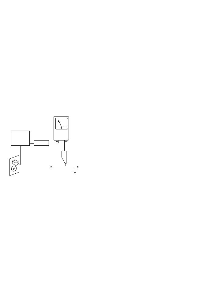
Leakage Current Cold Check
With the AC plug removed from an AC power source, place a jumper across the two plug prongs. Turn the AC power switch on. Using an insulation tester (DC 500V), connect one lead to the jumpered AC plug and touch the other lead to each exposed metal part (input/output terminals, screwheads, metal overlays, control shafts, etc.), particularly any exposed metal part having a return path to the chassis. Exposed metal parts having a return path to the chassis should have a minimum resistor reading of 0.3MΩ and a maximum resistor reading of 5MΩ . Any resistor value below or above this range indicates an abnormality which requires corrective action. Exposed metal parts not having a return path to the chassis will indicate an open circuit.
Leakage Current Hot Check
Plug the AC line cord directly into an AC power source (do not use an isolation transformer for this check).
Turn the AC power switch on.
U s i n g a " L e a k a g e C u r r e n t Te s t e r ( S i m p s o n M o d e l 2 2 9 equivalent)", measure for current from all exposed metal parts of the cabinet (input/output terminals, screwheads, metal overlays, control shaft, etc.), particularly any exposed metal part having a return path to the chassis, to a known earth ground (water pipe, conduit, etc.). Any current measured must not exceed 0.5mA.
|
|
Reading should |
|
Leakage |
not be above |
Device |
current |
0.5mA |
under |
tester |
|
test |
|
|
Test all |
|
|
exposed metal |
|
|
surfaces |
|
|
Also test with |
|
|
plug reversed |
|
Earth |
(Using AC adapter |
|
ground |
plug as required) |
|
|
PRODUCT SAFETY NOTICE
Many electrical and mechanical parts in PIONEER set have special safety related characteristics. These are often not evident from visual inspection nor the protection afforded by them necessarily can be obtained by using replacement components rated for higher voltage, wattage, etc. Replacement parts which have these special safety characteristics are identified in this Service Manual.
Electrical components having such features are identified by marking with a on the schematics and on the parts list in this Service Manual.
The use of a substitute replacement component which dose not h a v e t h e s a m e s a f e t y c h a r a c t e r i s t i c s a s t h e P I O N E E R recommended replacement one, shown in the parts list in this Service Manual, may create shock, fire or other hazards.
Product Safety is continuously under review and new instructions are issued from time to time. For the latest information, always consult the current PIONEER Service Manual. A subscription to, or additional copies of, PIONEER Service Manual may be obtained at a nominal charge from PIONEER.
AC Leakage Test
A
B
C
D
A N Y M E A S U R E M E N T S N O T W I T H I N T H E L I M I T S
OUTLINED ABOVE ARE INDICATIVE OF A POTENTIAL
SHOCK HAZARD AND MUST BE CORRECTED BEFORE
RETURNING THE SET TO THE CUSTOMER.
E
F
|
|
|
|
|
|
|
|
|
PDP |
-434PU |
7 |
3 |
|
5 |
6 |
|
|
|
8 |
|
1 2 3 4
|
|
Charged Section |
|
|
High Voltage Generating Point |
|
|
|
|
|
|
||
A |
The places where the commercial AC power is used without |
The places where voltage is 100V or more except for the charged |
||||
|
passing through the power supply transformer. |
places described above. If the places are touched, there is a risk of |
||||
|
If the places are touched, there is a risk of electric shock. In |
electric shock. |
|
|||
|
addition, the measuring equipment can be damaged if it is |
|
|
|
|
|
|
connected to the GND of the charged section and the GND of the |
1. |
SW POWER SUPPLY Unit...................................... |
(215V) |
||
|
non-charged section while connecting the set directly to the |
2. |
43 X DRIVE Assy ........................................... |
(–225V to 215V) |
||
|
commercial AC power supply. Therefore, be sure to connect the |
3. |
43 Y DRIVE Assy ........................................................... |
(345V) |
||
|
set via an insulated transformer and supply the current. |
4. |
43 SCAN (A) Assy .......................................................... |
(345V) |
||
|
|
|
5. |
43 SCAN (B) Assy .......................................................... |
(345V) |
|
|
|
|
6. X CONNECTOR AAssy ............................ |
(–225V to 215V) |
||
|
1. AC Power Cord |
7. X CONNECTOR B Assy ............................ |
(–225V to 215V) |
|||
|
2. AC Inlet with Filter |
|
|
|
|
|
B3. Power Switch (S1)
4.Fuse (In the POWER SUPPLY Unit)
5.STB Transformer and Converter Transformer
|
(In the POWER SUPPLY Unit) |
|
: Part is Charged Section. |
|
6. Other primary side of the POWER SUPPLY Unit |
|
: Part is the High Voltage Generating Points |
|
|
|
|
|
|
|
other than the Charged Section. |
|
43 Y DRIVE Assy |
POWER SUPPLY Unit |
43 X DRIVE Assy |
C |
43 SCAN |
|
X CONNECTOR |
B Assy |
|
||
|
|
||
|
|
A Assy |
|
|
|
|
43 SCAN
A Assy
D
|
X CONNECTOR |
|
B Assy |
AC Inlet with Filter |
Power Cord |
Power Switch |
|
E |
(S1) |
|
Fig.1 Charged Section and High Voltage Generating Point (Rear View)
F
|
|
|
|
|
|
|
4 |
|
PDP-434PU |
|
|
||
1 |
2 |
|
|
|
3 |
4 |

5 |
6 |
7 |
8 |
[ Important symbols for good services ]
In this manual, the symbols shown-below indicate that adjustments, settings or cleaning should be made securely. When you find the procedures bearing any of the symbols, be sure to fulfill them:
1. Product safety
You should conform to the regulations governing the product (safety, radio and noise, and other regulations), and should keep the safety during servicing by following the safety instructions described in this manual.
2. Adjustments
To keep the original performances of the product, optimum adjustments or specification confirmation is indispensable.
In accordance with the procedures or instructions described in this manual, adjustments should be performed.
3. Cleaning
For optical pickups, tape-deck heads, lenses and mirrors used in projection monitors, and other parts requiring cleaning, proper cleaning should be performed to restore their performances.
4. Shipping mode and shipping screws
A
B
To protect the product from damages or failures that may be caused during transit, the shipping mode should be set or the shipping screws should be installed before shipping out in accordance with this manual, if necessary.
5. Lubricants, glues, and replacement parts
Appropriately applying grease or glue can maintain the product performances. But improper lubrication or applying
 glue may lead to failures or troubles in the product. By following the instructions in this manual, be sure to apply the
 prescribed grease or glue to proper portions by the appropriate amount.For replacement parts or tools, the prescribed ones should be used.
C
D
E
F
|
|
|
|
|
|
|
|
|
PDP |
-434PU |
7 |
5 |
|
5 |
6 |
|
|
|
8 |
|

1 2 3 4
CONTNTS
|
SAFETY INFORMATION...................................................................................................................................................... |
2 |
|
A |
1. SPECIFICATIONS .............................................................................................................................................................. |
7 |
|
2. EXPLODED VIEWS AND PARTS LIST |
8 |
||
|
|||
|
2.1 PACKING ...................................................................................................................................................................... |
8 |
|
|
2.2 CHASSIS SECTION (1) .......................................................................................................................................... |
10 |
|
|
2.3 CHASSIS SECTION (2) .......................................................................................................................................... |
12 |
|
|
2.4 FLAME SECTION .................................................................................................................................................... |
14 |
|
|
2.5 MULTI BASE SECTION .......................................................................................................................................... |
16 |
|
|
2.6 REAR SECTION....................................................................................................................................................... |
18 |
|
|
2.7 FRONT PANEL SECTION ...................................................................................................................................... |
20 |
|
|
2.9 PANEL CHASSIS (43) Assy (AWU1070) ............................................................................................................. |
21 |
|
|
2.9 PANEL CHASSIS (43) Assy (AWU1070) ............................................................................................................. |
21 |
|
B |
3. BLOCK DIAGRAM AND SCHEMATIC DIAGRAM (For SCHEMATIC DIAGRAM, Refer to ARP3175) .................... |
22 |
|
3.1 BLOCK DIAGRAM |
22 |
||
|
|||
|
3.1.1 OVERALL BLOCK DIAGRAM......................................................................................................................... |
22 |
|
|
3.1.2 43 Y DRIVE ASSY ............................................................................................................................................ |
24 |
|
|
3.1.3 43 X DRIVE ASSY ............................................................................................................................................ |
25 |
|
|
3.1.4 PANEL IF ASSY ................................................................................................................................................ |
26 |
|
|
3.1.5 DIGITAL VIDEO ASSY ..................................................................................................................................... |
31 |
|
|
3.1.6 HD AUDIO AMP ASSY .................................................................................................................................... |
33 |
|
|
3.2 WAVEFORMS ........................................................................................................................................................... |
34 |
|
|
4. PCB CONNECTION DIAGRAM (Refer to ARP3175) |
|
|
|
5. PCB PARTS LIST ............................................................................................................................................................ |
39 |
|
C |
6. ADJUSTMENT ................................................................................................................................................................. |
47 |
|
6.1 ADJUSTMENT REQUIRED WHEN THE SET IS REPAIRED OR REPLACED............................................ |
47 |
||
|
6.2 COMMAND................................................................................................................................................................ |
47 |
|
|
6.2.1 RS232C COMMAND........................................................................................................................................ |
47 |
|
|
7. GENERAL INFORMATION ............................................................................................................................................ |
54 |
|
|
7.1 DIAGNOSIS............................................................................................................................................................... |
54 |
|
|
7.1.1 PCB LOCATION ................................................................................................................................................ |
54 |
|
|
7.1.2 DIAGNOSIS OF SHUTDOWN/POWER-DOWN INDICATED BY LEDS................................................. |
55 |
|
|
7.1.3 DIAGNOSIS WITH THE AID OF FACTORY MODE.................................................................................... |
60 |
|
|
7.1.4 CANCELING DETECTION BY THE TRAP SWITCH ................................................................................. |
63 |
|
|
7.1.5 OPERATION WHEN THE MEDIA RECEIVER IS NOT CONNECTED ................................................... |
64 |
|
|
7.1.6 TEMPERATURE-COMPENSATION FUNCTION OF THE DRIVE-SYSTEM VOLTAGE ...................... |
64 |
|
D |
7.1.7 POWER ON/OFF FUNCTION FOR THE LARGE-SIGNAL SYSTEM..................................................... |
65 |
|
|
7.1.8 BACKING UP THE ADJUSTMENT VALUES FOR THE MAIN UNIT....................................................... |
66 |
|
|
7.1.9 TROUBLESHOOTING ..................................................................................................................................... |
68 |
|
|
7.1.10 DISASSEMBLY ............................................................................................................................................... |
69 |
|
|
7.2 IC INFORMATION.................................................................................................................................................... |
72 |
|
|
8. PANEL FACILITIES AND SPECIFICATIONS ............................................................................................................. |
94 |
E
F
|
|
|
|
|
|
|
6 |
|
PDP-434PU |
|
|
||
1 |
2 |
|
|
|
3 |
4 |
5 |
6 |
7 |
8 |
|
|
1. SPECIFICATIONS |
|
|
|
||
|
43" Plasma Display |
|
|
A |
|
|
|
|
|
|
|
|
I t e m |
Model: PDP - 434PU |
Model: PDP - 434PE |
|
|
|
Number of Pixels |
1024 x 768 pixels |
1024 x 768 pixels |
|
|
|
|
|
|
|
|
|
Audio Amplifier |
13 W + 13 W (1kHz, 10%, 8Ω ) |
13 W + 13 W (1kHz, 10%, 8Ω ) |
|
|
|
|
|
|
|
|
|
Surround System |
SRS/FOCUS/TruBass |
SRS/FOCUS/TruBass |
|
|
|
|
|
|
|
|
|
Power Requirement |
110-240V AC,50/60Hz,298W |
220-240V AC,50/60Hz,295W |
|
|
|
|
(0.3W Standby,120V) |
(0.5W Standby) |
|
|
|
|
|
|
|
|
|
Dimensions |
1120(W) x 652 (H) x 98 (D) mm |
1120(W) x 652 (H) x 98 (D) mm |
|
|
|
|
(44 1/8(W)x 25 11/16(H)x 3 7/8(D)inches) |
|
|
|
|
|
|
|
|
B |
|
Weight |
30.5 kg (67.3 lbs.) |
30.5 kg (67.3 lbs.) |
|
|
|
|
|
|||
|
|
|
|
|
|
|
|
|
|
|
|
|
Item |
Model: PRO - 434PU |
|
|
|
|
|
|
|
|
|
Number of Pixels |
1024 x 768 pixels |
|
|
|
Audio Amplifier |
13 W + 13 W (1kHz, 10%, 8Ω ) |
|
|
|
Surround System |
SRS/FOCUS/TruBass |
|
|
|
Power Requirement |
120V AC,60Hz,298W |
|
|
|
|
(0.3W Standby) |
|
|
|
Dimensions |
1120(W) x 652 (H) x 98 (D) mm |
|
C |
|
|
(44 1/8(W)x 25 11/16(H)x 3 7/8(D)inches) |
|
|
|
Weight |
30.5 kg (67.3 lbs.) |
|
|
|
• Accessories |
|
|
|
|
Power Cord |
Speaker Cushion x1 |
Wiping Cloth x1 |
|
|
|
(AEB1384) |
(AED1208) |
|
|
|
|
|
D |
|
(PDP-434PE: ADG1214) |
|
|
||
|
(Except PRO-434PU) |
|
|
|
|
Binder Assy (AEC1908) |
|
|
|
|
• Bead Bands x3 |
Ferrite Core |
• Cable Tie |
|
|
(ATX1039) |
|
||
(PDP-434PU: ADG1215) |
E |
|||
|
||||
(PRO-434PU: ADG1215) |
|
|
||
|
|
(PDP-434PE only) |
||
|
• Speed Clamp x3 |
|
|
|
|
|
|
F |
|
|
PDP-434PU |
7 |
7 |
|
5 |
6 |
8 |
||

1 2 3 4
2. EXPLODED VIEWS AND PARTS LIST
|
NOTES: Parts marked by "NSP" are generally unavailable because they are not in our Master Spare Parts List. |
|||
A |
The |
mark found on some component parts indicates the importance of the safety factor of the part. |
||
Therefore, when replacing, be sure to use parts of identical designation. |
||||
|
||||
|
Screws adjacent to |
mark on product are used for disassembly. |
||
|
For the applying amount of lubricants or glue, follow the instructions in this manual. |
|||
|
(In the case of no amount instructions, apply as you think it appropriate.) |
|||
|
2.1 PACKING |
|
||
|
• PDP-434PU / TUCK |
• PRO-434PU / KUC type |
||
•PDP-434PE / WYVI6
•PDP-434PE / WYVI6XK types
B
C
9
D
11
PDP-434PE PDP-434PU
Only |
Only |
|
PDP-434PE |
|
Only |
2 |
1 |
|
19 |
E
6
5
F
13
8
1
|
14 |
|
14 |
|
|
|
|
|
|
|
4 |
10 |
|
3 |
20 |
|
8 |
|
|
12 |
|
|
|
|
|
18 |
10 |
|
|
|
|
|
16 |
|
|
|
|
|
8 |
|
|
|
9 |
|
|
|
22 |
|
15 |
1 |
12 |
|
|
|
16 |
|
|
|
22 |
7 |
17 |
|
|
|
|
|
|
|
|
|
21 |
4 |
3 |
|
|
|
|
|
11 |
|
|
|
15 |
|
|
|
20 |
|
|
|
7 |
|
|
|
6 |
|
18 |
|
|
13
PDP-434PU
2 |
|
|
|
3 |
4 |

|
|
5 |
6 |
PACKING Parts List |
|
||
Mark No. |
Description |
Part No. |
|
> |
1 |
Power Cord |
See Contrast table (2) |
> |
2 |
Power Cord |
See Contrast table (2) |
|
3 |
Wiping Cloth |
AED1208 |
|
4 |
Binder Assy |
AEC1908 |
|
5 |
Code Case |
See Contrast table (2) |
|
6 |
Center Pad (43) |
AHA2336 |
NSP |
7 |
Warranty Card |
See Contrast table (2) |
|
8 |
Mirror Mat |
See Contrast table (2) |
|
9 |
Pad (PP T- L) |
AHA2315 |
|
10 |
Pad (PP T- R) |
AHA2316 |
|
11 |
Pad (PP B- L) |
AHA2317 |
|
12 |
Pad (PP B- R) |
AHA2318 |
|
7 |
8 |
|
|
Mark No. |
Description |
Part No. |
|
|
13 |
Carton (43) |
See Contrast table (2) |
A |
|
14 |
Upper Carton (43) |
See Contrast table (2) |
||
|
||||
15 |
Vinyl Bag |
AHG1310 |
|
|
16 |
Caution Card |
ARM1232 |
|
|
17 |
Speaker Cushion |
See Contrast table (2) |
|
|
18 |
Vinyl Bag S |
See Contrast table (2) |
|
|
19 |
Ferrite Core |
See Contrast table (2) |
|
|
20 |
Inner Carton |
See Contrast table (2) |
|
|
21 |
Polyethirene Sheet |
See Contrast table (2) |
|
|
22 |
Paper |
See Contrast table (2) |
B |
|
|
|
|
(2) CONTRAST TABLE
PDP-434PU/ TUCK, PDP-434PE/ WYVI6, PDP-434PE/ WYVI6XK and PRO-434PU/ KUC are constructed the same except for the following :
Mark |
No. |
Symbol and Description |
PDP-434PU |
PDP-434PE |
PDP-434PE |
PRO-434PU |
|
TUCK |
WYVI6 |
WYVI6XK |
KUC |
||||
|
|
|
|||||
|
|
|
|
|
|
|
|
> |
1 |
Power Cord |
ADG1215 |
Not used |
Not used |
ADG1215 |
|
> |
2 |
Power Cord |
Not used |
ADG1214 |
ADG1214 |
Not used |
|
|
5 |
Code Case |
AHC1041 |
AHC1041 |
AHC1049 |
Not used |
|
NSP |
7 |
Warranty Card |
ARY1138 |
ARY1114 |
ARY1114 |
ARY1134 |
|
|
8 |
Mirror Mat |
AHG1284 |
AHG1284 |
AHG1327 |
AHG1284 |
|
|
13 |
Carton (43PU) |
AHD3193 |
AHD3193 |
Not used |
Not used |
|
|
13 |
Carton (43) |
Not used |
Not used |
AHD3189 |
Not used |
|
|
13 |
Carton (43EL) |
Not used |
Not used |
Not used |
AHD3214 |
|
|
14 |
Upper Carton (43PU) |
AHD3179 |
Not used |
Not used |
Not used |
|
|
14 |
Upper Carton (43PE) |
Not used |
AHD3180 |
Not used |
Not used |
|
|
14 |
Upper Carton (43) |
Not used |
Not used |
AHD3188 |
Not used |
|
|
14 |
Upper Carton (43EL) |
Not used |
Not used |
Not used |
AHD3215 |
|
|
17 |
Speaker Cushion |
AEB1384 |
AEB1384 |
AEB1384 |
Not used |
|
|
18 |
Vinyl Bag S |
AHG1338 |
AHG1338 |
Not used |
AHG1338 |
|
|
19 |
Ferrite Core |
Not used |
ATX1039 |
ATX1039 |
Not used |
|
|
20 |
Inner Carton |
Not used |
Not used |
Not used |
AHB1250 |
|
|
21 |
Polyethirene Sheet |
Not used |
Not used |
Not used |
AHG1341 |
|
|
22 |
Paper |
Not used |
Not used |
Not used |
AHG1342 |
|
|
|
|
|
|
|
|
C
D
E
F
|
|
|
|
|
|
|
|
|
PDP |
-434PU |
7 |
9 |
|
5 |
6 |
|
|
|
8 |
|
|
1 |
|
|
2 |
|
|
|
3 |
|
4 |
|
2.2 CHASSIS SECTION (1) |
|
|
|
|
|
|
|||
A |
|
|
|
|
|
27 |
2 |
27 |
|
|
|
|
|
|
|
|
|
|
|
|
1 |
|
19 17 |
16 |
20 |
21 |
20 |
21 |
22 21 20 |
21 |
20 |
16 |
|
18 |
|
|
|
|
|
|
|
|
18 |
|
|
|
|
|
|
|
|
|
|
|
|
|
|
|
16 |
|
|
|
|
|
17 |
|
|
|
|
|
|
|
16 |
|
|
|
|
|
|
|
17 |
|
|
|
|
24 |
|
|
|
|
|
|
|
|
|
|
||
|
|
|
|
|
|
|
|
|
|
|
B |
|
|
|
16 |
|
16 |
|
|
|
25 |
|
|
|
|
|
|
|
|
|||
|
25 |
|
|
|
|
|
|
|
|
|
|
|
|
|
|
|
|
|
|
|
|
|
|
|
|
|
|
16 |
22 |
|
|
18 |
|
|
|
|
|
|
|
|
|
||
|
24 |
|
|
|
|
|
|
|
|
17 |
|
|
|
16 |
|
|
|
|
|
|
|
|
18 |
|
17 |
|
|
|
|
|
16 |
|
|
|
|
|
|
|
|
16 |
|||
|
19 |
|
|
|
|
|
|
|
|
|
|
|
|
|
|
|
|
|
|
|
|
|
17 |
|
|
|
|
|
|
|
|
18 |
|
|
|
|
|
|
|
|
|
|
|
C |
22 |
|
|
|
|
|
|
|
|
|
|
23 |
20 21 |
|
|
20 |
21 |
20 |
20 |
21 |
|
|
|
|
|
|
|
27 |
2 |
27 |
|
|
5 |
14 |
26 |
3 |
28 |
14 |
15 |
6 |
14 |
15 |
14 |
7 |
9 |
D
8
E
4
F
10 14 15 11 14 15 14 12 14 13
|
|
|
|
|
|
|
10 |
|
PDP-434PU |
|
|
||
1 |
2 |
|
|
|
3 |
4 |
5 6 7 8
CHASSIS SECTION (1) Parts list
Mark No. |
Description |
Part No. |
NSP 1 |
P.Chassis (43) Assy |
AWU1070 |
NSP 2 |
43 ADDRESS Assy |
AWZ6793 |
3 |
DIGITAL VIDEO Assy |
AWV2070 |
4 |
FPC (114P) |
ADY1081 |
5 |
Flexible Cable (J201) |
ADD1215 |
6 |
Flexible Cable (J203) |
ADD1217 |
7 |
Flexible Cable (J204) |
ADD1218 |
8 |
Flexible Cable (J209) |
ADD1223 |
9 |
Flexible Cable (J210) |
ADD1224 |
10 |
Flexible Cable (J205) |
ADD1219 |
11 |
Flexible Cable (J206) |
ADD1220 |
12 |
Flexible Cable (J207) |
ADD1221 |
13 |
Flexible Cable (J208) |
ADD1222 |
14 |
Ferrite Core |
ATX1048 |
15 |
Flat Clamp |
AEC1879 |
16 |
PCB Spacer |
AEC1941 |
17 |
PCB Support |
AEC1938 |
18 |
PCB Spacer |
AEC1944 |
19 |
PCB Support |
AEC1958 |
20 |
Ferrite Clamp |
AEC1972 |
21 |
Wire Saddle |
AEC1745 |
22 |
PCB Spacer |
AEC1947 |
23 |
Wire Clip |
AEC1948 |
24 |
Drive Siricon Sheet |
AEH1066 |
25 |
Drive Siricon Sheet |
AEH1065 |
26 |
Ydrive Protect Sheet |
AMR3346 |
27 |
Screw |
VBB30P080FNI |
28 |
Flexible Cable (J202) |
ADD1227 |
A
B
C
D
E
F
|
|
|
|
|
|
|
|
|
PDP |
-434PU |
7 |
11 |
|
5 |
6 |
|
|
|
8 |
|

1 |
2 |
3 |
4 |
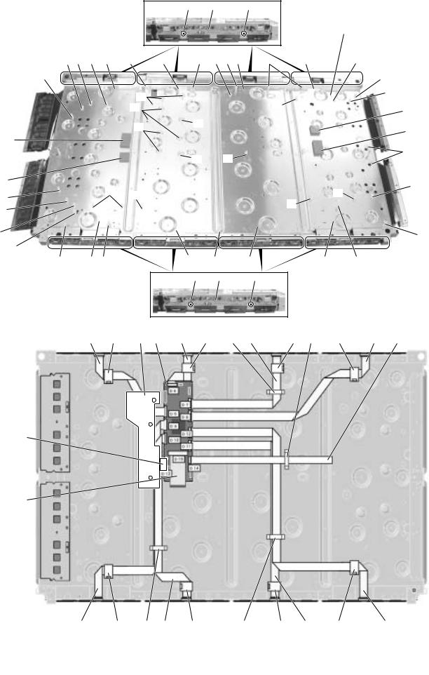
2.3 CHASSIS SECTION (2)
A
20
9
200V
20
2
17
|
|
17 |
B |
16 |
17 |
7 |
||
|
|
3 |
6 |
17 |
17 |
1 |
|
|||
18 |
|
|
|
|
18 |
17 |
|
|
|
|
16 |
|
|
|
17 |
|
|
17 |
|
4
C
8 |
5 |
 15
15
19 |
10 |
11 |
12 |
D
16
E
F
13 14
|
|
|
|
|
|
|
12 |
|
PDP-434PU |
|
|
||
1 |
2 |
|
|
|
3 |
4 |

5 6 7 8
CHASSIS SECTION (2) Parts list
Mark No. |
Description |
Part No. |
1 |
43 X DRIVE Assy |
AWZ6794 |
2 |
43 Y DRIVE Assy |
AWV2022 |
> 3 |
POWER SUPPLY Unit |
AXY1068 |
NSP 4 |
X CONNECTOR A Assy |
AWZ6798 |
NSP 5 |
X CONNECTOR B Assy |
AWZ6799 |
NSP 6 |
43 SCAN A Assy |
AWZ6796 |
NSP 7 |
43 SCAN B Assy |
AWZ6797 |
8 |
KEY CONTROL Assy |
AWZ6789 |
9 |
PANEL SENSOR Assy |
AWZ6795 |
10 |
3P Housing Wire (J109) |
ADX2847 |
11 |
11P Housing Wire (J102) |
ADX2840 |
12 |
12P Housing Wire(J103) |
ADX2841 |
13 |
3P Housing Wire (J108) |
ADX2846 |
14 |
Wire B (J106) |
ADX2844 |
15 |
Screw |
ABZ30P060FMC |
16 |
Screw |
PMB30P060FNI |
17 |
Screw |
VBB30P080FNI |
18 |
Screw |
PMB40P080FZK |
19 |
Wire A (J101) |
ADX2839 |
20 |
Nyron Rivet |
AEC1671 |
A
B
C
D
E
F
|
|
|
|
|
|
|
|
|
PDP |
-434PU |
7 |
13 |
|
5 |
6 |
|
|
|
8 |
|
|
1 |
2 |
3 |
4 |
|
|
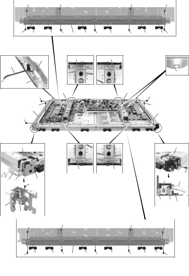
2.4 FLAME SECTION |
|
|
|
|
|
|
|
|
|
|
A |
17 |
19 |
19 |
17 |
|
|
|
|
|
|
|
17 |
11 |
11 |
18 |
10 |
11 |
18 |
11 |
18 |
11 |
11 |
17 |
B |
|
|
14 |
19 |
19 |
|
|
|
4 |
|
|
|
|
14 |
3 |
|
|
|
12 |
13 |
17 |
|
17 |
C |
|
17 |
17 |
|
|
15 |
|
16 |
|
|
|
17 |
|
|
23 |
21 |
D
|
|
|
19 |
|
19 |
|
|
|
|
|
|
2 |
17 |
||
22 |
8 |
9 |
|
5 |
|||
|
|
|
|
||||
20 |
|
|
|
|
|
||
|
|
|
|
|
|
|
|
E |
|
18 |
18 |
|
|||
7 |
|
|
|
|
6 |
||
|
|
|
|
|
|
||
1 |
|
|
|
|
|
||
|
|
|
|
|
|
|
|
17 |
19 |
19 |
|
17 |
|
||
|
|
|
|
||||
F |
11 |
11 |
|
|
11 |
|
11 |
|
11 |
11 |
|
17 |
18 |
10 |
18 |
18 |
17 |
|
|
|
|
|
|
|
14 |
|
PDP-434PU |
|
|
||
1 |
2 |
|
|
|
3 |
4 |

5 6 7 8
FLAME SECTION Parts list
Mark No. |
Description |
Part No. |
|
|
1 |
PANEL IR Assy |
AWZ6790 |
> |
2 |
Power Switch (S1) |
ASG1092 |
|
3 |
Power Switch (S2) |
ASG1089 |
|
4 |
3P Housing Wire (J107) |
ADX2845 |
|
5 |
Housing Wire (43) (J110) |
ADX2848 |
|
6 |
Switch Holder |
AMR3349 |
NSP |
7 |
IR Holder |
ANG2551 |
|
8 |
Wire Saddle |
AEC1948 |
|
9 |
Nyron Rivet |
AEC1671 |
NSP 10 |
Front Chassis H (43) |
ANA1714 |
|
|
11 |
Front Spacer |
AMR3369 |
|
12 |
Sub Frame L Assy (43P) |
ANG2545 |
|
13 |
Sub Frame R Assy (43P) |
ANG2548 |
|
14 |
Edging Saddle |
AEC1737 |
|
15 |
Front Chassis VL Assy (43) |
ANA1762 |
|
16 |
Front Chassis VR Assy (43) |
ANA1763 |
|
17 |
Screw |
AMZ30P060FZK |
|
18 |
Screw |
APZ30P080FZK |
|
19 |
Screw |
AMZ30P080FMC |
|
20 |
Screw |
ABZ30P060FMC |
|
21 |
Flat Clamp |
AEC1884 |
|
22 |
Flexible Cable (J211) |
ADD1225 |
|
23 |
Flat Clamp |
AEC1879 |
A
B
C
D
E
F
|
|
|
|
|
|
|
|
|
PDP |
-434PU |
7 |
15 |
|
5 |
6 |
|
|
|
8 |
|
1 |
2 |
3 |
4 |
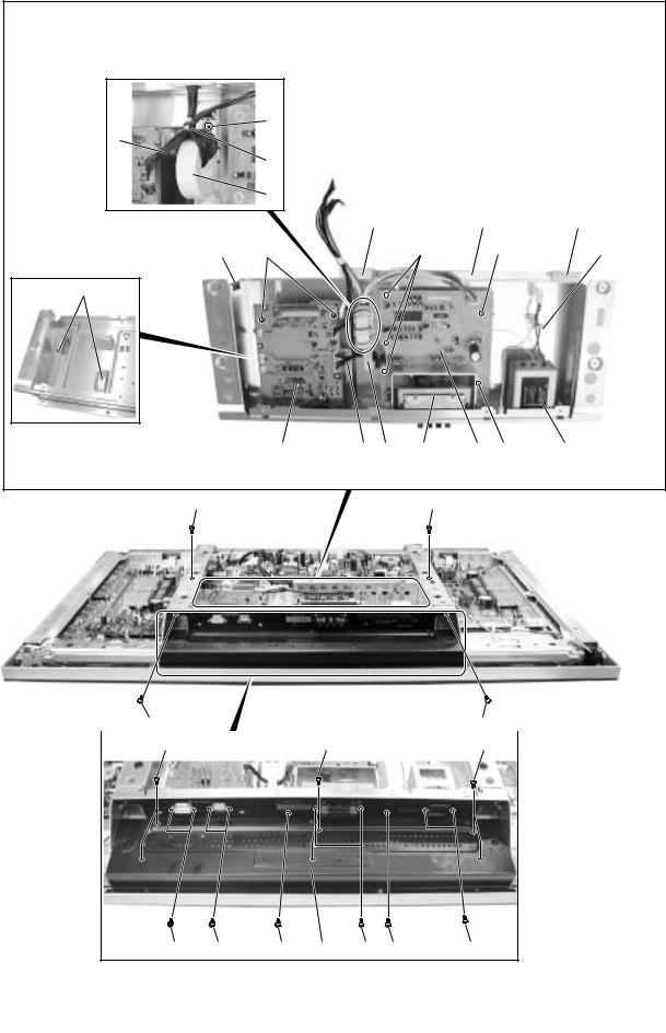
2.5 MULTI BASE SECTION
A |
|
|
|
|
|
|
|
|
19 |
|
|
|
|
|
|
6 |
|
|
|
|
|
|
|
|
16 |
|
|
|
|
|
|
B |
|
|
|
|
|
|
|
|
5 |
|
|
|
|
|
|
|
|
13 |
|
|
10 |
|
13 |
12 |
18 |
|
|
14 |
|
14 |
15 |
11 |
|
|
|
|
|
|
|
C |
|
|
|
|
|
|
|
|
1 |
9 |
13 |
3 |
2 |
14 |
4 |
17 |
|
|
|
|
17 |
|
|
D |
|
|
|
|
|
|
|
|
17 |
|
17 |
E |
17 |
17 |
17 |
|
|
|
F
20 21 17 23 22 17 17
|
|
|
|
|
|
|
16 |
|
PDP-434PU |
|
|
||
1 |
2 |
|
|
|
3 |
4 |

5 6 7 8
MULTI BASE SECTION Parts list
Mark No. |
Description |
Part No. |
|
|
1 |
PANEL IF Assy |
AWZ6786 |
A |
|
2 |
HD AUDIO AMP Assy |
AWZ6834 |
||
|
||||
3 |
HD SP TERMINAL Assy |
AWZ6792 |
|
|
> 4 |
AC Inlet |
AKP1244 |
|
|
5 |
Toroidal Core |
ATX1042 |
|
|
6 |
Wire C (J104) |
ADX2879 |
|
7• • • • •
8• • • • •
9 |
13P Housing Wire (J105) |
ADX2843 |
|
10 |
Multi Base Assy (P) |
ANA1718 |
|
|
|
|
B |
11 |
Locking Card Spacer |
AEC1940 |
|
12 |
Edge Saddle |
AEC1946 |
|
13 |
Clamp |
AEC1884 |
|
14 |
PCB Spacer |
AEC1941 |
|
15 |
Niplocker |
BEC1136 |
|
16 |
Nyron Binder |
AEC-093 |
|
17 |
Screw |
AMZ30P060FZK |
|
18 |
Screw |
PMB30P060FNI |
|
19 |
Screw |
ABA1294 |
|
20 |
Hexagon Head Screw |
BBA1051 |
C |
21 |
Screw |
PMZ26P060FZK |
|
22 |
Screw |
APZ30P080FZK |
|
23 |
Under Cover Assy |
ANG2589 |
|
D
E
F
|
|
|
|
|
|
|
|
|
PDP |
-434PU |
7 |
17 |
|
5 |
6 |
|
|
|
8 |
|

|
1 |
|
2 |
|
3 |
|
|
4 |
2.6 REAR SECTION |
|
|
|
|
|
|
|
|
A |
|
|
|
|
|
|
|
|
|
|
|
3 |
1 |
4 |
|
|
|
8 |
8 |
8 |
9 |
|
8 |
9 |
8 |
8 |
|
|
|
|
|
|
|||
9 |
|
|
|
|
|
|
|
8 |
|
|
|
|
|
|
|
|
|
|
|
|
|
|
|
|
|
9 |
7 |
|
|
|
|
|
|
|
7 |
B |
|
|
|
|
|
|
|
|
|
|
|
|
|
|
|
|
|
2 |
|
|
|
|
|
|
|
|
|
|
|
|
|
|
|
|
2 |
7 |
|
|
|
|
|
|
|
7 |
|
|
|
|
|
|
|
|
|
9 |
|
|
|
|
|
|
|
9 |
8 |
|
|
|
|
|
|
|
8 |
8 |
|
|
|
|
|
|
|
8 |
|
|
|
|
|
|
|
|
|
C |
|
|
|
|
|
|
|
|
9
9 |
8 |
8 |
9 |
9 |
8 |
8 |
5 |
9 |
8 |
8 |
9 |
9 |
8 |
8 |
8 |
|
D
E
F
|
|
|
|
|
|
|
18 |
|
PDP-434PU |
|
|
||
1 |
2 |
|
|
|
3 |
4 |

5 |
6 |
7 |
8 |
REAR SECTION Parts list
Mark No. |
Description |
Part No. |
1 |
Rear Case (43p) |
ANE1612 |
2 |
Grip |
AMR3380 |
NSP 3 |
Name Label |
See Contrast table (2) |
4 |
Caution Label |
See Contrast table (2) |
5 |
Terminal Label |
See Contrast table (2) |
6 |
• • • • • |
|
Mark No. |
Description |
Part No. |
7 |
Screw |
PMB50P120FZK |
8 |
Screw |
AMZ30P060FZK |
9 |
Screw |
ABZ30P100FZK |
(2) CONTRAST TABLE
PDP-434PU/ TUCK, PDP-434PE/ WYVI6, PDP-434PE/ WYVI6XK and PRO-434PU/ KUC are constructed the same except for the following :
Mark |
No. |
|
Symbol and Description |
PDP-434PU |
PDP-434PE |
PDP-434PE |
PRO-434PU |
|
TUCK |
WYVI6 |
WYVI6XK |
KUC |
|||
|
|
|
|
||||
|
|
|
|
|
|
|
|
NSP |
3 |
Name Label |
|
AAL2467 |
AAL2471 |
AAL2480 |
AAL2482 |
|
4 |
Caution Label |
|
AAX3007 |
AAX3007 |
AAX3005 |
AAX3007 |
|
5 |
Terminal Label |
|
AAX2997 |
AAX2998 |
AAX3006 |
AAX2997 |
|
|
|
|
|
|
|
|
A
B
C
D
E
F
|
|
|
|
|
|
|
|
|
PDP |
-434PU |
7 |
19 |
|
5 |
6 |
|
|
|
8 |
|
1 |
2 |
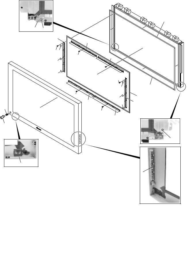
2.7 FRONT PANEL SECTION
A
1 12
6
6
B |
13 7 |
|
15
7
8  7
7
|
15 |
C |
6 |
|
|
|
10 |
|
9 |
D
11
• Rear side
E
F
3
3 
6
15 

13
7
7
7
15
6
4
4
 3
3
4
5
6
13
2 
|
|
|
|
|
|
|
20 |
|
PDP-434PU |
|
|
||
1 |
2 |
|
|
|
3 |
4 |
5 6 7 8
FRONT PANEL SECTION Parts list
Mark No. |
Description |
Part No. |
Mark No. |
Description |
Part No. |
1 |
PANEL LED Assy |
AWZ6787 |
9 |
Power Button |
See Contrast table (2) |
2 |
PANEL KEY Assy |
AWZ6788 |
10 |
Coil Spring |
ABH1114 |
3 |
Panel Cushion V (43) |
AED1201 |
11 |
Blind Cushion |
AEB1383 |
4 |
Panel Cushion H (43) |
AED1200 |
12 |
Screw |
BBZ30P050FMC |
5 |
Protect Panel Assy 43 |
See Contrast table (2) |
13 |
Screw |
ABZ30P060FMC |
NSP 6 |
Panel Holder (43) |
ANG2552 |
14 |
Serial Sheet |
AAX2609 |
7 |
Cushion |
AEB1393 |
15 |
Screw |
APZ30P080FZK |
8 |
Front Case Assy |
See Contrast table (2) |
|
|
|
(2) CONTRAST TABLE
PDP-434PU/ TUCK, PDP-434PE/ WYVI6, PDP-434PE/ WYVI6XK and PRO-434PU/ KUC are constructed the same except for the following :
Mark |
No. |
Symbol and Description |
PDP-434PU |
PDP-434PE |
PDP-434PE |
PRO-434PU |
|
TUCK |
WYVI6 |
WYVI6XK |
KUC |
||||
|
|
|
|||||
|
|
|
|
|
|
|
|
|
5 |
Protect Panel Assy (43) |
AMR3383 |
AMR3345 |
AMR3345 |
AMR3345 |
|
|
8 |
Front Case Assy |
AMB2779 |
AMB2779 |
AMB2779 |
AMB2783 |
|
|
9 |
Power Button |
AAD4123 |
AAD4123 |
AAD4123 |
AAD4126 |
|
|
|
|
|
|
|
|
2.8 PDP SERVICE Assy (AWU1079)
PDP SERVICE Assy (AWU1079) Parts list
Mark No. |
Description |
Part No. |
NSP |
1..P. Chassis (43) Assy |
AWU1070 |
NSP |
2..Front Chassis H (43) |
ANA1714 |
|
2..Front Chassis VL (43) |
ANA1762 |
|
2..Front Chassis VR (43) |
ANA1763 |
|
2..Sub Frame L Assy |
ANG2545 |
|
2..Sub Frame R Assy |
ANG2548 |
|
2..Wire Saddle |
AEC1745 |
|
2..Clamp |
AEC1884 |
|
2..PCB Support |
AEC1938 |
|
2..PCB Spacer |
AEC1941 |
|
2..PCB Spacer |
AEC1947 |
|
2..Wire Clip |
AEC1948 |
|
2..Ferrite Clamp (Plastic) |
AEC1972 |
|
2..Panel Cushion H (43) |
AED1200 |
|
2..Panel Cushion V (43) |
AED1201 |
|
2..Ydrive Protect Sheet |
AMR3346 |
Mark No. |
Description |
Part No. |
|
2..Front Spacer |
AMR3369 |
|
2..Caution Label |
AAX3031 |
|
2..Spacer |
AEB1397 |
|
2..Edging Saddle |
AEC1737 |
NSP |
2..Drive Voltage Label |
ARW1097 |
|
2..Front Case (434 Service) |
AMB2810 (Note) |
|
2..Rear Case (43P) |
ANE1612 (Note) |
Note: The front case (434 Service) and rear case (434p) attached to the Service Assy are for transportation only.
Do NOT use them as parts of the unit.
2..Screw |
AMZ30P060FZK |
2..Screw |
AMZ30P080FMC |
2..Screw |
AMZ30P080FZK |
2..Screw |
PMB30P060FNI |
2..Screw |
VBB30P080FNI |
2..Screw |
ABZ30P100FZK |
A
B
C
D
2.9 PANEL CHASSIS (43) Assy (AWU1070)
PANEL CHASSIS (43) Assy (AWU1070) Parts list
Mark No. |
Description |
Part No. |
NSP |
1..43 ADDRESS Assy |
AWV2020 |
NSP |
2..43 ADDRESS Assy |
AWZ6793 |
NSP |
1..43 SCAN FUKUGO Assy |
AWV2023 |
NSP |
2..43 SCAN A Assy |
AWZ6796 |
NSP |
2..43 SCAN B Assy |
AWZ6797 |
NSP |
2..X CONNECTOR A Assy |
AWZ6798 |
NSP |
2..X CONNECTOR B Assy |
AWZ6799 |
NSP |
1..Address Module (IC1-IC32) |
AXF1115 |
NSP |
1..Plasma Panel Assy (43")(V1) |
AAV1243 |
NSP |
1..FPC (43XGA-X) |
ADY1079 |
NSP |
1..FPC (43XGA-Y) |
ADY1080 |
NSP |
1..Chassis Assy (43) |
ANA1733 |
|
5 |
6 |
Mark No. |
Description |
Part No. |
|
1..PCB Spacer |
AEC1944 |
|
1..PCB Support |
AEC1958 |
|
1..Rivet (Plastic) |
AMR1066 |
|
1..FC Spacer |
AMR3370 |
|
1..Adhesive |
ZBA-KE3424G |
NSP |
1..Lotion |
ZLX-AP7 |
NSP |
1..Tape |
ZTA-8101-12 |
NSP |
1..Double Faced Tape |
ZTB-5015-18 |
NSP |
1..Tape |
ZTC-POLYCA-11 |
NSP |
1..Tape |
ZTC-POLYCA-20 |
NSP |
1..Tape |
ZTC-900UL-15 |
NSP |
1..Silicone Rubber |
ZTX-HC20-15 |
NSP |
1..Wiping Cloth |
ZTX-MX100-13 |
NSP |
1..Film |
ZTX-2102Y35-2R5 |
NSP |
1..Film |
ZTX-2102Y45-5 |
|
|
|
|
|
PDP |
-434PU |
7 |
21 |
|
|
|
|
8 |
|
E
F
A
B
C
D
E
1 |
2 |
3 |
4 |
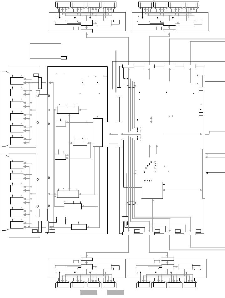
3. BLOCK DIAGRAM AND SCHEMATIC DIAGRAM
3.1 BLOCK DIAGRAM
3.1.1 OVERALL BLOCK DIAGRAM
DRIVER IC |
DRIVER IC |
DRIVER IC |
DRIVER IC |
DRIVER IC |
DRIVER IC |
DRIVER IC |
DRIVER IC |
||
IC1552 |
IC1553 |
|
IC1554 |
IC1555 |
IC1552 |
IC1553 |
|
IC1554 |
IC1555 |
V+5V |
|
|
|
|
V+5V |
|
|
|
|
V+3V_LVDS V+3V_PLL V+3V_IC5 |
|
|
V+9V V+60V |
V+3V_LVDS V+3V_PLL V+3V_IC5 |
|
|
V+9V V+60V |
||
|
V+ADR |
|
V+ADR |
||||||
|
IC1501 |
RESONANCE |
|
IC1501 |
RESONANCE |
||||
|
|
BLOCK |
|
|
BLOCK |
||||
|
|
|
|
|
|
|
|
||
|
AD1 |
|
43 ADDRESS ASSY |
|
AD1 |
|
43 ADDRESS ASSY |
||
|
CN1501 |
|
|
CN1501 |
|
||||
PANEL SENSOR ASSY
|
|
CN1071 |
|
SENSOR |
|
||
IC1072 |
|
|
|
|
|
|
|
|
|
|
|
TE1
CN5501 |
CN5502 |
CN5503 |
CN5504 |
43 SCAN B ASSY
IC5V |
VCC |
SB1 |
|
_VH |
|
||
ADD |
PSUS |
CN3201 |
|
VCC |
|
||
SEL_PULSE |
SCAN |
||
IC3201 |
|
|
|
IC5V |
_VH |
|
|
|
|
|
|
ADD |
|
|
|
SEL_PULSE |
|
|
|
IC3202 |
|
|
|
VCC
IC5V _VH
ADD
SEL_PULSE
IC3203
VCC
IC5V _VH
ADD
SEL_PULSE
IC3204
VCC
IC5V _VH
ADD
SEL_PULSE
IC3205
VCC
IC5V _VH
ADD
SEL_PULSE
IC3206
VCC
 IC5V
IC5V  _VH
_VH
PSUS
ADD
SEL_PULSE
IC3001
VCC
IC5V _VH
ADD
SEL_PULSE
IC3002
VCC
IC5V _VH
ADD
SEL_PULSE
IC3003
VCC
IC5V _VH
ADD
SEL_PULSE
IC3004
VCC
IC5V _VH
ADD
SEL_PULSE
IC3005
IC5V |
VCC |
|
_VH |
|
|
|
|
|
ADD |
|
CN3001 |
SEL_PULSE |
SCAN |
|
IC3006 |
|
|
|
SA1 |
|
43 SCAN A ASSY
|
VCC_VH V_IC5V |
43 Y DRIVE ASSY |
|
|
|
|
|
|||||||||||||||
|
|
|
|
|
|
|
VCC_VH V_IC5V |
|
|
|
|
|
||||||||||
|
Y2 |
|
|
|
|
|
|
|
|
|
|
|||||||||||
|
|
|
|
|
|
|
|
|
|
|
|
|
|
|
|
|
Y4 |
|
|
|
|
|
CN2101 |
|
|
|
|
V_OFS |
|
|
DC_DC |
|
|
|
|
|
|
|
|
CN5202 |
|||||
|
|
|
|
|
|
|
VSUS |
CN2301 |
|
|
|
|||||||||||
|
|
|
|
|
VC_VF- |
|
|
|
CONV |
|
|
|
|
|
|
|||||||
|
|
|
|
|
|
|
|
|
|
|
|
|
|
|
|
|
||||||
|
|
|
|
|
VC_VF+ |
|
|
BLOCK |
|
|
+6.5V |
|
|
|
|
|
||||||
|
|
|
|
|
|
|
|
|
|
|
|
|
|
|
|
|
|
|
||||
|
|
|
|
|
|
|
|
|
|
|
|
|
|
|
|
|
|
|
|
|
||
|
|
|
|
|
|
|
|
|
|
|
|
|
|
|
|
|
|
|
|
|
||
|
|
|
|
|
|
|
|
|
|
|
|
|
|
|
|
|
|
|
|
|
||
|
|
|
|
|
+5V |
|
|
REGULATOR |
|
|
|
|
|
|
|
|
||||||
|
|
|
|
|
|
|
|
|
|
|
|
|
|
|
|
|
|
|
|
|
|
|
|
|
|
|
|
|
|
|
|
|
|
|
|
|
|
|
|
|
|
|
|
|
|
PSUS
+5V +16.5V VSUS
MASK MOD
IC2307
+16.5V
Drive
Signal
SOFT-D
BLOCK 
+5V +16.5V
RESONANCE
BLOCK
+16.5V  VSUS
VSUS
Drive
+RESET Signal
BLOCK
+5V
LOGIC BLOCK
Y1  CN2001
SCAN |
CN5521 |
|
YSUS |
||
|
VH_UV_PD
YDRIVE_P DYRESNC_PD YDD_CHV_PD IC5V_UV_PD
ADR_ |
|
|
|
D5 |
|
|
|
|
D6 |
|
|
|
|
D7 |
|
|
|
|
D8 |
|
|
|
|||||
|
|
|
ADR_PD1 |
|
|
|
|
|
|
|
|
|
|
|
|
|
|
|
|
|
|||||||
|
PD0 |
|
|
|
|
ADR_PD2 |
|
|
|
|
|
|
V+60V |
|
|
||||||||||||
|
|
|
|
|
|
|
|
|
|
|
|
|
|
|
|
|
|
ADR_PD3 |
|
|
|
|
|
|
CN5602 |
||
|
|
|
|
|
|
|
|
|
|
|
|
|
|
|
|
|
|
|
|
|
|
V+6.5V |
|
||||
OR |
|
|
|
|
|
|
|
|
|
|
|
|
|
|
|
|
|
|
|||||||||
|
|
|
|
|
|
|
|
|
|
|
|
|
|
|
|
|
|
|
|||||||||
|
|
|
|
|
|
|
|
|
|
|
|
|
LVDS |
|
|
|
DIGITAL VIDEO ASSY |
|
|
|
|
|
|
|
|||||||||||||||||||||||
|
|
|
|
|
|
|
|
|
|
|
|
|
|
|
|
|
|
|
|
||||||||||||||||||||||||||||
|
|
|
|
|
|
|
|
|
|
|
|
|
|
|
|
|
|
||||||||||||||||||||||||||||||
|
|
|
|
|
|
|
|
|
|
|
|
V+3V_D |
|
|
|
|
|
|
|
|
|
V+12V |
|
|
|
|
|
|
D2 |
|
|
|
|||||||||||||||
|
|
|
|
|
|
|
|
|
|
|
|
|
|
|
|
|
|
|
|
|
|
|
V+12V |
|
|
|
|||||||||||||||||||||
|
|
|
|
|
|
|
|
|
|
|
|
|
|
|
|
|
|
|
|
|
|
|
|
|
|
|
|
|
|
|
|
|
|
|
|
|
|
|
|
|
|||||||
|
|
|
|
|
|
|
|
|
|
|
|
|
|
|
|
|
|
|
|
|
|
DC-DC |
|
|
|
|
|
|
|
|
|
|
|
|
|
|
|
|
|
|
|
|
|||||
|
|
|
|
|
|
|
|
|
|
|
V+1V_D |
|
CONVERTER |
|
|
|
|
|
|
|
|
|
|
Vsus_ADJ. |
|
|
|
|
|||||||||||||||||||
|
D4 |
|
|
|
|
|
|
|
|
|
|
|
|
|
|
|
|
MODULE |
|
|
|
|
|
|
|
|
|
|
PD_PWDN |
CN5601 |
|
||||||||||||||||
|
|
|
|
|
|
|
|
|
|
|
|
|
|
|
|
|
|
|
|
|
AXY1066 |
|
|
|
|
|
|
|
|
|
|
|
|
|
|||||||||||||
|
|
|
|
|
|
|
|
|
|
|
DCC_PD |
|
|
|
|
|
|
|
|
|
|
|
|
|
|
|
|
|
|
|
|
|
|
||||||||||||||
|
|
|
|
|
|
|
|
|
|
|
|
|
|
|
|
|
|
|
|
|
|
|
|
|
|
|
|
|
|
|
|
|
|
|
|
|
|
|
|
|
|
|
|
|
|
|
|
|
|
|
|
|
|
|
|
|
|
|
|
|
|
|
|
|
|
|
|
|
|
|
|
|
|
|
|
|
|
|
|
|
|
|
|
|
|
|
|
|
|
|
|
|
|
|
|
|
|
|
|
|
|
|
|
|
|
|
|
|
|
|
|
|
|
FLASH MEMORY |
|
|
|
|
|
OR |
|
|
|
|
|
|
|
D1 |
|
|
|
||||||||||||
|
|
|
|
|
|
|
|
|
|
|
|
|
|
|
|
|
|
|
|
|
IC5305 |
|
|
|
|
|
|
|
|
|
|
|
|
|
|
|
|
|
|
||||||||
|
|
|
|
|
|
|
|
|
|
|
|
|
|
|
|
|
|
|
|
|
|
|
|
|
|
|
|
|
|
|
|
|
|
|
|
|
|
|
|
|
|
||||||
|
|
|
|
|
|
|
|
|
|
|
|
|
|
|
|
|
|
|
|
|
|
|
|
|
|
|
|
|
|
|
|
|
|
|
|
|
|
|
|
|
|
|
|
|
|
|
|
|
D13 |
|
|
|
|
|
|
|
|
|
|
|
|
|
|
|
|
|
|
|
|
|
|
|
|
|
|
|
|
|
|
|
|
|
|
|
|
|
|
|
|
|
|
|
|||
|
|
|
|
|
|
|
|
|
|
|
|
|
|
|
|
|
|
|
|
|
|
|
|
|
|
|
|
|
|
|
|
|
|
|
|
|
|
|
|
|
|
|
|
||||
|
|
|
|
|
|
|
|
|
|
|
|
|
|
|
|
|
|
|
|
|
|
|
|
|
|
|
|
|
|
|
|
|
|
|
|
|
|
|
|
|
|
|
|
|
|
|
|
|
|
|
|
|
|
|
|
|
|
|
|
|
|
|
|
|
|
|
|
|
|
|
|
|
|
|
|
|
|
|
|
|
|
|
|
|
|
|
|
|
|
|
|
|
|
|
|
|
|
|
|
|
|
|
|
|
|
|
|
|
|
|
|
|
|
SUB-FILD CONV. |
|
|
|
|
|
|
|
|
|
|
|
|
|
D14 |
|
|
|
||||||||||||
|
|
|
|
|
|
|
|
|
|
|
|
|
|
|
|
|
|
|
|
|
|
|
|
|
|
|
|
|
|
|
|
|
|
|
|
|
|
||||||||||
|
|
|
|
|
|
|
|
|
|
|
|
|
|
|
|
|
|
|
|
|
|
|
|
|
|
|
|
|
|
|
|
|
|
|
|
|
|||||||||||
|
|
|
|
|
|
|
|
|
|
|
|
|
|
|
|
|
|
|
& |
|
|
|
|
|
|
|
|
|
|
|
|
|
|
|
|
|
|
|
|
|
|
|
|
||||
|
|
|
|
|
|
|
|
|
|
|
|
|
|
|
|
|
XY DRV SEQUENCE |
|
|
|
|
|
|
|
|
|
|
XSUS |
CN5511 |
|
|||||||||||||||||
|
|
|
|
|
|
|
|
|
|
|
|
|
|
|
|
|
|
|
|
|
IC5401 |
|
|
|
|
|
|
|
|
|
|
|
|
|
|
|
|
|
|
||||||||
|
|
|
|
|
|
|
|
|
|
|
|
|
|
|
|
|
|
|
PATTERN GEN. |
|
|
|
|
|
|
|
|
|
|
|
|
|
|
|
|
|
|
|
|
||||||||
|
|
|
|
|
|
|
|
|
|
|
|
|
|
|
|
|
|
|
|
PD5856A |
|
|
|
|
|
|
|
|
|
|
|
|
|
|
|
|
|
|
|
|
|||||||
|
|
|
|
|
|
|
|
|
|
|
|
|
|
|
|
|
|
|
|
|
|
|
|
|
|
|
|
|
|
|
|
|
|
|
|
|
|
XSUSTN_PD |
|
|
|
||||||
|
|
|
|
|
|
|
|
|
|
|
|
|
|
|
|
|
|
|
|
|
|
|
|
|
|
|
|
|
|
|
|
|
|
|
|
|
|
XDD_CNV_PD |
|
|
|
||||||
|
|
|
|
|
|
|
|
|
|
|
|
|
|
|
|
|
|
|
|
|
|
|
|
|
|
|
|
|
|
|
|
|
|
|
|
|
|
XDRIVE_PD |
|
|
|
||||||
|
|
|
|
|
|
|
|
|
|
|
|
|
|
|
|
|
|
|
|
|
|
|
|
|
|
|
|
|
|
|
|
|
|
|
|
|
|
DCLK, DE |
|
|
|
||||||
|
|
|
|
|
|
|
|
|
|
|
|
|
|
|
|
|
|
|
|
|
|
|
|
|
|
|
|
|
|
|
|
|
|
|
|
|
|
HD, VD |
|
|
|
||||||
|
|
|
|
|
|
|
|
|
|
|
|
|
|
|
|
|
|
|
|
|
|
|
|
|
|
|
|
|
|
|
|
|
|
|
|
|
|
|
|
|
|
|
|
|
|
|
|
|
|
|
|
|
|
|
|
|
|
|
|
|
|
|
|
|
|
|
|
|
|
|
|
|
|
|
|
|
|
|
|
|
|
|
|
RA IN, GA IN, BA IN |
|
|
|
||||||||
|
|
|
|
|
|
|
|
|
|
|
|
|
|
|
|
|
|
|
|
|
|
|
|
|
|
|
|
|
|
|
|
|
|
|
|
RB IN, GB IN, BB IN |
|
|
|
||||||||
|
|
|
|
|
|
|
|
|
|
|
|
|
|
|
|
|
|
|
|
|
|
|
|
|
OR |
|
|
|
|
|
|
|
|
|
|
|
|||||||||||
|
|
|
|
|
|
|
|
|
|
|
|
|
|
|
|
|
|
|
|
|
|
|
|
|
|
|
|
|
|
|
|
|
|
|
|
|
|
|
|
|
|
|
|
|
|||
|
|
|
|
|
|
|
|
|
|
|
|
|
|
|
|
|
|
|
|
|
|
|
|
|
|
|
|
|
|
|
|
|
|
|
|
|
|
|
|
|
|
|
|
|
|||
|
|
|
|
|
|
|
|
|
|
|
|
|
|
|
|
|
|
|
|
|
|
|
|
|
|
|
|
|
|
|
|
|
PD |
|
|
|
|
|
|
|
|
|
|
CN5001 |
|
||
|
|
|
|
|
|
|
|
|
|
|
|
|
|
|
|
|
|
|
|
|
|
|
|
|
|
|
|
|
|
|
|
|
|
|
|
|
|
|
|
|
|
|
|
|
|
|
|
|
|
|
|
|
|
|
|
|
|
|
|
|
MASK |
|
|
|
|
|
|
|
|
|
|
|
|
|
|
|
|
|
|
|
|
|
|
D15 |
|
|
|
|
|
||||||
|
|
|
|
|
|
|
|
|
|
|
|
|
|
|
|
|
|
|
|
|
|
|
|
|
|
|
|
|
|
|
|
|
|
|
|
|
|
|
|
|
|
|
|
|
|
|
|
|
|
|
|
|
|
|
|
|
|
|
|
|
|
|
|
|
|
|
|
|
|
|
|
|
|
|
|
|
|
|
|
|
|
|
|
|
|
|
|
|
|
|
|
|
|
|
|
|
|
|
|
|
|
|
|
|
|
|
|
|
|
|
|
|
|
|
|
|
|
|
|
|
|
|
|
|
|
|
|
|
|
|
|
|
|
|
|
|
|
|
|
|
|
||
|
|
|
|
|
|
|
|
|
|
|
|
|
|
|
|
|
|
|
|
|
|
|
|
|
|
|
|
PD_MUTE |
|
|
|
|
|
|
|
|
|
|
|
|
|||||||
|
|
|
|
|
|
|
|
|
|
|
|
|
|
|
|
|
|
|
|
|
|
|
|
|
|
|
|
|
|
|
|
|
|
|
|
|
|
|
|
|
|
|
|
|
|
|
|
PSUS |
+5V +16.5V |
VSUS |
Vofs |
RELAY, PD_TRIGGER |
|
|
|
IC5201 |
|
|
|
|
Drive |
MODULE UCOM |
|
MASK MOD |
Signal |
|
|
|
|
|
||
|
IC2303 |
|
|
|
|
VC_VF+ VC_VFV_OFS |
|
|
|
|
|
OFFSET |
LVDS |
PSIZE |
|
|
|
|
|
|
|
BLOCK |
|
|
|
V_IC5V VCC_VH |
|
|
|
|
|
|
|
|
V_IC5V |
OR |
|
|
|
|
CN2102 |
|
|
|
|
|
|
|
|
Photo Coupler |
|
|
ADR_PD6 |
ADR_PD7 |
|
|
|
Scan Signal |
BLOCK |
ADR_ |
ADR_PD5 |
|
|
|
|
|
|
|
||||
|
Y3 |
|
PD4 |
D9 |
D10 |
D11 |
D12 |
|
|
|
CN5505 |
CN5506 |
CN5507 |
|
CN5508 |
|
|
CN1501 |
|
|
CN1501 |
|
||||
|
|
AD1 |
|
43 ADDRESS ASSY |
|
AD1 |
|
43 ADDRESS ASSY |
||
|
|
IC1501 |
RESONANCE |
|
IC1501 |
RESONANCE |
||||
|
|
|
BLOCK |
|
|
BLOCK |
||||
F |
|
|
|
|
|
|
|
|
||
V+3V_LVDS V+3V_PLL |
V+3V_IC5 |
|
V+ADR |
V+3V_LVDS V+3V_PLL |
V+3V_IC5 |
|
V+ADR |
|||
|
|
|
|
|
V+9V V+60V |
|
|
|
|
V+9V V+60V |
|
V+5V |
|
|
|
|
V+5V |
|
|
|
|
|
DRIVER IC |
DRIVER IC |
DRIVER IC |
DRIVER IC |
DRIVER IC |
DRIVER IC |
DRIVER IC |
DRIVER IC |
||
|
IC1552 |
IC1553 |
|
IC1554 |
IC1555 |
IC1552 |
IC1553 |
|
IC1554 |
IC1555 |
|
22 |
|
|
PDP-434PU |
|
|
|
|
|
|
|
1 |
2 |
|
|
|
3 |
|
|
|
4 |
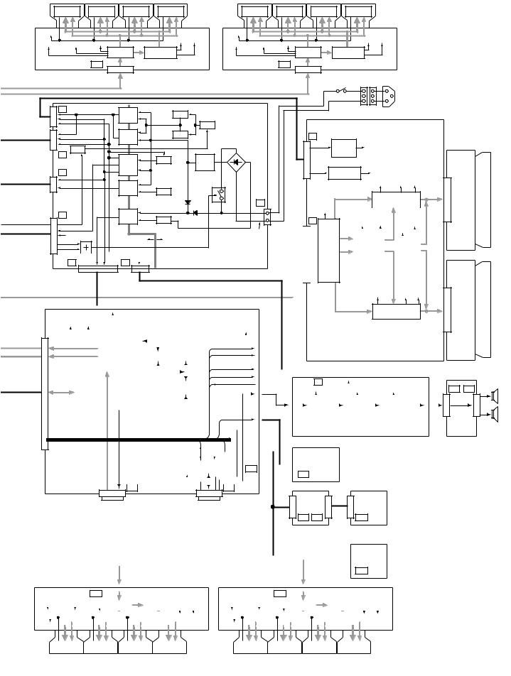
5 |
6 |
7 |
8 |
DRIVER IC |
DRIVER IC |
DRIVER IC |
DRIVER IC |
DRIVER IC |
DRIVER IC |
DRIVER IC |
DRIVER IC |
||
IC1552 |
IC1553 |
IC1554 |
IC1555 |
IC1552 |
IC1553 |
IC1554 |
IC1555 |
||
V+5V |
|
|
|
|
V+5V |
|
|
|
|
V+3V_LVDS V+3V_PLL V+3V_IC5 |
|
|
V+9V V+60V |
V+3V_LVDS V+3V_PLL V+3V_IC5 |
|
|
V+9V V+60V |
||
|
V+ADR |
|
V+ADR |
||||||
|
IC1501 |
RESONANCE |
|
IC1501 |
RESONANCE |
||||
|
|
BLOCK |
|
|
BLOCK |
||||
|
|
|
|
|
|
|
|
||
|
AD1 |
|
43 ADDRESS ASSY |
|
AD1 |
|
43 ADDRESS ASSY |
||
|
CN1501 |
|
|
|
CN1501 |
|
|
||
|
|
|
|
|
|
|
|
|
S1 |
|
|
|
|
|
|
|
|
MAIN POWER |
|
|
|
|
|
|
|
|
|
|
AC INLET |
|
|
|
|
|
|
|
LIVE |
|
|
P4 VSUS |
T105 |
|
Switching Q120 |
|
|
NEUTRAL |
|
||
|
|
|
|
M107 |
|
|
|
|
43 X DRIVE ASSY |
|
|
|
|
Switching Q119 |
|
|
|
|
|
|
+6.5V |
T103 |
|
|
|
X2 |
|
|
|
|
|
|
|
|
|
|
|||
+16.5V |
|
|
|
|
|
|
M111 |
VSUS_ |
|
|
|
|
RC101 |
P3 |
CONT |
|
|
+390V |
PFC |
|
|
|
Q116 |
|
|||
|
|
T101 |
Q101, |
|
||
|
|
Switching |
|
|||
P5 |
|
|
Q102 |
|
||
|
|
|
|
|
|
|
+6.5V |
|
|
|
|
|
|
VADR |
|
T102 |
|
|
RL101 |
|
|
|
Q117 |
|
|
|
|
|
|
|
|
|
|
|
|
|
|
Switching |
|
P7 |
|
|
|
|
|
D133 |
||
P2 |
|
|
|
|
|
LIVE |
|
T104 |
M105 |
D131,D134 |
|
||
Vsus_ADJ. |
|
|
|
|||
|
|
|
|
|
||
+12V |
|
|
Switching |
|
NEUTRAL |
|
PS.PD |
|
|
|
|
RELAY |
|
|
SECONDARY |
PRIMARY |
|
|||
EXT.PD |
|
& PD |
|
|||
RELAY |
|
|
|
|
|
|
|
|
|
|
|
|
|
|
|
STB |
+6.5V |
|
|
|
|
POWER SUPPLY UNIT |
|||||
|
|
|
|
|
|
|
|
||||||
|
P1 |
|
|
3.3V |
P6 |
|
|
|
|||||
|
|
|
|
|
|
|
|
|
|
|
|
||
|
|
|
|
|
|
|
|
|
|
|
|
|
|
|
|
|
|
|
|
|
|
|
|
|
|
|
|
|
VSUS |
DC_DC |
V_RN |
|
|
CONV |
|
CN1201 |
|
BLOCK |
|
+6.5V |
|
|
|
|
|
REGULATOR |
+5V |
VSUS +16.5V +5V
PSUS
MASK MOD
IC1203
+5V |
Drive |
SUS |
|
Signal |
|||
|
|||
|
|
OUT |
X1  CN1001
LOGIC BLOCK
+16.5V |
+5V |
|
|
+16.5V |
|||
|
|
|
|
V_RN |
|
||
|
|
|
|
|
|||
RESONANCE |
|
|
|
|
|||
|
|
|
|
||||
|
-RESET |
||||||
BLOCK |
|
||||||
|
PULSE |
||||||
|
|
|
|
|
BLOCK |
||
SUS
OUT
VSUS |
+16.5V +5V |
 CN4004
|
|
|
|
|
|
|
CN4001 |
|
|
|
|
|
|
|
|
|
|
|
|
|
|
|
|
|
||||
|
|
R1 |
|
V+3V |
|
|
|
|
|
|
PANEL IF ASSY |
|
|
|
|
|
|
|||||||||||
|
V+6.5V |
ACTV |
|
|
|
STB3.3 |
|
|
|
|
|
|
|
|
|
|
|
|
|
R7 |
|
|||||||
|
|
|
|
MUTE |
|
|
|
|
|
|
|
|
|
|
|
V+6.5V |
|
|||||||||||
|
|
|
|
|
|
|
|
|
|
|
|
|
|
|
|
|
|
|
|
|
|
|
|
|
|
|
|
|
R4 |
|
|
|
|
|
|
|
|
|
|
|
|
|
|
|
|
|
|
|
|
|
|
|
|
|
|
|
|
|
|
|
|
|
|
|
|
|
|
|
|
|
|
|
|
|
|
|
|
|
|
|
|
|
||||
|
|
DCLK, DE |
|
|
|
|
|
|
|
|
|
|
|
|
|
|
|
|
|
|
|
|
||||||
|
|
HD, VD |
TMDS RECEIVER |
|
|
|
|
|
|
|
|
|
|
A_SCL,A_SDA,SRS |
|
|||||||||||||
|
|
|
|
|
|
|
|
|
|
|
|
|
EEPROM |
|
|
FOCUS,TRUBASS |
CN4009 |
|||||||||||
RB IN, GB IN, BB IN |
|
IC4202 |
|
FET SW |
|
for EDID |
|
|
A_MUTE |
|||||||||||||||||||
RA IN, GA IN, BA IN |
|
|
|
|
|
|
|
|
|
|
|
|
|
|
ST_BY |
|
||||||||||||
|
|
|
|
|
|
|
|
|
|
|
|
|
|
|
|
|
|
|
|
|
|
|
|
|||||
|
|
|
|
|
|
|
|
|
|
|
|
|
|
|
|
|
|
|
|
|
|
|
|
|||||
|
|
|
|
|
|
|
|
|
|
|
|
|
|
|
|
|
|
|
|
|
|
|
A_NG |
|
||||
|
|
|
|
|
|
|
|
|
|
|
|
|
|
|
|
|
|
Bus |
|
|
|
|
|
|
|
|
||
|
|
|
|
|
EEPROM |
|
|
|
|
|
|
|
|
|
Buffer |
|
|
AUDIO L |
|
|
|
|
||||||
B_SDA |
for Backup |
|
|
|
|
|
|
|
|
|
|
|
|
|
|
|
|
|
|
|||||||||
|
|
|
|
|
|
|
|
|
|
|
|
|
|
|
AUDIO R |
|
||||||||||||
B_SCL |
|
|
|
|
|
|
|
|
|
|
|
|
|
|
|
|
|
|
|
|
||||||||
|
|
|
|
|
|
|
|
|
|
|
|
|
|
|
|
|
|
|
|
|
|
|
|
|
|
R6 |
|
|
|
|
|
|
|
|
|
|
|
|
|
|
|
|
|
|
|
|
|
|
|
|
|
LED_R,G |
CN4007 |
||||
|
|
|
|
|
|
|
|
|
|
|
|
|
|
|
|
|
|
|
|
|
|
|
|
|
|
|
|
|
|
|
|
|
|
|
|
|
|
|
|
|
|
|
|
|
|
|
|
|
|
|
|
|
|
|
|
|
|
|
|
|
|
|
|
|
|
|
|
|
|
|
|
|
|
|
|
|
|
|
|
|
|
|
|
|
|
|
Drive
Signal
MASK MOD
IC2303
PSUS
|
|
|
|
|
|
|
|
|
|
|
|
|
|
|
|
|
|
|
|
|
|
|
|
|
|
|
|
|
|
|
|
|
|
|
|
CN3504 |
|
|
+16.5V |
|
|
|
|
|
|
|
|
|
|
||||||
|
|
|
|
|
A4 |
|
|
|
|
|
|
|
|
|
|
|
|
||||||||||
|
|
A1 |
|
+9V |
|
|
|
|
|
+9V |
|
|
+16.5V |
|
A3 |
|
|
|
|||||||||
|
|
|
|
|
|
|
|
|
|
|
|
|
|
|
|
|
|
|
|
|
|
|
|
|
|
|
|
|
CN3501 |
L,R |
|
|
|
|
|
|
L,R |
|
|
|
|
L,R |
|
|
L,R |
CN3503 |
L,R |
||||||||
|
WOW IC |
|
VOL IC |
POWER AMP |
|||||||||||||||||||||||
|
|
|
|
IC3501 |
|
|
|
|
|
IC3502 |
|
|
IC3504 |
|
|
|
|
|
|
||||||||
|
|
|
|
|
|
|
|
|
|
|
|
|
|
|
|
|
|
|
|
|
|
|
|
|
|
|
|
HD AUDIO AMP ASSY
X CONNECTOR A ASSY
X CONNECTOR B ASSY
J3701 |
SP2 |
SP1 |
SPEAKER |
L,R |
CN3701 |
||
|
|
|
|
|
|
|
|
|
Buffer |
|
|
|
|
|
|
CN4010 |
|
|
|
|
|
|
LED |
||
|
|
|
V+3V_STB |
|
STB |
|
|
|
R8 |
|
|
|
CN4751 |
|
|
|||||||
|
|
|
|
|
|
|
|
|
|
KEY |
|
|
|
|
|
|
|
|
|
|
|
PANEL |
|
|
|
|
|
|
Bus |
|
REM |
|
|
|
|
|
|
|
|
|
|
|
ASSY |
||
|
|
|
|
|
|
_MT |
|
|
|
|
|
|
|
|
|
|
|
|||||
|
|
|
|
|
|
|
|
|
|
|
|
|
|
|
|
|
||||||
TMDS |
DDC |
|
|
|
|
|
|
|
|
|
|
|
|
|
|
L1 |
||||||
|
|
|
|
|
|
|
|
|
||||||||||||||
|
|
|
|
|
|
|
|
|
|
|
|
|
|
|||||||||
|
|
|
|
|
|
|
|
|
|
|
|
|
|
|
|
|
|
|
|
|
|
|
|
|
|
|
|
|
|
|
|
|
|
|
|
|
|
|
|
|
|
|
|
|
|
|
|
|
|
|
|
|
|
|
|
|
|
|
|
|
|
|
|
|
|
|
|
|
|
|
R3 |
|
|
|
|
R2 |
|
|
|
|
|
|
|
|
|
|
|
|
|||
CN4003 |
CN4002 |
CN4852 |
|
CN4851 |
CN4801 |
DVI CONNECTOR |
MDR CONNECTOR |
|
|||
|
|
|
|
||
|
|
KL2 |
KL1 |
|
SW1 |
|
|
|
|
|
|
|
|
|
|
|
|
|
|
|
|
|
|
|
|
|
|
|
|
|
|
|
|
|
|
KEY CONTROL PANEL KEY |
||||||||||||||||
|
|
|
|
|
|
|
|
|
|
|
|
|
|
|
|
|
|
|
|
|
|
|
|
|
|
|
|
|
|
ASSY |
|
|
|
|
ASSY |
|
||||||||||
|
|
|
|
|
|
|
|
|
|
|
|
|
|
|
|
|
|
|
|
|
|
|
|
|
|
|
|
|
|
|
|
|
|
|
|
|
|
|
|
|
|
|
|
|
|
PANEL IR |
|
|
|
|
|
|
|
|
|
|
|
|
|
|
|
|
|
|
|
|
|
|
|
|
|
|
|
|
|
|
|
|
|
|
|
|
|
|
|
CN4901 |
|
|
|
|
|
|
|
|
|
|
|
|
|
|
|
|
|
|
|
|
|
|
|
|
|
|
|
|
|
|
|
|
|
|
|
|
|
|
|
|
|
|
|
|
|
|
|
|
|
|
|
|
ASSY |
|
|
|
|
|
|
|
|
|
|
|
|
|
|
|
|
|
|
|
|
|
|
|
|
|
|
|
|
|
|
|
|
|
|
|
|
|
|
|
|
|
|
|
|
|
|
|
|
|
|
|
|
|
|
|
|
|
|
|
|
|
|
|
|
|
|
|
|
|
|
|
|
|
|
|
|
|
|
|
|
|
|
|
|
|
|
|
|
|
|
|
|
|
|
|
|
|
|
|
|
|
|
|
|
|
|
|
|
|
|
|
|
|
|
|
|
|
|
|
|
|
|
|
|
|
|
|
|
|
|
|
|
|
|
|
|
RE1 |
|
|
|||
|
|
|
|
|
|
|
|
|
|
|
|
|
|
|
|
|
|
|
|
|
|
|
|
|
|
|
|
|
|
|
|
|
|
|
|
|
|
|
|
|
|
|
|
|||
|
|
|
|
|
|
|
|
|
|
|
|
|
|
|
|
|
|
|
|
|
|
|
|
|
|
|
|
|
|
|
|
|
|
|
|
|
|
|
|
|
|
|
|
|||
|
|
|
|
|
|
|
|
|
|
|
|
|
|
|
|
|
|
|
|
|
|
|
|
|
|
|
|
|
|
|
|
|
|
|
|
|
|
|
|
|
|
|
|
|
|
|
|
|
|
|
|
|
|
|
|
CN1501 |
43 ADDRESS ASSY |
|
|
|
|
|
|
|
|
|
|
CN1501 |
43 ADDRESS ASSY |
|
|||||||||||||||||||||||
|
|
|
|
|
|
AD1 |
|
|
|
|
|
|
|
|
|
|
|
AD1 |
|
|
|
|||||||||||||||||||||||||
|
|
|
|
|
|
|
|
|
|
|
|
|
|
|
|
|
|
|
|
|
|
|
|
|
|
|
|
|
|
|
|
|
|
|
|
|
|
|
|
|
|
|
|
|
|
|
|
|
|
|
|
|
|
|
|
IC1501 |
|
RESONANCE |
|
|
|
|
|
|
|
|
|
|
|
|
|
IC1501 |
|
RESONANCE |
|
|
|
|
|||||||||||||||
|
|
|
|
|
|
|
|
|
|
|
|
|
|
|
|
|
|
|
|
|||||||||||||||||||||||||||
|
|
|
|
|
|
|
|
|
|
|
|
|
BLOCK |
|
|
|
|
|
|
|
|
|
|
|
|
|
|
|
|
|
|
BLOCK |
|
|
|
|
|
|||||||||
V+3V_LVDS V+3V_PLL V+3V_ |
IC5 |
|
V+ADR |
|
|
|
|
|
|
V+3V_LVDS V+3V_PLL V+3V_ |
IC5 |
|
V+ADR |
|
|
|
|
|
|
|
|
|
||||||||||||||||||||||||
V+9V V+60V |
V+9V V+60V |
|
||||||||||||||||||||||||||||||||||||||||||||
|
|
|
|
|
|
|
|
|
|
|
|
|
|
|
|
|
|
|
|
|
|
|
|
|
|
|
|
|
|
|
|
|
|
|
|
|
|
|
|
|
|
|
|
|
||
V+5V |
|
|
|
|
|
|
|
|
|
|
|
|
|
|
|
|
|
|
|
V+5V |
|
|
|
|
|
|
|
|
|
|
|
|
|
|
|
|
|
|
|
|||||||
|
|
|
|
|
|
|
|
|
|
|
|
|
|
|
|
|
|
|
|
|
|
|
|
|
|
|
|
|
|
|
|
|
|
|
||||||||||||
|
|
|
|
|
|
|
|
|
|
|
|
|
|
|
|
|
|
|
|
|
|
|
|
|
|
|
|
|
|
|
|
|
|
|
|
|
|
|
|
|
|
|
|
|
|
|
HD SP TERMINAL ASSY
DRIVER IC |
|
DRIVER IC |
|
DRIVER IC |
|
DRIVER IC |
|
DRIVER IC |
|
DRIVER IC |
|
DRIVER IC |
|
DRIVER IC |
IC1552 |
|
IC1553 |
|
IC1554 |
|
IC1555 |
|
IC1552 |
|
IC1553 |
|
IC1554 |
|
IC1555 |
|
|
|
|
|
|
|
|
|
PDP |
-434PU |
7 |
23 |
|
5 |
6 |
|
|
|
8 |
|
A
B
C
D
E
F
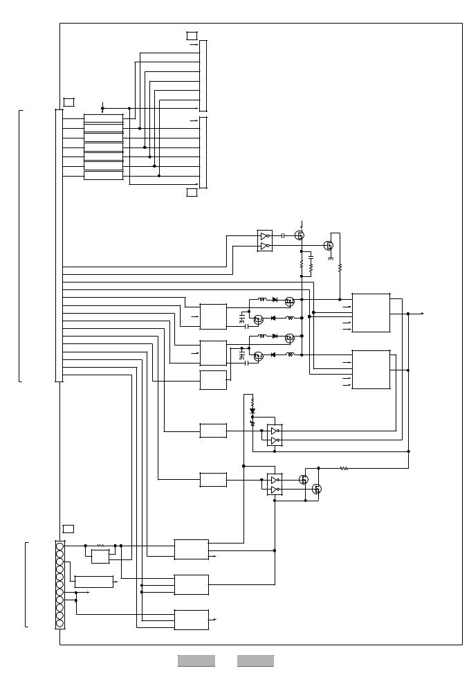
1 |
2 |
3 |
4 |
3.1.2 43 Y DRIVE ASSY
A
• Block Diagram
|
|
|
|
43 Y DRIVE ASSY |
Y2 |
|
|
|
|
|
|
|
|
||
|
|
|
|
|
|
|
VH |
|
|
|
|
|
|
|
|
|
|
|
|
|
|
|
|
CN2101 |
|
43 SCAN B ASSY |
|
|
|
||
|
|
|
|
|
|
|
|
|
|
|
To |
|
|
|
|
|
|
|
|
IC5V |
|
|
|
|
|
|
|
|
|
|
|
|
|
|
|
Y1 |
|
|
|
|
|
|
|
|
|
|
|
|
|
CLK1 |
|
Photo Coupler |
|
|
VH |
|
|
|
|
|
|
|
|
|
|
|
|
|
|
|
|
|
|
|
|
|
|
|
|
B |
|
CE |
|
Photo Coupler |
|
|
|
|
|
|
|
|
|
|
|
|
CLK2 |
|
Photo Coupler |
|
|
|
|
|
|
|
|
|
|
|
|
|
|
|
|
|
|
CN2102 |
|
|
|
|
|
|
|||
|
|
CLR |
|
Photo Coupler |
|
|
|
|
To |
|
|
|
|
||
|
|
OC2 |
|
Photo Coupler |
|
|
|
|
|
|
43 SCAN A ASSY |
|
|
|
|
|
|
|
|
|
|
|
|
|
|
|
|
|
|
||
|
|
OC1 |
|
Photo Coupler |
|
|
|
|
|
|
|
|
|
|
|
|
|
SI |
|
Photo Coupler |
|
|
|
|
|
|
|
|
|
|
|
|
ASSYVIDEO |
|
|
|
|
|
Y3 |
|
|
|
|
|
|
|
|
|
|
CN2001 |
|
|
|
|
|
|
|
|
VSUS |
|
|
|
|
|
|
|
|
|
|
|
|
|
|
|
|
|
|
|
|
|
|
|
|
|
|
|
|
|
|
|
|
IC2203 |
|
|
|
|
|
|
|
|
|
|
|
|
|
|
|
YPR-U |
|
|
|
|
|
|
|
|
|
|
|
|
|
|
|
YSOFT-D |
|
|
|
C |
DIGITAL |
|
|
|
|
|
|
|
|
|
|
|
|
|
|
|
YSUS-G |
|
|
|
|
|
|
|
|
|
|
|
|
|
|
|
|
YPR-U |
|
|
|
|
|
|
|
|
|
|
|
|
|
|
|
YSOFT-D |
|
|
|
|
|
|
|
|
|
YSUS-G |
|
|
|
|
|
|
|
|
|
|
|
|
|
|
|
|
|
|
|
|
From |
YSUS-B |
|
|
|
|
|
|
|
|
|
YSUS-B |
|
|
|
|
|
|
|
|
|
|
|
|
|
|
|
|
|
||
|
YSUS-U2 |
|
|
|
|
YSUS |
IC2201 |
|
|
Mask Module |
|
||||
|
|
YSUS-D2 |
|
|
|
|
-U2 |
|
|
|
|
L2202 |
VSUS |
IC2303 |
To |
|
|
YSUS-U1 |
|
|
|
|
|
|
|
|
HB |
|
|
||
|
|
|
|
|
|
5V |
|
|
|
|
|
SCAN ASSY |
|||
|
|
YSUS-D1 |
|
|
|
|
DRIVER |
|
5V |
STK795-511 |
|||||
|
|
|
|
|
|
|
L2203 |
|
|||||||
|
|
|
|
|
|
|
|
|
|
|
|
|
|||
|
|
YSUS-MSK |
|
|
|
|
|
|
|
|
|
|
|
||
|
|
|
|
|
|
YSUS-D2 |
|
|
|
|
SUS |
16.5V |
|
|
|
|
|
YOFS |
|
|
|
|
YSUS-U1 |
|
IC2202 |
GND |
|
|
|
||
|
|
YSUS-PD |
|
|
|
|
|
|
|
|
L2204 |
|
|
|
|
|
|
|
|
|
|
|
|
|
|
HB |
|
|
|
|
|
|
SCN_5V_PD |
|
|
|
|
5V |
|
|
|
|
|
|
|
||
|
|
|
|
|
DRIVER |
|
|
Mask Module |
|
||||||
|
|
Y_DD_PD |
|
|
|
|
|
L2205 |
|
|
|||||
|
|
|
|
|
|
|
|
|
|
|
VSUS |
|
|||
|
|
SCAN_PD |
|
|
|
|
YSUS-D1 |
|
|
|
|
SUS |
|
|
|
D |
|
|
|
|
|
|
|
|
|
|
IC2307 |
|
|||
|
|
|
|
|
|
|
|
|
XSUS |
GND |
|
|
|||
|
YDRIVE_PD |
|
|
|
|
|
|
|
5V |
STK795-511 |
|
||||
|
|
|
|
|
|
|
|
|
|
|
P.D. |
|
|
|
|
|
|
|
|
|
|
|
|
|
|
Circuit |
|
16.5V |
|
|
|
|
|
|
|
|
|
|
|
|
|
IC2302 |
IC2304 |
|
|
|
|
|
|
|
|
|
|
YSUS-MSK |
|
|
Photo |
|
|
|
|
||
|
|
|
|
|
|
|
|
|
Coupler |
|
|
|
|
||
|
|
|
|
|
|
|
YOFS |
|
|
IC2308 |
IC2309 |
|
|
|
|
|
|
|
|
|
|
|
|
|
Photo |
|
|
|
|
||
|
|
|
|
|
|
|
|
|
Coupler |
|
|
|
|
||
E |
|
|
|
|
|
|
|
|
|
|
|
|
|
|
|
|
UNIT |
16.5V |
1 |
Y4 |
|
|
IC5V, VF |
|
|
VF- |
|
|
|
|
|
|
|
|
|
|
|
|
|
|
|
||||||
|
|
|
CN2301 |
|
|
|
|
|
|
VF+ |
|
|
|
|
|
|
|
|
|
|
|
|
|
|
|
|
|
|
|
|
|
|
SUPPLY |
DGND |
2 |
P.D. |
|
|
D-D CONV. |
IC5V |
|
|
|
||||
|
N.C. |
5 |
DET. |
|
IC5V UVP |
|
|
|
|
|
|
|
|||
|
|
6.5V |
3 |
|
|
|
|
|
|
|
|
|
|
|
|
|
|
DGND |
4 |
IC2305 |
|
|
|
|
|
|
|
|
|
|
|
|
|
|
|
|
|
|
|
|
|
|
|
|
|
|
|
|
POWER |
N.C. |
9 |
REGULATOR |
5V |
VOFS OVP |
VOFS |
|
|
|
VOFS |
|
|
|
|
|
|
N.C. |
6 |
|
|
VOFS UVP |
D-D CONV. |
|
|
|
|
|
|||
|
|
VSUS |
7 |
VSUS |
|
|
|
|
|
|
|||||
|
|
|
|
|
|
|
|
|
|
|
|
|
|||
|
|
VSUS |
8 |
|
|
|
|
|
|
|
|
|
|
|
|
F |
From |
SUSGND |
10 |
|
|
VSUS |
VH D-D |
|
|
|
|
|
|
|
|
|
|
|
VH OVP |
|
|
|
VH |
|
|
|
|
||||
|
|
SUSGND |
11 |
|
|
|
|
|
|
|
|
|
|||
|
|
|
|
VH UVP |
CONV. |
|
|
|
|
|
|
|
|
||
|
|
|
|
|
|
|
|
|
|
|
|
|
|
|
|
|
24 |
|
|
|
|
|
|
|
PDP-434PU |
|
|
|
|||
|
|
1 |
|
|
|
2 |
|
|
|
|
|
3 |
|
|
4 |

5 |
6 |
7 |
8 |
3.1.3 43 X DRIVE ASSY
• Block Diagram
A
|
|
|
43 X DRIVE ASSY |
|
|
|
|
|
|
||
|
|
|
X1 |
|
|
|
|
|
|
|
|
ASSY |
XSUS-G |
|
|
|
|
|
|
|
XSUS-G |
|
|
|
|
|
|
|
|
|
XSUS-B |
|
|
||
|
|
|
|
|
|
|
|
|
|
||
|
XSUS-B |
|
|
|
|
|
|
|
|
|
|
|
|
|
|
|
|
|
|
|
|
|
|
VIDEODIGITAL |
XSUS-U2 |
|
|
|
XSUS IC1101 |
|
L1102 |
|
Mask Module |
||
XSUS-D2 |
CN1001 |
|
|
-U2 |
|
|
|
VSUS |
PSUS |
||
|
|
|
|
HB |
|
|
|||||
XSUS-U1 |
|
|
|
|
|
|
|
IC1203 |
|||
|
|
|
|
5V |
|
HB |
|
|
|
||
|
XSUS-D1 |
|
|
|
DRIVER |
|
L1103 |
5V |
STK795-510 |
||
|
|
|
|
|
|
|
|
|
|||
|
XSUS-MSK |
|
|
|
|
|
|
|
|
||
|
|
|
|
XSUS-D2 |
|
|
SUS |
|
16.5V |
|
|
|
XCP-MSK |
|
|
|
XSUS-U1 |
IC1102 |
GND |
|
|
||
|
XNR-D |
|
|
|
|
|
|
L1104 |
|
|
|
|
|
|
|
|
|
|
|
|
|
|
|
From |
XSUS_PD |
|
|
|
5V |
DRIVER |
|
|
|
|
|
XDRV_PD |
|
|
|
XSUS-D1 |
SUS |
|
IC1207 |
||||
|
XDD_PD |
|
|
|
|
|
|
|
L1105 |
VSUS |
Mask Module |
|
|
|
|
|
|
|
|
|
|
|
|
|
|
|
|
|
|
XSUS |
GND |
|
STK795-510 |
||
|
|
|
|
|
|
|
|
5V |
|||
|
|
|
|
|
|
|
P.D. |
|
|
|
|
|
|
|
|
|
|
Circuit |
|
|
16.5V |
|
|
|
|
|
|
|
XCP-MSK |
Charge Pump |
VCP |
|
|
||
|
|
|
|
|
|
|
|
||||
|
|
|
|
|
|
|
Circuit |
|
|
|
|
|
|
|
|
|
|
IC1202 |
|
|
|
|
|
|
|
|
|
|
XSUS-MSK |
Photo |
|
|
|
|
|
|
|
|
|
|
|
Coupler |
|
|
|
|
|
|
|
|
|
|
|
|
|
|
XNR P.D. |
|
|
|
|
|
|
|
|
|
|
|
DET. |
|
|
|
|
|
X2 |
|
|
|
|
|
|
|
|
UNIT |
|
CN1201 |
|
|
|
|
|
|
|
|
|
DGND |
2 |
P.D. |
XNR-D |
|
|
|
|
|
|
||
|
16.5V |
1 |
|
|
IC1204 |
|
|
|
|
||
|
|
|
|
|
|
|
|
|
|||
SUPPLY |
N.C. |
6 |
DET. |
|
|
|
|
|
|
|
|
|
6.5V |
3 |
|
|
|
|
|
|
|
|
|
|
DGND |
4 |
IC1205 |
|
|
|
|
|
|
|
|
|
N.C. |
5 |
REGULATOR |
5V |
|
|
|
|
|
|
|
POWER |
|
|
|
|
|
|
|
|
|
||
SUSGND |
10 |
VSUS |
P.D. |
|
|
|
|
|
|
|
|
|
VSUS |
7 |
|
|
|
|
|
|
|
|
|
|
VSUS |
8 |
|
|
VSUS |
|
|
|
|
|
|
|
N.C. |
9 |
|
VRN OVP |
|
|
|
|
|
|
|
|
|
|
|
|
|
|
|
|
|||
|
|
|
|
|
|
|
|
|
|
|
|
From |
SUSGND |
11 |
|
|
D-D CONV. |
VRN-225V |
|
|
|
||
|
|
T1401 |
|
|
|
|
|
|
|||
|
|
|
|
|
|
|
|
|
|||
|
|
|
|
|
|
|
|
|
|
|
|
|
N.C. |
12 |
|
VRN UVP P.D. |
|
|
|
|
|
|
|
X CONNECTOR ASSY
To
B
C
D
E
F
|
|
|
|
|
|
|
|
|
PDP |
-434PU |
7 |
25 |
|
5 |
6 |
|
|
|
8 |
|
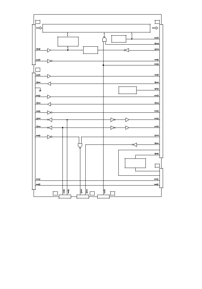
1 |
2 |
3 |
4 |
3.1.4 PANEL IF ASSY
A |
• Block Diagram |
|
|
|
|
|
|
|
|
|
|
|
||
|
|
|
|
PANEL IF ASSY |
|
|
|
|
|
|
|
|
||
|
|
|
R3 |
|
|
|
|
|
|
|
|
|
R4 |
|
|
|
TMDS |
|
IC4202 |
|
|
|
|
|
|
|
|
|
|
|
|
|
TMDS RECEIVER |
|
|
|
|
|
|
|
|
|||
|
CONNECTOR |
|
CN4003 |
|
|
|
|
|
|
|
|
|||
|
|
|
|
Q4215 |
|
|
Q4017 |
IC4205 |
|
|
RSTBTMD |
|||
|
|
|
|
|
|
|
|
RESET IC |
|
|
||||
|
|
|
|
|
5V ↔ 3.3V |
|
|
NOR |
|
|
|
|||
|
|
|
|
IC4206 |
|
|
|
|
|
|
|
|||
|
|
|
|
I2C LEVEL SHIFT |
|
|
|
|
|
|
|
DVI_MUTE |
||
|
|
6: DDC_SCL |
|
I2C BUFFER |
|
|
|
IC4201 |
|
|
Q4203 INV |
|
|
|
|
|
|
|
|
|
|
|
|
|
|
|
*DDC_WP |
||
|
|
7: DDC_SDA |
|
|
|
|
|
DDC_ROM |
|
|
|
|
||
|
|
|
|
|
|
|
|
|
|
|
|
|||
B |
DVI |
|
|
Q4004 |
|
|
|
|
|
|
|
|
|
|
|
|
INV |
|
|
|
|
|
|
|
|
|
|
||
|
|
|
|
|
|
|
|
|
|
|
|
|
||
|
|
14: DDC_+5V |
|
|
|
|
|
|
|
|
|
|
|
DVI_OFF |
|
|
|
|
|
|
|
|
|
|
|
|
|
|
OP_DET |
|
|
|
R2 |
|
|
|
|
|
|
|
|
|
|
|
|
|
|
|
IC4006 BUF |
|
|
|
|
|
|
|
|
|
|
|
|
11: MTXD |
|
|
|
|
|
|
|
|
|
|
|
RXD0 |
|
|
|
|
IC4006 BUF |
|
|
|
|
|
|
|
|
|
|
|
|
2: MRXD |
|
|
|
|
|
|
|
|
|
|
CN4004 |
TXD0 |
|
|
3: P_ST_B |
|
|
|
|
|
|
|
|
IC4002 |
|
B_SCL, B_SDA |
|
|
|
|
|
|
|
|
|
|
|
|
|
|||
|
|
|
|
|
|
|
|
|
|
|
BACKUP ROM |
|
|
|
|
|
|
|
IC4006 BUF |
|
|
|
|
|
|
|
|
|
|
|
|
|
|
|
|
|
|
|
|
|
|
|
|
|
|
|
10: MR_ST_B |
|
|
|
|
|
|
|
|
|
|
|
MR_ST_B |
|
|
|
|
IC4006 BUF |
|
|
|
|
|
|
|
|
|
|
|
CONNECTORMDR |
7: REQ |
CN4002 |
|
|
|
|
|
|
|
|
|
|
REQ_MD |
C |
|
Q4004 INV |
|
|
|
|
|
|
|
|
|
|
||
|
|
|
|
|
|
|
|
|
|
|
|
|
||
|
|
8: STB3V |
|
|
|
|
|
|
|
|
|
|
|
MR_AC_OFF |
|
|
|
|
Q4006 INV |
|
|
|
|
|
Q4006 INV |
IC4006 BUF |
|
|
|
|
|
9: KEY_B |
|
|
|
|
|
|
|
|
|
|
|
KEY_B |
|
|
|
|
Q4006 INV |
|
|
|
|
|
Q4006 INV |
IC4006 BUF |
|
|
|
|
|
14: REM_B |
|
|
|
|
|
|
|
|
|
|
|
REM_B |
|
|
|
|
Q4009 INV |
|
|
|
|
|
|
|
|
|
|
|
|
15: STB_MT |
|
|
|
|
|
|
|
|
|
|
|
LED_R_B |
|
|
|
|
|
|
|
|
|
|
|
Q4011 INV |
|
|
|
|
|
|
|
|
|
Q4007, |
|
|
|
|
|
|
|
LED_G_B |
|
|
|
|
|
|
Q4011 |
|
|
|
|
|
|
|
A_NG,A_MUTE,STB_SW, |
|
|
|
|
|
|
NOR |
|
|
|
|
|
|
|
|
|
|
|
|
|
|
|
|
|
|
|
|
|
FOCUS,TRUBASS,SRS |
|
|
|
|
|
|
|
|
|
|
|
|
|
|
|
|
|
|
|
|
|
|
|
|
|
|
|
|
|
|
A_SCL, A_SDA |
D |
|
|
|
|
|
|
|
|
|
|
Q4001 |
|
|
|
|
|
|
|
|
|
|
|
|
|
|
5V ↔ |
3.3V |
R7 |
|
|
|
|
|
|
|
|
|
|
|
|
I2C LEVEL SHIFT |
|
||
|
|
13: AUDIO_R |
|
|
|
|
|
|
|
|
|
|
CN4009 |
R_IN |
|
|
20: AUDIO_L |
|
|
|
|
|
|
|
|
|
|
|
L_IN |
|
|
|
|
R8 |
|
|
|
R6 |
|
R5 |
|
|
|
|
|
|
|
|
|
CN4010 |
CN4007 |
CN4006 |
|
|
|
|
|||
|
|
|
|
|
REM |
KEY |
LED R |
LED G |
|
OP DET |
|
|
|
|
E
F
|
|
|
|
|
|
|
26 |
|
PDP-434PU |
|
|
||
1 |
2 |
|
|
|
3 |
4 |

|
5 |
|
6 |
|
|
|
|
7 |
8 |
|
• Voltages |
|
|
|
|
|
|
|
|
|
|
CN4001 (R1) < |
POWER SUPPLY UNIT > |
|
|
|
||||||
No. |
Signal Name |
I/O |
Signal Description |
|
Voltages at NTSC Signal Input |
|
||||
1 |
6.5V |
I |
+6.5V power supply |
|
+6.8VDC |
|
||||
2 |
6.5V |
I |
+6.5V power supply |
|
+6.8VDC |
|
||||
3 |
Vcc_GND |
− |
GND |
|
|
|
||||
4 |
Vcc_GND |
− |
GND |
|
|
|
||||
5 |
STB3.3V |
I |
Power supply +3.3V input of module UCOM at panel side |
|
+3.3VDC |
|
||||
6 |
STB_GND |
− |
GND |
|
|
|
||||
7 |
STB3.3MUTE |
O |
Standby control (+3.3V mute) |
|
+6.7VDC |
|
||||
8 |
AC_DET |
I |
Primary power supply (AC) state input at panel side |
|
+3.0VDC |
|
||||
CN4002 (R2) < |
MEDIA RECEIVER > |
|
|
|
||||||
No. |
Signal Name |
I/O |
Signal Description |
|
Voltages at NTSC Signal Input |
|
||||
1 |
MR_ST_B |
I |
Connection state detecting signal with MDR |
|
0VDC |
|
||||
2 |
MRXD |
O |
UART communication transmission data with the main UCOM (external PC) |
0-3.3V amplitude square wave |
|
|||||
|
|
|
at MDR side |
|
|
|
||||
3 |
P_ST_B |
O |
Connection state output for the MDR |
|
0VDC |
|
||||
4 |
ACT3V |
O |
Power supply +3.3V output of module UCOM at panel side |
|
+3.3VDC |
|
||||
5 |
AC_OFF |
O |
Primary power supply (AC) state output at panel side |
|
0VDC |
|
||||
6 |
GND |
− |
GND |
|
|
|
||||
7 |
REQ |
O |
Communication request to the main UCOM (external PC) at the MDR |
0-3.3V amplitude square wave |
|
|||||
8 |
STB3V |
I |
Standby power supply (+3.3V) input from the MDR |
|
+3.3VDC |
|
||||
9 |
KEY_B |
O |
Function key code signal output at panel side |
|
0-3.3V amplitude square wave (at key |
|
||||
|
operation) |
|
||||||||
|
|
|
|
|
|
|
|
|
|
|
10 |
MR_ST_B' |
I |
Connection state detecting signal with the MDR |
|
0VDC |
|
||||
11 |
MTXD |
I |
UART communication receive data with the main UCOM (external PC) at |
0-3.3V amplitude square wave |
|
|||||
the MDR side |
|
|
||||||||
|
|
|
|
|
|
|||||
12 |
GND |
− |
GND |
|
|
|
||||
13 |
AUDIO_R |
I |
R ch audio signal input |
|
Audio R signal |
|
||||
14 |
REM_B |
O |
Remote control code signal output |
|
0-3.3V amplitude square wave (at remocon |
|
||||
|
code transmission) |
|
||||||||
|
|
|
|
|
|
|
|
|
|
|
15 |
STB_MT |
I |
Standby control input |
|
0VDC |
|
||||
16 |
GND |
− |
GND |
|
|
|
||||
17 |
NC |
− |
Not connected |
|
− |
|
||||
18 |
FIELD |
I |
FIELD control signal |
|
0VDC |
|
||||
19 |
GND |
− |
GND |
|
|
|
||||
20 |
AUDIO_L |
I |
L ch audio signal input |
|
Audio L signal |
|
||||
CN4003 (R3) < |
MEDIA RECEIVER > |
|
|
|
||||||
|
|
|
|
|
||||||
No. |
Signal Name |
I/O |
Signal Description |
|
Voltages at NTSC Signal Input |
|
||||
1 |
RX2- |
I |
DVI signal |
|
DVI differential signal (-) |
|
||||
2 |
RX2+ |
I |
DVI signal |
|
DVI differential signal (+) |
|
||||
3 |
GND |
− |
GND |
|
|
|
||||
4 |
N.C |
− |
Not connected |
|
− |
|
||||
5 |
N.C |
− |
Not connected |
|
− |
|
||||
6 |
DDC_SCL |
I |
I2C signal for DDC |
|
|
|
||||
|
0-5V amplitude square wave |
|
||||||||
7 |
DDC_SDA |
I |
I2C signal for DDC |
|
0-5V amplitude square wave |
|
||||
8 |
N.C |
− |
Not connected |
|
− |
|
||||
9 |
RX1- |
I |
DVI signal |
|
DVI differential signal (-) |
|
||||
10 |
RX1+ |
I |
DVI signal |
|
DVI differential signal (+) |
|
||||
11 |
GND |
− |
GND |
|
|
|
||||
12 |
N.C |
− |
Not connected |
|
− |
|
||||
13 |
N.C |
− |
Not connected |
|
− |
|
||||
14 |
DDC_+5V |
I |
I2C power supply for DDC |
|
+5VDC |
|
||||
15 |
GND |
− |
GND |
|
|
|
||||
16 |
HPD |
O |
Hot plug detection |
|
+5VDC |
|
||||
17 |
RX0- |
I |
DVI signal |
|
DVI differential signal (-) |
|
||||
18 |
RX0+ |
I |
DVI signal |
|
DVI differential signal (+) |
|
||||
19 |
GND |
− |
GND |
|
|
|
||||
20 |
N.C |
− |
Not connected |
|
− |
|
||||
21 |
N.C |
− |
Not connected |
|
− |
|
||||
|
|
|
|
|
|
|
|
|
|
|
|
|
|
|
PDP |
-434PU |
|
7 |
27 |
||
|
5 |
|
6 |
|
|
|
|
8 |
|
|
A
B
C
D
E
F

|
|
|
1 |
|
2 |
|
|
|
3 |
4 |
|
|
• Voltages |
|
|
|
|
|
|
|
|||
A |
|
CN4003 (R3) < |
MEDIA RECEIVER > |
|
|
||||||
|
|
|
|
|
|
|
|
|
|||
|
|
No. |
|
Signal Name |
I/O |
Signal Description |
|
Voltages at NTSC Signal Input |
|||
|
|
22 |
GND |
− |
GND |
|
|
||||
|
|
23 |
RXC+ |
I |
DVI signal |
|
DVI differential signal (-) |
||||
|
|
24 |
RXC- |
I |
DVI signal |
|
DVI differential signal (+) |
||||
|
|
CN4006 (R5) < |
TRAP SW > |
|
|
||||||
|
|
|
|
|
|
|
|
|
|||
|
|
No. |
|
Signal Name |
I/O |
Signal Description |
|
Voltages at NTSC Signal Input |
|||
|
|
1 |
OP_DET |
I |
Rear panel open detecting signal |
|
0VDC |
||||
|
|
2 |
N.C |
− |
Not connected |
|
− |
||||
B |
|
3 |
GND |
− |
GND |
|
|
||||
|
CN4007 (R6) < |
PANEL LED ASSY > |
|
|
|||||||
|
|
|
|
||||||||
|
|
|
|
|
|
|
|
|
|
||
|
|
No. |
Signal Name |
I/O |
|
Signal Description |
|
Voltages at NTSC Signal Input |
|||
|
|
1 |
|
LED_G |
O |
LED control (green) |
|
+2.1VDC |
|||
|
|
2 |
|
LED_R |
O |
LED control (red) |
|
0VDC |
|||
|
|
3 |
|
AC_OFF |
O |
Primary power supply (AC) state output at the panel side |
0VDC |
||||
|
|
CN4009 (R7) < |
HD AUDIO AMP ASSY > |
|
|
||||||
|
|
|
|
|
|
|
|
||||
|
|
No. |
Signal Name |
I/O |
Signal Description |
|
Voltages at NTSC Signal Input |
||||
|
|
1 |
|
A_NG |
I |
Abnormal detecting signal of the audio block |
|
+3.3V DC |
|||
C |
|
2 |
|
V+6.5 |
O |
+6.5V power supply |
|
+6.8V DC |
|||
|
3 |
|
GNDA |
− |
GND |
|
|
||||
|
|
|
|
|
|||||||
|
|
4 |
|
L_IN |
O |
L ch audio signal |
|
Audio L signal |
|||
|
|
5 |
|
GNDA |
− |
GND |
|
|
|||
|
|
6 |
|
R_IN |
O |
R ch audio signal |
|
Audio R signal |
|||
|
|
7 |
|
ST_BY |
O |
Standby signal of the audio block |
|
+3.3V DC |
|||
|
|
8 |
|
A_MUTE |
O |
Audio mute signal input |
|
0V DC |
|||
|
|
9 |
|
SCL |
O |
I2C control signal for audio |
|
0-3.3V amplitude square wave |
|||
|
|
10 |
|
SDA |
O |
I2C control signal for audio |
|
0-3.3V amplitude square wave |
|||
|
|
11 |
|
FOCUS |
O |
Focus function control signal |
|
+3.3V DC |
|||
|
|
12 |
|
SRS |
O |
SRS function control signal |
|
+3.3V DC |
|||
|
|
13 |
|
TRUBASS |
O |
TRUBASS function control signal |
|
+3.3V DC |
|||
D |
|
|
|
|
|
|
|
|
|
|
|
|
CN4010 (R8) < |
PANEL IR ASSY, KEY CONTROL ASSY > |
|
|
|||||||
|
|
|
|
||||||||
|
|
|
|
|
|
|
|||||
|
|
No. |
Signal Name |
I/O |
Signal Description |
|
Voltages at NTSC Signal Input |
||||
|
|
1 |
|
STB3V |
O |
+3.3V power supply |
|
+3.3V DC |
|||
|
|
2 |
|
STBGND |
− |
GND |
|
|
|||
|
|
3 |
|
REM |
I |
Remote control code signal input |
|
0-3.3V amplitude square wave (at remocon |
|||
|
|
|
|
code transmission) |
|||||||
|
|
|
|
|
|
|
|
|
|
|
|
|
|
4 |
|
STB+3V |
O |
+3.3V power supply |
|
+3.3V DC |
|||
|
|
5 |
|
KEY |
I |
Function key code signal input at the panel side |
|
0-3.3V amplitude square wave (at key operation) |
|||
|
|
6 |
|
STBGND |
− |
GND |
|
|
|||
E |
|
CN4801 (SW1) < |
KEY CONTROL ASSY > |
|
|
||||||
|
|
|
|
|
|
|
|||||
|
|
No. |
Signal Name |
I/O |
Signal Description |
|
Voltages at NTSC Signal Input |
||||
|
|
1 |
|
STBGND |
− |
GND |
|
0V DC |
|||
|
|
2 |
|
G1 |
O |
Key scan signal |
|
0V DC |
|||
|
|
3 |
|
G0 |
O |
Key scan signal |
|
0V DC |
|||
|
|
4 |
|
D5 |
I |
Key scan signal |
|
+3.3V DC |
|||
|
|
5 |
|
D6 |
I |
Key scan signal |
|
+3.3V DC |
|||
|
|
6 |
|
D7 |
I |
Key scan signal |
|
+3.3V DC |
|||
F |
|
|
|
|
|
|
|
|
|
|
|
|
28 |
|
|
|
|
|
|
|
|
|
|
|
|
|
|
|
|
PDP-434PU |
|
|
|||
|
|
|
1 |
|
2 |
|
|
|
3 |
4 |
|

5 |
6 |
7 |
8 |
• Voltages
CN4004 (R4) < |
DIGITAL VIDEO ASSY > (1/2) |
|
|
|
||||||
|
|
|
|
|
|
|
|
|||
|
No. |
Signal Name |
I/O |
Signal Description |
|
Voltages at NTSC Signal Input |
|
|||
|
1 |
GND |
− |
GND |
|
|
|
|||
|
2 |
GND |
− |
GND |
|
|
|
|||
|
3 |
|
|
Not connected |
|
− |
|
|||
|
4 |
|
|
Not connected |
|
− |
|
|||
|
5 |
BA0 |
O |
8bit video signal output (BLUE even number) |
|
0-3.3V amplitude square wave |
|
|||
|
6 |
BA1 |
O |
8bit video signal output (BLUE even number) |
|
0-3.3V amplitude square wave |
|
|||
|
7 |
BA2 |
O |
8bit video signal output (BLUE even number) |
|
0-3.3V amplitude square wave |
|
|||
|
8 |
BA3 |
O |
8bit video signal output (BLUE even number) |
|
0-3.3V amplitude square wave |
|
|||
|
9 |
BA4 |
O |
8bit video signal output (BLUE even number) |
|
0-3.3V amplitude square wave |
|
|||
|
10 |
BA5 |
O |
8bit video signal output (BLUE even number) |
|
0-3.3V amplitude square wave |
|
|||
|
11 |
BA6 |
O |
8bit video signal output (BLUE even number) |
|
0-3.3V amplitude square wave |
|
|||
|
12 |
BA7 |
O |
8bit video signal output (BLUE even number) |
|
0-3.3V amplitude square wave |
|
|||
|
13 |
GND |
− |
GND |
|
|
|
|||
|
14 |
GND |
− |
GND |
|
|
|
|||
|
15 |
|
|
Not connected |
|
− |
|
|||
|
16 |
|
|
Not connected |
|
− |
|
|||
|
17 |
GA0 |
O |
8bit video signal output (GREEN even number) |
|
0-3.3V amplitude square wave |
|
|||
|
18 |
GA1 |
O |
8bit video signal output (GREEN even number) |
|
0-3.3V amplitude square wave |
|
|||
|
19 |
GA2 |
O |
8bit video signal output (GREEN even number) |
|
0-3.3V amplitude square wave |
|
|||
|
20 |
GA3 |
O |
8bit video signal output (GREEN even number) |
|
0-3.3V amplitude square wave |
|
|||
|
21 |
GA4 |
O |
8bit video signal output (GREEN even number) |
|
0-3.3V amplitude square wave |
|
|||
|
22 |
GA5 |
O |
8bit video signal output (GREEN even number) |
|
0-3.3V amplitude square wave |
|
|||
|
23 |
GA6 |
O |
8bit video signal output (GREEN even number) |
|
0-3.3V amplitude square wave |
|
|||
|
24 |
GA7 |
O |
8bit video signal output (GREEN even number) |
|
0-3.3V amplitude square wave |
|
|||
|
25 |
GND |
− |
GND |
|
|
|
|||
|
26 |
GND |
− |
GND |
|
|
|
|||
|
27 |
|
|
Not connected |
|
− |
|
|||
|
28 |
|
|
Not connected |
|
− |
|
|||
|
29 |
RA0 |
O |
8bit video signal output (RED even number) |
|
0-3.3V amplitude square wave |
|
|||
|
30 |
RA1 |
O |
8bit video signal output (RED even number) |
|
0-3.3V amplitude square wave |
|
|||
|
31 |
RA2 |
O |
8bit video signal output (RED even number) |
|
0-3.3V amplitude square wave |
|
|||
|
32 |
RA3 |
O |
8bit video signal output (RED even number) |
|
0-3.3V amplitude square wave |
|
|||
|
33 |
RA4 |
O |
8bit video signal output (RED even number) |
|
0-3.3V amplitude square wave |
|
|||
|
34 |
RA5 |
O |
8bit video signal output (RED even number) |
|
0-3.3V amplitude square wave |
|
|||
|
35 |
RA6 |
O |
8bit video signal output (RED even number) |
|
0-3.3V amplitude square wave |
|
|||
|
36 |
RA7 |
O |
8bit video signal output (RED even number) |
|
0-3.3V amplitude square wave |
|
|||
|
37 |
GND\ |
− |
GND |
|
|
|
|||
|
38 |
DCLK |
O |
Synchronous signal output (clock) |
|
0-3.3V amplitude square wave (42.5MHz) |
|
|||
|
39 |
GND |
− |
GND |
|
|
|
|||
|
40 |
DEI |
O |
Synchronous signal output (data enable) |
|
0-3.3V amplitude square wave (positive polarity) |
|
|||
|
41 |
HDI |
O |
Synchronous signal output (Horizontal sync.) |
|
0-3.3V amplitude square wave (negative polarity) |
|
|||
|
42 |
VDI |
O |
Synchronous signal output (Vertical sync.) |
|
0-3.3V amplitude square wave (negative polarity) |
|
|||
|
43 |
FIELD |
O |
FIELD control signal |
|
0V DC |
|
|||
|
44 |
APL_DT |
|
Not connected |
|
− |
|
|||
|
45 |
|
|
Not connected |
|
− |
|
|||
|
46 |
|
|
Not connected |
|
− |
|
|||
|
47 |
BB0 |
O |
8bit video signal output (BLUE odd number) |
|
0-3.3V amplitude square wave |
|
|||
|
48 |
BB1 |
O |
8bit video signal output (BLUE odd number) |
|
0-3.3V amplitude square wave |
|
|||
|
49 |
BB2 |
O |
8bit video signal output (BLUE odd number) |
|
0-3.3V amplitude square wave |
|
|||
|
50 |
BB3 |
O |
8bit video signal output (BLUE odd number) |
|
0-3.3V amplitude square wave |
|
|||
|
51 |
BB4 |
O |
8bit video signal output (BLUE odd number) |
|
0-3.3V amplitude square wave |
|
|||
|
52 |
BB5 |
O |
8bit video signal output (BLUE odd number) |
|
0-3.3V amplitude square wave |
|
|||
|
53 |
BB6 |
O |
8bit video signal output (BLUE odd number) |
|
0-3.3V amplitude square wave |
|
|||
|
54 |
BB7 |
O |
8bit video signal output (BLUE odd number) |
|
0-3.3V amplitude square wave |
|
|||
|
55 |
GND |
− |
GND |
|
|
|
|||
|
56 |
GND |
− |
GND |
|
|
|
|||
|
57 |
|
|
Not connected |
|
− |
|
|||
|
58 |
|
|
Not connected |
|
− |
|
|||
|
|
|
|
|
|
|
|
|
|
|
|
|
|
|
|
PDP |
-434PU |
7 |
29 |
||
|
|
5 |
|
6 |
|
|
|
8 |
|
|
A
B
C
D
E
F
 Loading...