


ORDER NO.
ARP3354
PDP-5071PU
PLASMA DISPLAY SYSTEM
PDP-5071PU
PDP-5070PU
THIS MANUAL IS APPLICABLE TO THE FOLLOWING MODEL(S) AND TYPE(S).
Model |
Type |
Power Requirement |
Remarks |
|
|
|
|
PDP-5071PU |
KUCXC |
AC 120 V |
|
|
|
|
|
PDP-5070PU |
KUCXC |
AC 120 V |
|
|
|
|
|
This service manual should be used together with the following manual(s).
Model No. |
Order No. |
Remarks |
|
|
|
PDP-5071PU, PDP-5070PU |
ARP3355 |
SCHEMATIC DIAGRAM, PCB CONNECTION DIAGRAM |
|
|
|
For details, refer to "Important Check Points for good servicing".
PIONEER CORPORATION 4-1, Meguro 1-chome, Meguro-ku, Tokyo 153-8654, Japan
PIONEER ELECTRONICS (USA) INC. P.O. Box 1760, Long Beach, CA 90801-1760, U.S.A.
PIONEER EUROPE NV Haven 1087, Keetberglaan 1, 9120 Melsele, Belgium
PIONEER ELECTRONICS ASIACENTRE PTE. LTD. 253 Alexandra Road, #04-01, Singapore 159936
 PIONEER CORPORATION 2006
T-IZV AUG. 2006 printed in Japan

1 |
2 |
3 |
4 |
1. NOTES ON SERVICE VISIT
1.1 SAFETY INFORMATION
A
This service manual is intended for qualified service technicians ; it is not meant for the casual do-it-yourselfer. Qualified technicians have the necessary test equipment and tools, and have been trained to properly and safely repair complex products such as those covered by this manual.
Improperly performed repairs can adversely affect the safety and reliability of the product and may void the warranty. If you are not qualified to perform the repair of this product properly and safely, you should not risk trying to do so and refer the repair to a qualified service technician.
WARNING
B
This product contains lead in solder and certain electrical parts contain chemicals which are known to the state of California to cause cancer, birth defects or other reproductive harm.
Health & Safety Code Section 25249.6 - Proposition 65
NOTICE
(FOR CANADIAN MODEL ONLY)
Fuse symbols 

 (fast operating fuse) and/or

 (slow operating fuse) on PCB indicate that replacement parts must be of identical designation.
REMARQUE
(POUR MODÈLE CANADIEN SEULEMENT)
Les symboles de fusible 
 (fusible de type rapide) et/ou
 (fusible de type lent) sur CCI indiquent que les pièces
de remplacement doivent avoir la même désignation.
C
SAFETY PRECAUTIONS
NOTICE : Comply with all cautions and safety related notes located on or inside the cabinet and on the chassis.
The following precautions should be observed :
1. When service is required, even though the PDP UNIT an isolation transformer should be inserted between the power line
Dand the set in safety before any service is performed.
2.When replacing a chassis in the set, all the protective devices must be put back in place, such as barriers, nonmetallic knobs, adjustment and compartment covershields, isolation resistorcapacitor, etc.
3.When service is required, observe the original lead dress. Extra precaution should be taken to assure correct lead dress in the high voltage circuitry area.
4.Always use the manufacture's replacement components. Especially critical components as indicated on the circuit diagram should not be replaced by other manufacture's.
Furthermore where a short circuit has occurred, replace those
Ecomponents that indicate evidence of overheating.
5.Before returning a serviced set to the customer, the service technician must thoroughly test the unit to be certain that it is completely safe to operate without danger of electrical shock, and be sure that no protective device built into the set by the manufacture has become defective, or inadvertently defeated during servicing. Therefore, the following checks should be performed for the continued protection of the customer and servicetechnician.
6. Perform the following precautions against unwanted radiation and rise in internal temperature.
•Always return the internal wiring to the original styling.
•Attach parts (Gascket, Ferrite Core, Ground, Rear Cover, Shield Case etc.) surely after disassembly.
7. Perform the following precautions for the PDP panel.
•When the front case is removed, make sure nothing hits the panel face, panel corner, and panel edge (so that the glass does not break).
•Make sure that the panel vent does not break. (Check that the cover is attached.)
•Handle the FPC connected to the panel carefully. Twisting or pulling the FPC when connecting it to the connector will cause it to peel off from the panel.
8. Pay attention to the following.
•Pay extreme caution when the front case and rear panel are removed because this may cause a high risk of disturbance to TVs and radios in the surrounding.
F
2 |
PDP-5071PU |
1 |
2 |
3 |
4 |
5 |
6 |
7 |
8 |
Leakage Current Cold Check
With the AC plug removed from an AC power source, place a jumper across the two plug prongs. Turn the AC power switch on. Using an insulation tester (DC 500V), connect one lead to the jumpered AC plug and touch the other lead to each exposed metal part (input/output terminals, screwheads, metal overlays, control shafts, etc.), particularly any exposed metal part having a return path to the chassis. Exposed metal parts having a return path to the chassis should have a minimum resistor reading of 4MΩ. The below 4MΩ resistor value indicate an abnormality which require corrective action. Exposed metal parts not having a return path to the chassis will indicate an open circuit.
Leakage Current Hot Check
Plug the AC line cord directly into an AC power source (do not use an isolation transformer for this check).
Turn the AC power switch on.
U s i n g a " L e a k a g e C u r r e n t Te s t e r ( S i m p s o n M o d e l 2 2 9 equivalent)", measure for current from all exposed metal parts of the cabinet (input/output terminals, screwheads, metal overlays, control shaft, etc.), particularly any exposed metal part having a return path to the chassis, to a known earth ground (water pipe, conduit, etc.). Any current measured must not exceed 1mA.
A
PRODUCT SAFETY NOTICE
Many electrical and mechanical parts in PIONEER set have special safety related characteristics. These are often not evident from visual inspection nor the protection afforded by them necessarily can be obtained by using replacement components rated for higher voltage, wattage, etc. Replacement parts which have these special safety characteristics are identified in this Service Manual.
Electrical components having such features are identified by marking with a on the schematics and on the parts list in this Service Manual.
The use of a substitute replacement component which dose not B h av e t h e s a m e s a f e t y c h a r a c t e r i s t i c s a s t h e P I O N E E R recommended replacement one, shown in the parts list in this Service Manual, may create shock, fire or other hazards.
Product Safety is continuously under review and new instructions are issued from time to time. For the latest information, always consult the current PIONEER Service Manual. A subscription to, or additional copies of, PIONEER Service Manual may be obtained at a nominal charge from PIONEER.
C
|
|
Reading should |
|
Leakage |
not be above |
Device |
current |
1mA |
under |
tester |
|
test |
|
|
Test all |
|
|
exposed metal |
|
|
surfaces |
|
|
|
|
D |
Also test with |
|
|
plug reversed |
|
Earth |
(Using AC adapter |
|
ground |
plug as required) |
|
|
AC Leakage Test
A N Y M E A S U R E M E N T S N OT W I T H I N T H E L I M I T S
OUTLINED ABOVE ARE INDICATIVE OF A POTENTIAL
SHOCK HAZARD AND MUST BE CORRECTED BEFORE
RETURNING THE SET TO THE CUSTOMER.
E
F
|
|
|
|
|
|
3 |
|
|
PDP-5071PU |
7 |
|||
|
|
|
||||
5 |
6 |
|
|
|
8 |
|

1 |
2 |
3 |
4 |
 Charged Section
A
The places where the commercial AC power is used without passing through the power supply transformer.
If the places are touched, there is a risk of electric shock. In addition, the measuring equipment can be damaged if it is connected to the GND of the charged section and the GND of the non-charged section while connecting the set directly to the commercial AC power supply. Therefore, be sure to connect the set via an insulated transformer and supply the current.
1.Power Cord
2.AC Inlet
B3. Power Switch (S1)
4.Fuse (In the POWER SUPPLY Unit)
5.STB Transformer and Converter Transformer (In the POWER SUPPLY Unit)
6.Other primary side of the POWER SUPPLY Unit
C
 : Part is Charged Section.

 : Part is the High Voltage Generating Points other than the Charged Section.
50 SCAN B Assy |
50 Y SUB DRIVE Assy |
D
E
 High Voltage Generating Point
The places where voltage is 100 V or more except for the charged places described above. If the places are touched, there is a risk of electric shock.
The VSUS voltage remains for several minutes after the power to the unit is turned off. These places must not be touched until about 10 minutes after the power is turned off, or it is confirmed with a tester that there is no residual VSUS voltage.
If the procedures described in “10.3 POWER ON/OFF FUNC- -TION FOR THE LARGE-SIGNAL SYSTEM” are performed before the power is turned off, the voltage will be discharged in about 30 seconds.
POWER SUPPLY UNIT .................................................... |
(205 V) |
50 X MAIN DRIVE Assy................................... |
(–180 V to 205 V) |
50 X SUB DRIVE Assy...................................... |
(–180 V to 205 V) |
50 Y MAIN DRIVE Assy.................................................... |
(500 V) |
50 Y SUB DRIVE Assy....................................................... |
(350 V) |
50 SCAN A Assy.................................................................. |
(500 V) |
50 SCAN B Assy.................................................................. |
(500 V) |
50 X SUB DRIVE Assy Conductive plate X
50 SCAN A Assy 50 Y MAIN DRIVE Assy |
50 X MAIN DRIVE Assy |
F
Fig.1 High Voltage Generating Point (Rear view)
4 |
PDP-5071PU |
1 |
2 |
3 |
4 |
5 |
6 |
7 |
8 |
[Important Check Points for Good Servicing]
In this manual, procedures that must be performed during repairs are marked with the below symbol.
Please be sure to confirm and follow these procedures.
1. Product safety
Please conform to product regulations (such as safety and radiation regulations), and maintain a safe servicing environment by following the safety instructions described in this manual.
1 Use specified parts for repair.
Use genuine parts. Be sure to use important parts for safety.
2 Do not perform modifications without proper instructions.
Please follow the specified safety methods when modification(addition/change of parts) is required due to interferences such as radio/TV interference and foreign noise.
3 Make sure the soldering of repaired locations is properly performed.
When you solder while repairing, please be sure that there are no cold solder and other debris.
Soldering should be finished with the proper quantity. (Refer to the example)
4 Make sure the screws are tightly fastened.
Please be sure that all screws are fastened, and that there are no loose screws.
5 Make sure each connectors are correctly inserted.
Please be sure that all connectors are inserted, and that there are no imperfect insertion.
6 Make sure the wiring cables are set to their original state.
Please replace the wiring and cables to the original state after repairs.
In addition, be sure that there are no pinched wires, etc.
7 Make sure screws and soldering scraps do not remain inside the product.
Please check that neither solder debris nor screws remain inside the product.
8 There should be no semi-broken wires, scratches, melting, etc. on the coating of the power cord.
Damaged power cords may lead to fire accidents, so please be sure that there are no damages.
If you find a damaged power cord, please exchange it with a suitable one.
9 There should be no spark traces or similar marks on the power plug.
When spark traces or similar marks are found on the power supply plug, please check the connection and advise on secure connections and suitable usage. Please exchange the power cord if necessary.
0 Safe environment should be secured during servicing.
When you perform repairs, please pay attention to static electricity, furniture, household articles, etc. in order to prevent injuries. Please pay attention to your surroundings and repair safely.
2. Adjustments
To keep the original performance of the products, optimum adjustments and confirmation of characteristics within specification.
Adjustments should be performed in accordance with the procedures/instructions described in this manual.
3. Lubricants, Glues, and Replacement parts
Use grease and adhesives that are equal to the specified substance.


 Make sure the proper amount is applied.
4. Cleaning
For parts that require cleaning, such as optical pickups, tape deck heads, lenses and mirrors used in projection monitors, proper cleaning should be performed to restore their performances.
5. Shipping mode and Shipping screws
A
B
C
D
E
To protect products from damages or failures during transit, the shipping mode should be set or the shipping screws should be installed before shipment. Please be sure to follow this method especially if it is specified in this manual.
F
|
|
|
|
|
|
5 |
|
|
PDP-5071PU |
7 |
|||
|
|
|
||||
5 |
6 |
|
|
|
8 |
|

1 |
2 |
3 |
4 |
1.2 QUICK REFERENCE UPON SERVICE VISIT
A
Quick Reference upon Service Visit 1
Notes, PD/SD diagnosis, and methods for various settings
|
Notes when visiting for service |
|
|
|
|
|
|
|
|
|
|
|
|
|
PD/SD |
|
|
|
Change of settings |
|
|
|
1. Notes when disassembling/reassembling |
|
|
|
|
|
|
|
|
|
|
|
|
|
|
No. of LEDs |
|
How to enter Factory mode using |
|
||
|
1 Rear case |
|
|
|
|
|
|
|||
|
|
|
|
Item |
flashing |
|
the supplied remote control unit |
|
||
|
When reassembling the rear case, the screws must be tightened in a |
|
|
|
|
|
||||
|
specific order. Be careful not to tighten them in the wrong order forcibly. |
|
|
|
|
Red |
Blue |
|
In the same way as with the remote |
|
|
For details, see "Rear Case" in "6. DISASSEMBLY" |
|
|
section |
Communication with the panel drive IC |
|
Blue 1 |
|
control unit supplied with the 6th- |
|
|
2 Attaching screws for the HDMI connector |
|
|
|
Communication with the module IIC |
|
Blue 2 |
|
generation model |
|
|
When attaching the HDMI connector after replacing the Main Assy, |
|
|
Panel |
DIGTAL-RST2 |
|
Blue 3 |
|
How to enter Integrator mode using |
|
|
secure the HDMI connector manually with a screwdriver, but not |
|
|
|
|
|
||||
|
|
|
Panel high temperature |
|
Blue 4 |
|
the supplied remote control unit |
|
||
|
with an electric screwdriver. If you tighten the screws too tightly |
|
|
|
|
|
||||
|
with an electric screwdriver, the screw heads may be damaged, in |
|
|
|
Audio |
|
Blue 5 |
|
1 Enter the Standby mode. |
|
B |
which case the screws cannot be untightened/tightened any more. |
|
|
|
Communication with the Module microcomputer |
|
Blue 6 |
|
2 Press [MENU]. |
|
|
|
|
|
|
3 Press [TV ]. |
|
||||
|
1 How to discharge before replacing the Assys |
|
|
section |
Main 3-wire serial communication |
|
Blue 7 |
|
|
|
|
|
|
|
|
|
|
||||
|
2. On parts replacement |
|
|
|
|
|
|
|
||
|
|
|
|
Main IIC communication |
|
Blue 8 |
|
Release TRAP SW-ERR |
|
|
|
|
|
|
|
|
|
|
|||
|
A charge of significant voltage remains in the Plasma Panel even |
|
|
Main |
Communication with the Main microcomputer |
|
Blue 9 |
|
1 Enter the Factory mode. |
|
|
|
|
FAN |
|
Blue 10 |
|
2 Select the INITIALIZE mode. |
|
||
|
after the power is turned off. Safely discharge the panel before |
|
|
|
|
|
||||
|
|
|
|
Unit high temperature |
|
Blue 11 |
|
3 Hold [DISPLAY] pressed for at least |
|
|
|
replacement of parts, in either manner indicated below: |
|
|
|
|
|
|
|||
|
|
|
|
|
|
5 seconds. |
|
|||
|
A: Let the panel sit at least for 3 minutes after the power is turned off. |
|
|
|
Communication with the D-TUNER |
|
Blue 12 |
|
|
|
|
|
|
|
|
|
How to switch UART 1 (Integrator) |
|
|||
|
B: Turn the Large Signal System off before the power is turned off |
|
|
|
MTB-RST2/RST4 |
|
Blue 13 |
|
|
|
|
|
|
|
|
|
|
|
|||
|
then, after 1 minute, turn the power off. |
|
|
POWER |
Red 2 |
|
|
1 Enter the Integrator mode. |
|
|
|
For details, see "10.2 Power ON/OFF Function for the Large-Signal |
|
|
|
|
2 Display "OFF" using [\]. |
|
|||
|
|
|
SCAN |
Red 3 |
|
|
|
|||
|
System." |
|
|
|
|
3 Change the communication speed |
|
|||
|
|
|
SCN-5V |
Red 4 |
|
|
|
|||
|
2 On the settings after replacement of the Assys |
|
|
|
|
using [«], then [\]. |
|
|||
|
Some boards need settings made after replacement of the Assys. |
|
|
Y-DRIVE |
Red 5 |
|
|
|
|
|
|
|
|
|
|
How to switch UART 2 (During Standby) |
|
||||
|
For details, see "7. ADJUSTMENT" |
|
|
Y-DCDC |
Red 6 |
|
|
|
||
|
|
|
|
|
1 Enter the Standby mode. |
|
||||
C |
|
|
|
Y-SUS |
Red 7 |
|
|
|
||
3. On various settings |
|
|
|
|
2 Hold [VOL +] or [VOL -] pressed for 3 seconds. |
|
||||
|
|
ADRS |
Red 8 |
|
|
|
||||
|
1 SR+ |
|
|
|
|
3 Hold [SPLIT] pressed for 3 seconds. |
|
|||
|
|
|
X-DRIVE |
Red 9 |
|
|
4-1 To set to 232C, press [ENTER]. |
|
||
|
After a repair using a PC, be sure to restore the setting for the |
|
|
|
|
|
||||
|
|
|
X-DCDC |
Red 10 |
|
|
5-2 To set to SR+, press [HOME MENU]. |
|
||
|
RS-232C connector to SR+. |
|
|
|
|
|
||||
|
|
|
X-SUS |
Red 11 |
|
|
|
|
||
|
2 Setting in Factory mode |
|
|
|
|
Note: If switching is completed successfully, |
|
|||
|
After a Mask indication into the panel is performed, be sure to |
|
|
UNKNOWN |
Red 15 |
|
|
the red LED will flash twice. |
|
|
|
set the Mask setting to "OFF" then exit Factory mode. |
|
|
|
|
|
|
|
Note 1: Use a remote control unit supplied with |
|
|
|
|
|
|
|
|
|
|
the 6th-generation models or later. |
|
|
|
|
|
|
|
|
|
|
Note 2: Do not hold a key pressed for more |
|
|
|
|
|
|
|
|
|
|
than 5 seconds. |
|
|
|
|
|
|
|
|
|
|
|
|
|
|
|
|
|
|
|
|
|
|
|
How to locate several items on the Factory menu
{} : Item on the Factory menu
[ ] : Key on the remote control unit
D" " : Screen indication
1.Confirmation of accumulated power-on time and power-on count
Select {INFORMATION} then {HOUR METER}. (After entering Factory mode, press [«] four times.)
2.Confirmation of the Power-down and Shutdown histories
1 Panel system
PD: Select {PANEL FACTORY} then {POWER DOWN}.
(After entering Factory mode, press [MUTING] once, press [ENTER], then press [«] three times.)
SD: Select {PANEL FACTORY} then {SHUT DOWN}.
(After entering Factory mode, press [MUTING] once, press [ENTER], then press [«] four times.)
E2 Main Assy
Select {INFORMATION} then {MAIN NG}.
(After entering Factory mode, press [«] three times.)
3. How to display the Mask indication
1Mask indication in the panel side
1. Select {PANEL FACTORY} then {RASTER MASK SETUP}.
(After entering Factory mode, press [MUTING] once, press [ENTER], then press [«] 8 times.)
2. Press [ENTER], then select a Mask indication, using [»] or [«].
2Mask (SG screen) indication in the Main Assy (MAIN VDEC)
1.Select either Input 1 or 2 or 4, to which no signal is input (black screen).
2.Select {INITIALIZE} then {SG MODE}. Press [|]. (After entering
Factory mode, press [MUTING] three times, then press [«] once.) Then, the indication at the lower right of the screen changes from "OFF" to "ANA AD YCBCR".
F 3. You can change Mask patterns by pressing [«] to select {SG PATTERN} then using [|] or [\].
Note: When you switch "SG MODE" routes, some displays become monochrome, as they are in Y-signal only mode.
Adjustments and Settings after replacement of the Assys (Procedures in Factory mode)
1.Digital Video Assy: Transfer of backup data
1 Select {PANEL FACTORY}, {ETC}, then {BACKUP DATA}. (After entering Factory mode, press [MUTING] once, press [ENTER], press [«] seven times, then press
[ENTER].)
2Select {TRANSFER}, using [\], then hold [SET] pressed for at least 5 seconds.
3 After transfer of backup data is completed, {ETC} is automatically selected, and the LED on the front panel returns to normal lighting.
2.MAIN Assy (U): Execution of FINAL SETUP.
1 Select {INITIALIZE} then {FINAL SETUP}, then press [ENTER]. (After entering Factory mode, press [MUTING] three times, then press [«] four times.)
2Select "YES", using [\]. Then hold [ENTER] pressed for at least 5 seconds.
3After "FINAL SETUP IS COMPLETE" is displayed on the screen, turn the POWER switch of the main unit off.
3.POWER SUPPLY Unit: Clearance of the accumulated power-on count and maximum temperature value
1 Select {PANEL FACTORY}, {ETC}, then {P COUNT INFO}. (After entering Factory mode, press [MUTING] once, press [ENTER], press [«] seven times, press [ENTER], then press [«] six times.)
2 Press [\] to select "CLEAR". Hold [SET] pressed for at least 5 seconds.
After clearance is completed, "ETC" is automatically selected. Clear the maximum temperature value (MAX TEMP) in the same manner.
4.Other Assys: Clearance of the maximum temperature value
1 Select {PANEL FACTORY}, {ETC}, then {MAX TEMP}. (After entering Factory mode, press [MUTING] once, press [ENTER], press [«] seven times, press [ENTER], then press [«] seven times.)
2 Press [\] to select "CLEAR". Hold [SET] pressed for at least 5 seconds. After clearance is completed, "ETC" is automatically selected.
6 |
PDP-5071PU |
1 |
2 |
3 |
4 |

5 |
6 |
7 |
8 |
Quick Reference upon Service Visit 2
Mode transition and structure of layers in Service Factory mode
Mode transition in Service Factory mode
Up
Down
INFORMATION mode
1.VERSION (1)
2.VERSION (2), (3)
3.MAIN NG
4.TEMPERATURE
5.HOUR METER
6.HDMI SIGNAL INFO1, 2
7.VDEC SIGNAL INFO 2
8.DTV TUNING STATUS 1, 2, 3
9.DTV TV-GUIDE BER
10.DEBUG INFO
PANEL FACTORY mode
1.PANEL INFORMATION
2.PANEL WORKS
3.POWER DOWN
4.SHUT DOWN
5.PANEL-1 ADJ
6.PANEL-2 ADJ
7.PANEL REVICE
8.ETC.
9.RASTER MASK SETUP
10.PATTEN MASK SETUP
11.COMBI MASK SETUP
•To shift to another mode, press [MUTING].
•To shift to another item in a specific mode, press [»] or [«].
•To shift to the next nested layer below for an item with a "(+)" indication, press [ENTER]. To return to the next nested layer above, also press [ENTER].
INITIALIZE mode 1. SYNC DET 2. SG MODE
3.SG PATTERN
4.SIDE MASK LEVEL
5.FINAL SETUP
6.HMG/HG SERVICE MODE
7.CVT AUTO
8.HDMI INTR POSITION
OPTION mode
1.EDID WRITE MODE
2.ANTENNA MODE
3. AFT
Structure of Layers in Service Factory Mode
INFORMATION mode |
|
|
1. |
VERSION (1) |
Flash Versions for PANEL system and MAIN system |
2. |
VERSION (2) |
Flash Versions for DTV system |
3. |
VERSION (3) |
Flash Versions for CCD ucom and HM |
4. |
MAIN NG |
SD histories for MAIN (Going Clear model by SET key) |
|
4-1. CLEAR |
Select Yes by [\] key \ pushing and hold [SET] key |
5. TEMPERATURE |
TEMP 1, TEMP2 and FAN mode are displayed |
|
6. HOUR METER |
Hour meter and number of Power ON are displayed |
|
|
6-1. CLEAR |
Select Yes by [\] key \ pushing and hold [SET] key |
7. |
HDMI SIGNAL INFO 1 |
For factory use |
8. |
HDMI SIGNAL INFO 2 |
Signal info of HDMI are displayed ( Detail are on SM ) |
9. |
VDEC SIGNAL INFO |
For factory use |
10.DTV TUNING STATUS 1 Detail information for DTV is displayed
11.DTV TUNING STATUS 2 Detail information for DTV is displayed
12.DTV TUNING STATUS 3 Detail information for DTV is displayed
13. DTV TV-GUIDE BER |
For production line use |
|
14. DEBUG INFO |
For factory use |
|
PANEL FACTORY mode |
Refer to [PANEL FACTORY MODE] |
|
OPTION |
|
|
1. |
EDID WRITE MODE |
For factory use |
2. |
ANTENNA MODE |
For production line use |
3. |
AFT |
For production line use |
INITIALIZE |
|
|
1. |
SYNC DET (+) |
For factory use |
2. |
SG MODE |
SG signal from MAIN VDEC (Composite signal is required) |
3. |
SG PATTERN |
For factory use |
4. |
SIDE MASK LEVEL(+) |
For factory use |
|
4-1. R MASK LEVEL |
|
|
4-2. G MASK LEVEL |
|
|
4-3. B MASK LEVEL |
|
5. |
FINAL SETUP |
Set to Factory default settings (it should perform after |
|
5-1. DATA RESET |
replacing a MAIN board ) |
6.HMG/HG SERVICE MODE Information for a USB device is displayed 6-1. MODE SIFT
7. |
CVT AUTO |
For factory use |
8. |
HDMI INTR POSITION(+) |
For factory use |
A
B
C
Structure of Layers in Panel Factory Mode 1
1. |
PANEL INFORMATION |
Version indication of the panel |
2. |
PANEL WORKS |
Indications of the accumulated power-on time, pulse-meter |
|
|
count, and power-on count of the panel |
3. |
POWER DOWN |
Indication of the Power-down history |
4. |
SHUT DOWN |
Indication of the Shutdown history |
5.PANEL-1 ADJ (+)
1.X-SUS B
2.Y-SUS B
3.Y-SUSTAIL T1
4.Y-SUSTAIL T2 Modification not required because these items are basically
5.Y-SUSTAIL W for factory presetting
6.XY-RST W1
7.XY-RST W2
8.VOL SUS
9. |
VOL OFFSET |
Settings required after replacement of the panel |
10. VOL RST P |
|
|
11. SUS FREQ. |
For AM noise prevention (Depending on the mode, |
|
|
|
brightness of the screen changes.) |
6. PANEL-2 ADJ (+) |
|
|
1. |
R-HIGH |
|
2. |
G-HIGH |
|
3 .B-HIGH |
Parameters for the WB adjustment of the panel, which are |
|
4. |
R-LOW |
required during adjustment after panel replacement |
5.G-LOW
6.B-LOW
7. ABL |
Setting of the power consumption. A setting table is |
|
available for each vertical signal. |
To "Structure of Layers in Panel Factory Mode 2"
Structure of Layers in Panel Factory Mode 2 |
||
7. PANEL REVISE (+) |
|
|
R-LEVEL |
|
|
G-LEVEL |
Items for use by engineers |
|
B-LEVEL |
|
|
8. ETC (+) |
D |
|
1. |
BACKUP DATA |
For transferring backup data (after replacement of |
|
|
the DIGITAL Assy) |
2. |
DIGITAL EEPROM |
To clear data of the digital video |
3. |
PD INFO. |
|
4. |
SD INFO. |
For clearance of data for the corresponding items. |
5. |
HR-MTR INFO. |
The clearing method is the same: Select "CLEAR", |
6. |
PM/B1-B5 |
using [\], then hold [SET] pressed for at least 5 |
7. |
P COUNT INFO. |
seconds. After clearance is completed, {ETC} is |
8. |
MAX TEMP. |
automatically selected. |
9.RASTER MASK SETUP (+)
1.MASK OFF
2. RST MASK 01 |
For use while Raster Mask (full mask) is displayed. |
• • • • • |
Use [»] or [«] to select the type of mask. |
25.RST MASK 24
10.PATTEN MASK SETUP (+)
1. MASK OFF |
E |
2. PTN MASK 01 |
For use while Pattern Mask is displayed. Use [»] or |
• • • • • |
[«] to select the type of mask. |
40.PTN MASK 39
11.COMBI MASK SETUP (+)
1.MASK OFF
2. CMB MASK 01 |
For use while Combination Mask is displayed. |
• • • • • |
Use [»] or [«] to select the type of mask. |
11. CMB MASK 10 |
|
F
|
|
|
|
|
|
7 |
|
|
PDP-5071PU |
7 |
|||
|
|
|
||||
5 |
6 |
|
|
|
8 |
|

1 |
2 |
3 |
4 |
1.3 JIGS LIST |
|
|
|
A |
|
|
|
Cleaning |
|
|
|
Name |
Part No. |
Remarks |
|
Cleaning liquid |
GEM1004 |
Used to fan cleaning. |
|
|
|
|
|
Cleaning paper |
GED-008 |
Refer to "2.4 CHASSIS SECTION (1/2). |
|
|
|
B |
|
|
CONTENTS |
|
|
|
1. NOTES ON SERVICE VISIT............................................................................................................................. |
2 |
|
1.1 SAFETY INFORMATION ........................................................................................................................... |
2 |
|
1.2 QUICK REFERENCE UPON SERVICE VISIT........................................................................................... |
6 |
|
1.3 JIGS LIST .................................................................................................................................................. |
8 |
|
2. EXPLODED VIEWS AND PARTS LIST .......................................................................................................... |
10 |
|
2.1 PACKING SECTION ................................................................................................................................ |
10 |
|
2.2 REAR SECTION ...................................................................................................................................... |
12 |
|
2.3 FRONT SECTION.................................................................................................................................... |
14 |
C |
|
|
|
2.4 CHASSIS SECTION (1/2) ........................................................................................................................ |
16 |
|
2.5 CHASSIS SECTION (2/2) ........................................................................................................................ |
18 |
|
2.6 PANEL CHASSIS SECTION .................................................................................................................... |
20 |
|
2.7 MULTIBASE SECTION ............................................................................................................................ |
22 |
|
2.8 PDP SERVICE ASSY 507 (AWU1212).................................................................................................... |
24 |
|
2.9 TABLE TOP STAND ................................................................................................................................. |
26 |
|
3. PCB PARTS LIST ........................................................................................................................................... |
27 |
|
4. BLOCK DIAGRAM AND SCHEMATIC DIAGRAM .......................................................................................... |
44 |
|
4.1 OVERALL CONNECTION DIAGRAM (1/2) ............................................................................................. |
44 |
|
4.2 OVERALL CONNECTION DIAGRAM (2/2) ............................................................................................. |
46 |
|
4.3 OVERALL BLOCK DIAGRAM (1/2) ......................................................................................................... |
48 |
D |
4.4 OVERALL BLOCK DIAGRAM (2/2) ......................................................................................................... |
50 |
|
4.5 50 ADDRESS S and L ASSYS ................................................................................................................ |
51 |
|
4.6 50 SCAN A and B ASSYS ....................................................................................................................... |
52 |
|
4.7 50X MAIN DRIVE and 50X SUB DRIVE ASSYS..................................................................................... |
53 |
|
4.8 50Y MAIN DRIVE and 50Y SUB DRIVE ASSYS..................................................................................... |
54 |
|
4.9 50 DIGITAL ASSY .................................................................................................................................... |
55 |
|
4.10 AUDIO ASSY ......................................................................................................................................... |
56 |
|
4.11 SIGNAL BLOCK DIAGRAM ................................................................................................................... |
58 |
|
4.12 DTV BLOCK DIAGRAM ......................................................................................................................... |
60 |
|
4.13 50 X/Y DRIVE POWER LINE BLOCK DIAGRAM .................................................................................. |
62 |
|
4.14 FUKUGO BLOCK POWER LINE BLOCK DIAGRAM ............................................................................ |
63 |
|
4.15 POWER SUPPLY UNIT.......................................................................................................................... |
64 |
E |
|
|
|
4.16 VOLTAGES ............................................................................................................................................. |
65 |
|
4.17 WAVEFORMS ........................................................................................................................................ |
78 |
|
5. DIAGNOSIS INFORMATION .......................................................................................................................... |
82 |
|
5.1 THE FLOW OF DIAGNOSIS.................................................................................................................... |
82 |
|
5.1.1 FLOWCHART OF FAILURE ANALYSIS FOR THE WHOLE UNIT .................................................... |
82 |
|
5.1.2 FLOWCHART OF FAILURE ANALYSIS FOR THE POWER SUPPLY UNIT ..................................... |
84 |
|
5.1.3 FLOWCHART OF FAILURE ANALYSIS FOR THE DIGITAL ASSY .................................................. |
85 |
|
5.1.4 FLOWCHART OF FAILURE ANALYSIS FOR THE DRIVE ASSY..................................................... |
86 |
|
5.1.5 FLOWCHART OF FAILURE ANALYSIS FOR THE MAIN ASSY....................................................... |
90 |
|
5.1.6 FLOWCHART OF FAILURE ANALYSIS FOR THE VIDEO SYSTEM................................................ |
91 |
|
5.1.7 FLOWCHART OF FAILURE ANALYSIS FOR THE AUDIO SYSTEM ............................................... |
97 |
|
5.2 POWER DOWN ..................................................................................................................................... |
101 |
F |
|
|
|
5.2.1 BLOCK DIAGRAM OF THE POWER-DOWN SIGNAL.................................................................... |
101 |
|
5.2.2 POWER DOWN OF FAILURE ANALYSIS ....................................................................................... |
102 |
|
5.3 SHUT DOWN ......................................................................................................................................... |
104 |
8 |
PDP-5071PU |
|
1 |
2 |
3 |
4 |

5 |
6 |
|
|
|
7 |
8 |
5.3.1 BLOCK DIAGRAM OF THE SHUT-DOWN SIGNAL ........................................................................ |
|
104 |
||||
5.3.2 SHUT DOWN OF FAILURE ANALYSIS ........................................................................................... |
|
105 |
||||
5.4 NON-FAILURE SYMPTOMS .................................................................................................................. |
|
|
|
|
|
106 |
6. DISASSEMBLY ............................................................................................................................................. |
|
|
|
|
|
107 |
6.1 PCB LOCATION ..................................................................................................................................... |
|
|
|
|
|
107 |
6.2 FLOWCHART OF THE MAIN PARTS AND PC BOARDS EXCHANGE................................................. |
|
108 |
||||
7. ADJUSTMENT .............................................................................................................................................. |
|
|
|
|
|
113 |
7.1 PARTS CHANGE OF NOTES................................................................................................................. |
|
|
|
|
|
113 |
7.2 ADJUSTMENT REQUIRED WHEN THE SET IS REPAIRED OR REPLACED...................................... |
113 |
|||||
7.3 ADJUSTMENT REQUIRED WHEN PART IS REPLACED ..................................................................... |
|
114 |
||||
7.4 BACKUP WHEN THE PANEL UNIT IS ADJUSTED ............................................................................... |
|
115 |
||||
7.5 EXCHANGE OF SERVICE PANEL ASSY .............................................................................................. |
|
118 |
||||
7.5.1 ADJUSTMENTS WHEN THE SERVICE PANEL ASSY IS REPLACED........................................... |
118 |
|||||
7.6 ADJUSTMENTS WHEN THE DRIVE ASSYS ARE REPLACED............................................................ |
|
125 |
||||
7.7 HOW TO CLEAR HISTORY DATA .......................................................................................................... |
|
|
|
|
|
128 |
7.8 PROCEDURE WHEN REPLACING THE POWER SUPPLY UNIT......................................................... |
|
129 |
||||
8. SERVICE FACTORY MODE ......................................................................................................................... |
|
|
|
|
|
130 |
8.1 SERVICE FACTORY MODE OUTLINE .................................................................................................. |
|
|
|
|
|
130 |
8.1.1 TRANSITION DIAGRAM OF SERVICE FACTORY MODE .............................................................. |
|
130 |
||||
8.1.2 HOW TO ENTER/EXIT SERVICE FACTORY MODE....................................................................... |
|
130 |
||||
8.1.3 OPERATION OF SERVICE FACTORY MODE................................................................................. |
|
131 |
||||
8.1.4 REMOTE CONTROL CODE ............................................................................................................ |
|
|
|
|
|
132 |
8.1.5 CONFIGURATION OF FACTORY MODE ........................................................................................ |
|
133 |
||||
8.1.6 INDICATION (OSD) OF SERVICE FACTORY MODE...................................................................... |
|
134 |
||||
8.2 FACTORY MENU.................................................................................................................................... |
|
|
|
|
|
136 |
8.2.1 INFORMATION................................................................................................................................. |
|
|
|
|
|
136 |
8.2.2 PANEL FACTORY MODE................................................................................................................. |
|
|
|
|
|
145 |
8.2.3 OPTION MODE................................................................................................................................ |
|
|
|
|
|
155 |
8.2.4 INITIALIZE MODE............................................................................................................................ |
|
|
|
|
|
156 |
9. LIST OF RS-232C COMMANDS .................................................................................................................. |
|
|
|
|
|
161 |
9.1 RS-232C COMMANDS OUTLINE .......................................................................................................... |
|
|
|
|
|
161 |
9.1.1 PREPARED TOOLS ......................................................................................................................... |
|
|
|
|
|
161 |
9.1.2 USING RS-232C COMMANDS........................................................................................................ |
|
|
|
|
|
161 |
9.1.3 COMMAND PROTOCOL.................................................................................................................. |
|
|
|
|
|
162 |
9.1.4 DEFINITION OF COMMAND ........................................................................................................... |
|
|
|
|
|
163 |
9.2 LIST OF RS-232C COMMANDS ............................................................................................................ |
|
|
|
|
|
164 |
9.3 OUTLINE OF COMMANDS.................................................................................................................... |
|
|
|
|
|
170 |
9.3.1 QS1 .................................................................................................................................................. |
|
|
|
|
|
170 |
9.3.2 QS2 .................................................................................................................................................. |
|
|
|
|
|
171 |
9.3.3 QIP ................................................................................................................................................... |
|
|
|
|
|
172 |
9.3.4 QAJ .................................................................................................................................................. |
|
|
|
|
|
172 |
9.3.5 QPW................................................................................................................................................. |
|
|
|
|
|
173 |
9.3.6 QPM ................................................................................................................................................. |
|
|
|
|
|
173 |
9.3.7 QPD.................................................................................................................................................. |
|
|
|
|
|
174 |
9.3.8 QSD.................................................................................................................................................. |
|
|
|
|
|
175 |
9.3.9 QS6 .................................................................................................................................................. |
|
|
|
|
|
176 |
9.3.10 QSI ................................................................................................................................................. |
|
|
|
|
|
177 |
9.3.11 QMT ............................................................................................................................................... |
|
|
|
|
|
178 |
9.3.12 QNG ............................................................................................................................................... |
|
|
|
|
|
178 |
9.3.13 DRV ................................................................................................................................................ |
|
|
|
|
|
179 |
9.3.14 COMMANDS FOR PROHIBITION/PERMISSION OF DTV/HOMENET COMMUNICATION ........ |
180 |
|||||
9.3.15 OTHER COMMANDS .................................................................................................................... |
|
|
|
|
|
181 |
10. GENERAL INFORMATION ......................................................................................................................... |
|
|
|
|
|
182 |
10.1 POWER ON SEQUENCE..................................................................................................................... |
|
|
|
|
|
182 |
10.2 POWER SUPPLY TRANSITION STATUS............................................................................................. |
|
183 |
||||
10.3 POWER ON/OFF FUNCTION FOR THE LARGE-SIGNAL SYSTEM .................................................. |
|
186 |
||||
10.4 LED INFORMATION ............................................................................................................................. |
|
|
|
|
|
187 |
10.5 SPECIFICATION ABOUT THE THERMAL PROTECTION................................................................... |
|
188 |
||||
10.6 PROCESSING IN ABNORMALITY ...................................................................................................... |
|
|
|
|
|
189 |
10.7 TRAP SW.............................................................................................................................................. |
|
|
|
|
|
190 |
11. SPECIFICATIONS ....................................................................................................................................... |
|
|
|
|
|
191 |
11.1 MAIN SPECIFICATIONS ...................................................................................................................... |
|
|
|
|
|
191 |
11.2 ACCESSORIES.................................................................................................................................... |
|
|
|
|
|
192 |
11.3 PANEL FACILITIES............................................................................................................................... |
|
|
|
|
|
193 |
12. IC INFORMATION ....................................................................................................................................... |
|
|
|
|
|
196 |
|
|
|
|
|
|
9 |
|
|
PDP-5071PU |
7 |
|||
|
|
|
||||
5 |
6 |
|
|
|
8 |
|
A
B
C
D
E
F
|
1 |
2 |
3 |
4 |
2. EXPLODED VIEWS AND PARTS LIST |
|
|||
NOTES: |
Parts marked by "NSP" are generally unavailable because they are not in our Master Spare Parts List. |
|
||
|
The |
mark found on some component parts indicates the importance of the safety factor of the part. |
|
|
A |
Therefore, when replacing, be sure to use parts of identical designation. |
|
|
|
|
Screws adjacent to mark on product are used for disassembly. |
|
|
|
 For the applying amount of lubricants or glue, follow the instructions in this manual. (In the case of no amount instructions, apply as you think it appropriate.)
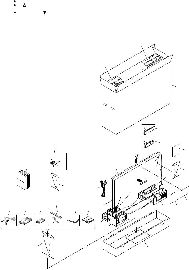
2.1 PACKING SECTION
22
B
21
27
C
|
|
|
|
|
4 |
|
|
|
|
|
|
3 |
|
|
|
|
|
|
6 |
|
|
|
|
|
|
5 |
|
|
|
|
9 |
|
|
17 |
|
|
|
|
|
|
|
D |
|
|
Noise filter |
|
|
|
|
|
for antenna cable |
|
|
|
|
|
13, 15, 18 |
|
Binder for noise filter |
|
28 |
|
|
|
|
|
20 |
||
|
|
|
|
|
|
|
|
|
|
|
|
25 |
|
|
|
|
29 |
|
1 |
|
|
|
|
|
|
|
|
|
|
|
10 |
|
|
14 |
E |
7 |
8 |
|
11 |
24 |
16 |
2 |
Speed clamp ×3 |
12 |
|
|||
|
|
|
Bead band ×3 |
|
25 |
|
|
|
|
|
|
23 |
|
19
26
F
10 |
PDP-5071PU |
1 |
2 |
3 |
4 |
|
|
5 |
6 |
(1) PACKING PARTS LIST |
|
||
Mark No. |
Description |
Part No. |
|
> |
1 |
Power Cord (2 m) |
ADG1215 |
|
2 |
G-LINK Cable (3 m) |
VDX1010 |
|
3 |
Remote Control Unit |
AXD1536 |
|
4 |
Battery Cover |
AZN2680 |
|
5 |
Simpled Remote Control Unit |
See Contrast table (2) |
|
6 |
Battery Cover |
See Contrast table (2) |
NSP 7 |
Alkaline Dry Cell Battery (LR6, AA) VEM1023 |
||
NSP |
8 |
Dry Cell Battery (R03, AAA) |
See Contrast table (2) |
|
9 |
Filter |
CTX1054 |
|
10 |
Binder Assy |
AEC1908 |
NSP 11 |
Hexagonal Wrench (6 mm) |
AEF1029 |
|
|
12 |
Cleaning Cloth |
AED1285 |
|
13 |
Operating Instructions |
ARE1426 |
|
|
(English, French, Spanish) |
|
|
14 |
Caution Card |
ARM1239 |
|
15 |
Cleaning Caution (U) |
ARM1303 |
7 8
Mark No. |
Description |
Part No. |
|
16 |
Accessory Caution |
ARM1304 |
A |
NSP 17 |
Warranty Card |
ARY1196 |
|
NSP 18 |
Card (Register) |
ARY1156 |
|
19 |
Polyethlene Bag |
AHG1394 |
|
20 |
Vinyl Bag |
AHG1347 |
|
21 |
Pad (507REG. T-L) |
AHA2571 |
|
22 |
Pad (507REG. T-R) |
AHA2572 |
|
23 |
Pad (507REG. B-L) |
AHA2573 |
|
24 |
Pad (507REG. B-R) |
AHA2574 |
|
25 |
Pad (507EL. B-ACC.) |
AHA2575 |
|
|
|
|
B |
26 |
Under Carton (507REG) |
AHD3484 |
|
27 |
Upper Carton (507REG) |
See Contrast table (2) |
|
28 |
Packing Sheet L |
AHG1389 |
|
29 |
Polyethylene Bag S |
AHG1395 |
|
C
(2) CONTRAST TABLE
PDP-5071PU/KUCXC and PDP-5070PU/KUCXC are constructed the same except for the following:
Mark |
No. |
Symbol and Description |
PDP-5071PU |
PDP-5070PU |
|
/KUCXC |
/KUCXC |
||||
|
|
|
|||
|
|
|
|
|
|
|
5 |
Simpled Remote Control Unit |
AXD1539 |
Not used |
|
|
6 |
Battery Cover |
AZN2682 |
Not used |
|
NSP |
8 |
Dry Cell Battery (R03, AAA) |
VEM1036 |
Not used |
|
|
27 |
Upper Carton |
AHD3485 |
AHD3523 |
|
|
|
|
|
|
D
E
F
|
|
|
|
|
|
11 |
|
|
PDP-5071PU |
7 |
|||
|
|
|
||||
5 |
6 |
|
|
|
8 |
|

1 |
2 |
3 |
2.2 REAR SECTION
A
36
36
B
29
C
36
MAIN
CN4010
D
E
24
36
39
F
15 |
18 |
40 |
36 |
|
20 |
||
|
|
|
|
33 |
|
|
17 |
23 |
|
22 |
|
|
34 |
|
|
36 |
26 |
|
|
37 |
1 |
36 |
28 |
38 |
|
38 |
|
13 |
36 |
|
|
6 |
|
|
8 |
|
12 |
11
MAIN
USB
11
7
2
9 A
39
36
39 36
36
36
25
15
19
36
36
14
4
10
 38 16 5
38 |
36 |
39
36
A 
TANSHI
CN8801
12 |
PDP-5071PU |
4
4040
33
31
18
30
27
36
Refer to
"2.3 FRONT SECTION".
1 |
2 |
3 |
4 |

|
5 |
6 |
(1) REAR SECTION PARTS LIST |
|
|
Mark No. |
Description |
Part No. |
1 |
SIDE KEY Assy |
AWW1133 |
2 |
SIDE Assy |
AWW1157 |
3 |
• • • • • |
|
4 |
USB Cable 120 cm (J301) |
ADF1034 |
5 |
Side Input Panel (U) |
ANC2392 |
6 |
Function Button Base |
ANG2923 |
7 |
Side Input Shield |
ANK1834 |
8 |
Function Button Shield |
ANK1835 |
NSP 9 |
PCB Support |
AEC1288 |
10 |
PCB Spacer |
AEC1570 |
11 |
Wire Saddle |
AEC1745 |
12 |
Re-use Wire Saddle |
AEC1945 |
13 |
Locking Card Spacer |
AEC2019 |
14 |
USB Spacer |
AED1310 |
15 |
Inner Grip Assy |
AMR3434 |
16 |
Gasket (USB) |
ANK1846 |
NSP 17 |
Name Label (507PU) |
See Contrast table (2) |
18 |
Side Spacer 507 |
AED1311 |
19 |
Bolt Caution Label |
AAX3075 |
NSP 20 |
Serial Seal |
AAX3182 |
7 8
Mark No. |
Description |
Part No. |
|
21 |
Side Spacer 507 |
AED1311 |
|
22 |
Terminal Display Label A (U/B) |
AAX3325 |
A |
23 |
Terminal Display Label C (U/B) |
AAX3330 |
|
24 |
Terminal Display Label B50 (U/B) |
AAX3414 |
|
25 |
Terminal Panel B (50U) |
ANC2409 |
|
26 |
Function Button Panel |
AMB2906 |
|
27 |
Side Input Cover |
AMB2911 |
|
28 |
Function Button |
AAC1562 |
|
29 |
Function Button Sheet (U) |
AAK2895 |
|
30 |
Input Cover Label U |
AAX3363 |
|
31 |
Rear Case (507) |
ANE1656 |
B |
32 |
• • • • • |
|
|
33 |
Screw (3 x 40P) |
ABA1332 |
|
34 |
Screw |
ABA1341 |
|
35 |
• • • • • |
|
|
36 |
Screw |
AMZ30P060FTB |
|
37 |
Screw |
AMZ30P080FTC |
|
38 |
Screw |
APZ30P080FTB |
|
39 |
Screw |
BPZ30P080FTB |
|
40 |
Screw |
TBZ40P080FTB |
C |
|
|
|
(2) CONTRAST TABLE
PDP-5071PU/KUCXC and PDP-5070PU/KUCXC are constructed the same except for the following:
Mark |
No. |
|
Symbol and Description |
PDP-5071PU |
PDP-5070PU |
|
/KUCXC |
/KUCXC |
|||
|
|
|
|
||
|
|
|
|
|
|
NSP |
17 |
Name Label |
|
AAL2766 |
AAL2810 |
|
|
|
|
|
|
D
E
F
|
|
|
|
|
|
13 |
|
|
PDP-5071PU |
7 |
|||
|
|
|
||||
5 |
6 |
|
|
|
8 |
|
1 |
2 |
3 |
4 |
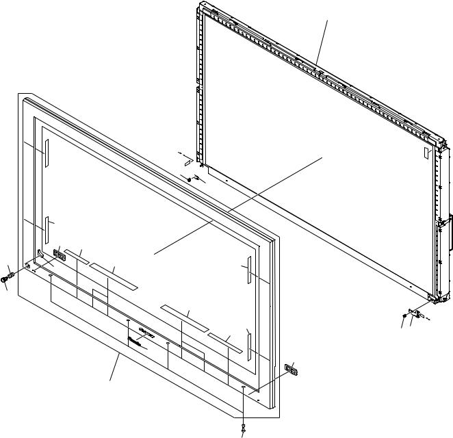
2.3 FRONT SECTION
A
Refer to
"2.4 CHASSIS SECTION (1)".
B
C
MAIN
CN4006
 10
10
8 

1
10
7 11
D |
6 |
10 |
10 |
|
|||
|
|
4 |
|
12
10
10 |
|
|
MAIN |
|
2 |
CN4010, |
|
11 |
8 |
CN4006 |
|
|
5
7
E
3
9
F
14 |
PDP-5071PU |
1 |
2 |
3 |
4 |

|
5 |
6 |
7 |
8 |
(1) FRONT SECTION PARTS LIST |
|
|
|
|
Mark No. |
Description |
Part No. |
|
|
1 |
50 LED Assy |
AWW1135 |
|
|
2 |
LED IR Assy |
AWW1136 |
|
|
3 |
Front Case Assy (507PU) |
AMB2917 |
|
|
4 |
Corner Cushion |
AEB1416 |
|
|
5 |
Pioneer Name Plate |
AAM1098 |
|
|
6 |
Coil Spring |
ABH1120 |
|
|
7 |
Blind Cushion |
AEB1415 |
|
|
8 |
Nyron Rivet |
AEC1671 |
|
|
9 |
Screw Rivet |
AEC1877 |
|
|
10 |
Insulation Sheet A |
AED1283 |
|
|
11 |
Insulation Sheet B |
AED1284 |
|
|
12 |
Power Button |
AAD4133 |
|
|
A
B
C
D
E
F
|
|
|
|
|
|
15 |
|
|
PDP-5071PU |
7 |
|||
|
|
|
||||
5 |
6 |
|
|
|
8 |
|
1 |
2 |
3 |
4 |
2.4 CHASSIS SECTION (1/2)
A
B
C
|
|
11 |
D |
22 |
21 |
|
||
|
24 |
5 |
|
|
22
16
E
23
F
16
23
Refer to
"2.7 MULTI BASE SECTION".
|
28 |
|
23 |
23 |
28 |
|
|
27 |
|
|
|
|
23 |
|
|
|
17 |
|
|
|
|
27 |
|
|
|
|
|
|
8 |
|
27 |
|
|
|
|
|
|
17 |
|
|
|
7 |
27 |
|
|
|
|
|
|
|
|
|
|
21 |
17 |
|
22 |
|
|
|
|
21 |
22 |
13 |
19 |
|
|
|
|||
12 |
22 |
|
|
|
|
15 |
|
|
|
21 |
14 |
15 |
3 |
|
|
15 |
|||
|
|
|
||
|
|
14 |
|
MAIN |
|
|
|
CN4009 |
|
|
|
|
15 |
10 |
|
|
|
25 |
|
Cleaning liquid : GEM1004
Cleaning paper : GED-008
10
21
6
25
21
9 |
|
|
|
|
2 |
22 |
|
|
|
|
|
||
|
|
24 |
|
18 |
|
11 |
|
|
21 |
|
|
||
23 |
|
|
|
|
|
|
|
|
|
|
|
|
|
|
|
POWER |
|
|
|
12 |
16 |
|
P10 |
|
|
|
|
|
POWER |
|
|
|
|
|
|
22 |
|
|
|
|
|
|
P3 |
|
|
|
|
|
|
|
|
|
|
|
|
|
|
AC inlet |
1 |
|
|
22 |
|
|
|
|
|
4 26
Refer to
"2.5 CHASSIS SECTION (2)".
PDP-5071PU
1 |
2 |
3 |
4 |

|
5 |
6 |
7 |
8 |
CHASSIS SECTION (1/2) PARTS LIST |
|
|
||
Mark No. |
Description |
Part No. |
|
|
> 1 |
Power Switch (S1) |
ASG1092 |
|
|
2 |
Ferrite Core |
ATX1044 |
|
|
3 |
Fan Motor 80 x 25L |
AXM1058 |
|
|
4 |
Housing Wire (J103) |
ADX3352 |
|
|
5 |
Front Chassis VL (50) |
AMA1014 |
|
|
6 |
Front Chassis VR (507) |
AMA1022 |
|
|
7 |
Sub Frame L Assy 507 |
ANA1945 |
|
|
8 |
Sub Frame R Assy 507 |
ANA1946 |
|
|
9 |
Front Chassis H Assy (507) |
ANA2031 |
|
|
10 |
Panel Holder H (50) |
ANG2769 |
|
|
11 |
Panel Holder V1 (50) |
ANG2770 |
|
|
12 |
Panel Holder V2 (50) |
ANG2771 |
|
|
13 |
Fan Holder |
ANG2833 |
|
|
14 |
Multi Base Holder |
ANG2937 |
|
|
15 |
Floating Rubber 80 |
AEB1427 |
|
|
16 |
PCB Spacer |
AEC1570 |
|
|
17 |
Wire Saddle |
AEC1745 |
|
|
18 |
Ferrite Core Holder |
AEC1818 |
|
|
19 |
Re-use Wire Saddle |
AEC1945 |
|
|
20 |
• • • • • |
|
|
|
21 |
Screw |
ABA1313 |
|
|
22 |
Screw |
ABZ30P080FTC |
|
|
23 |
Screw |
AMZ30P060FTB |
|
|
24 |
Screw |
APZ30P080FTB |
|
|
25 |
Screw |
BBZ30P060FTC |
|
|
26 |
Screw |
BPZ30P080FTB |
|
|
27 |
Screw |
TBZ40P080FTB |
|
|
28 |
Screw |
ABA1364 |
|
|
A
B
C
D
E
F
|
|
|
|
|
|
17 |
|
|
PDP-5071PU |
7 |
|||
|
|
|
||||
5 |
6 |
|
|
|
8 |
|
1 |
2 |
3 |
4 |
2.5 CHASSIS SECTION (2/2)
A
9 |
28 |
20 |
B
C
23
47
I
3 32
D |
21 |
|
|
|
22 |
27
30
I
L
E
43 |
M |
|
|
32 |
|
|
32 |
|
|
28 H |
10 |
|
|
|
12 |
28 |
A 8, 31 |
MAIN |
|
|
CN4001 |
|
|
B |
8, 31 |
J
|
L M |
17 |
47 |
|
|
||
|
|
|
|
|
46 |
|
46 |
|
|
4 |
|
|
|
|
|
46 |
|
|
33 |
|
|
|
|
|
|
|
K |
|
|
|
H 32 |
|
|
32 |
40 |
|
32 |
|
|
41 |
|
|
|
|
|
|
|
|
|
27 |
32 |
27 |
36 |
|
28 |
|
29 |
|
|
35 |
|
||
47 |
|
|
|
47 |
|
|
|
 A
A
B
43
43 |
C |
|
|
G |
F |
19 |
|
|
|
|
|
|
|
|
|
|
|
|
||
|
|
|
5 |
|
|
|
|
|
|
|
|
32 |
|
11 |
|
|
|
|
|
|
|
|
|
|
|
|
32 |
|
|
34 |
|
|
|
|
|
|
|
|
28 |
|
|
|
|
|
14 |
|
|
|
|
28 |
|
|
|
|
|
|
|
|
E |
|
|
|
|
8, 31 |
28 |
|
|
|
|
||
C |
8, 31 |
|
|
13 |
|
|
|
|
|
AUDIO |
|
28 |
|
|
|
|
|
|
|
D |
|
|
|
|
|
|
|
CN3751 |
|
8, 31 |
|
|
|
||
|
|
|
|
|
|
|
||
|
J |
|
15 |
MAIN |
|
|
|
|
|
F K |
|
|
|
|
|||
MAIN |
|
|
CN4002 |
|
|
|
||
CN4008 |
46 |
|
|
46 |
|
|
|
|
|
|
|
|
|
|
|
||
|
|
|
|
|
|
7 |
|
|
|
|
|
|
|
|
|
|
16 |
Power |
|
|
|
AC inlet |
|
|
||
switch |
32 |
|
|
|
||||
|
|
|
|
|
||||
46 |
|
|
|
|
|
|
||
32 |
|
|
|
|
1 |
|
47 |
|
|
|
|
|
42 |
46 |
|||
|
|
|
32 |
|
32 |
46 |
||
|
|
|
|
|
|
|
46 47 |
|
|
|
|
|
32 |
|
E |
|
|
|
|
|
|
|
|
|
|
|
|
|
|
32 |
|
|
O |
|
|
32 |
44 |
|
|
|
|
N |
|
|
|
|
|
|
|
|
|
||
|
|
|
|
37 |
44 |
18 |
|
|
|
|
|
|
|
|
|
||
|
32 |
32 |
|
|
|
|
|
|
|
|
|
|
|
32 |
|
32 |
|
|
|
|
|
|
|
|
||
|
G |
|
|
|
|
|
|
|
|
|
39 |
|
|
32 |
|
32 |
|
26 |
|
|
27 |
|
|
|||
|
|
|
|
|
|
32 |
32 |
|
|
|
|
6 |
|
|
|
||
|
|
|
|
|
|
|
||
29 |
|
|
|
|
32 |
|
||
|
|
|
|
|
|
|
||
38
25
27
32 |
32 |
|
|
|
|
|
N |
|
32 |
30 |
47 |
|
|
|
|
||
43 |
32 |
|
|
|
|
|
|
D |
|
||
|
43 |
43 |
|
O |
|
|
|
|
|
||
F |
|
|
|
|
|
|
|
|
30 |
|
|
|
|
|
|
|
|
|
|
|
|
47 |
Refer to |
|
|
|
|
|
|
|
|
|
|
|
"2.6 PANEL CHASSIS SECTION". |
18 |
|
|
|
PDP-5071PU |
|
2
24
1 |
2 |
3 |
4 |

|
5 |
6 |
7 |
8 |
CHASSIS SECTION (2/2) PARTS LIST |
|
|
||
Mark No. |
Description |
Part No. |
|
|
1 |
50 X MAIN DRIVE Assy |
AWW1143 |
|
|
2 |
50 X SUB DRIVE Assy |
AWW1144 |
|
A |
3 |
50 Y MAIN DRIVE Assy |
AWW1145 |
|
|
4 |
50 Y SUB DRIVE Assy |
AWW1146 |
|
|
5 |
50 DIGITAL Assy |
AWW1139 |
|
|
6 |
SENSOR Assy |
AWW1140 |
|
|
> 7 |
POWER SUPPLY Unit |
AXY1153 |
|
|
8 |
Ferrite Core |
ATX1048 |
|
|
9 |
Flexible Cable (J201) |
ADD1435 |
|
|
10 |
Flexible Cable (J202) |
ADD1436 |
|
|
11 |
Flexible Cable (J206) |
ADD1440 |
|
B |
|
|
|||
12 |
Flexible Cable (J203) |
ADD1463 |
|
|
13 |
Flexible Cable (J205) |
ADD1465 |
|
|
14 |
Flexible Cable (J204) |
ADD1466 |
|
|
15 |
9P&6/5P Housing Wire (J101) |
ADX3337 |
|
|
16 |
8P&5P Housing Wire (J102) |
ADX3338 |
17 |
8P/4P Housing Wire (J108) |
ADX3339 |
18 |
8P/4P Housing Wire (J109) |
ADX3340 |
19 |
14P Housing Wire (J105) |
ADX3354 |
20 |
5P Housing Wire (J110) |
ADX3359 |
21 |
10P Housing Wire (J122) |
ADX3300 |
22 |
4P Housing Wire (J119) |
ADX3346 |
23 |
Conductive Plate Y |
ANG2902 |
24 |
Conductive Plate X |
ANG2905 |
25 |
Cushion |
AEB1424 |
26 |
Nyron Rivet |
AEC1671 |
27 |
Wire Saddle |
AEC1745 |
28 |
Flat Clamp |
AEC1879 |
29 |
PCB Support |
AEC1938 |
30 |
Harness Lifter 28 |
AEC1982 |
31 |
Ferrite Clamp |
AEC1986 |
32 |
Re-use PCB Spacer |
AEC2087 |
33 |
Tapping Card Spacer |
AEC2103 |
34 |
Flat Clamp 60 |
AEC2104 |
35 |
Drive Silicone Sheet B |
AEH1109 |
36 |
Drive Silicone Sheet C |
AEH1110 |
37 |
Power Supply Sheet B (507) |
AMR3555 |
38 |
Address Sheet A |
AMR3628 |
39 |
Address Sheet B |
AMR3629 |
40 |
Address Sheet E |
AMR3645 |
41 |
Address Sheet F |
AMR3646 |
42 |
Power Supply Sheet (507) |
AMR3634 |
43 |
Gasket AV8 |
ANK1881 |
44 |
Rivet A |
BEC1158 |
45 |
• • • • • |
|
46 |
Screw |
ABA1313 |
47 |
Screw |
ABA1364 |
|
|
|
|
|
|
19 |
|
|
PDP-5071PU |
7 |
|||
|
|
|
||||
5 |
6 |
|
|
|
8 |
|
C
D
E
F
1 |
2 |
3 |
4 |
2.6 PANEL CHASSIS SECTION
A
B
6
1 7
5
7
C |
7 |
7
10
9
|
7 |
|
|
|
|
3 |
10 |
|
|
D |
7 |
|
|
|
|
|
|
||
|
|
7 |
|
|
|
|
4 |
7 |
2 |
|
|
|
||
|
|
|
|
11 |
E |
|
|
|
8 |
F
20 |
PDP-5071PU |
1 |
2 |
3 |
4 |
|
5 |
6 |
7 |
8 |
PANEL CHASSIS SECTION PARTS LIST |
|
|
||
Mark No. |
Description |
Part No. |
|
|
NSP 1 |
Panel Chassis (507) Assy |
AWU1148 |
|
|
NSP 2 |
Plasma Panel (50DC) Assy |
AWU1162 |
|
|
NSP 3 |
50 ADDRESS L Assy |
AWW1141 |
|
|
NSP 4 |
50 ADDRESS S Assy |
AWW1142 |
|
|
NSP 5 |
50 SCAN A Assy |
AWW1147 |
|
|
NSP 6 |
50 SCAN B Assy |
AWW1148 |
|
|
7 |
Re-use PCB Spacer |
AEC2088 |
|
|
NSP 8 |
Adhesive Tape (50) |
AEH1119 |
|
|
9 |
Conductive Plate Holder |
AMR3446 |
|
|
10 |
Screw |
ABA1351 |
|
|
NSP 11 |
Tube Cover |
AMR3445 |
|
|
A
B
C
D
E
F
|
|
|
|
|
|
21 |
|
|
PDP-5071PU |
7 |
|||
|
|
|
||||
5 |
6 |
|
|
|
8 |
|

1 |
2 |
3 |
2.7 MULTIBASE SECTION
A
SIDE KEY CN9501
LED IR CN9701
20
51
31
8
B
B
C 7
1
C
D
23
E |
45 |
|
|
|
51 |
|
51 |
F 2
13 |
50 DIGITAL |
|
|
CN3001 |
|
A |
POWER |
|
51 |
||
P8 |
17 POWER
P9 |
|
44 |
|
USB |
G |
||
|
|||
(side) |
|
44 |
|
|
|
||
E |
F |
|
|
|
|
||
|
51 |
Fan |
 D
D
|
50 LED |
|
|
|
CN9651 |
7 |
|
51 |
20 |
51 |
|
|
D |
|
14 |
|
|
|
|
48 |
|
|
|
48 |
32 |
|
|
46 |
38 |
51 |
|
46 |
|
|
37 |
|
|
|
|
4 |
47 |
49 |
|
|
|
|
|
||
|
|
35 |
|
48 |
|
|
A |
47 |
|
|
|
46 |
||
19 |
|
|
50 |
24 |
|
|
|
||
|
18 |
|
46 |
|
|
|
|
||
|
33 |
30 |
|
POWER |
|
|
P5 |
||
|
|
|
||
|
|
|
|
6 |
33 |
|
|
|
|
5 |
|
|
|
27 |
|
|
|
|
|
|
|
|
|
26 |
|
|
|
25 |
|
45 |
|
30 |
|
|
|
|
|
|
|
11
B 
C 
12
30
 SIDE
SIDE
CN9101
22
22 |
PDP-5071PU |
4
43
51
51
|
39 |
|
3 |
|
15 |
|
F |
31 |
E |
|
15 |
51 |
7 |
POWER
P3
21
10
46
52
28
30 26
25 |
9 |
16 |
G |
|
29
36
1 |
2 |
3 |
4 |

|
|
5 |
6 |
MULTIBASE SECTION PARTS LIST |
|||
Mark No. |
Description |
Part No. |
|
|
1 |
MAIN Assy |
AWV2312 |
|
2 |
TANSHI Assy |
AWW1156 |
|
3 |
POD Assy |
AWW1154 |
|
4 |
AUDIO Assy |
AWW1131 |
|
5 |
SP TERMINAL Assy |
AWW1132 |
|
6 |
Ferrite Core |
ATX1044 |
|
7 |
Ferrite Core |
ATX1048 |
|
8 |
Ferrite Core |
ATX1064 |
> |
9 |
Power Switch (S2)(TRAP) |
ASG1089 |
> |
10 |
AC Inlet (CN1) |
AKP1301 |
|
11 |
Flexible Cable (J210) |
ADD1441 |
|
12 |
Flexible Cable (J211) |
ADD1442 |
|
13 |
Flexible Cable (J207) |
ADD1445 |
|
14 |
Flexible Cable (J213) |
ADD1446 |
|
15 |
Flexible Cable (J214)(J215) |
ADD1447 |
|
16 |
3P Housing Wire (J121) |
ADX3348 |
|
17 |
13P&11P Housing Wire (J106) |
ADX3355 |
|
18 |
3P Housing Wire (J107) |
ADX3356 |
|
19 |
11P Housing Wire (J111) |
ADX3360 |
|
20 |
7/6/4/3P Housing Wire (J113) |
ADX3341 |
|
21 |
Housing Wire (J104) |
ADX3353 |
|
22 |
14P Housing Wire (J116) |
ADX3344 |
|
23 |
8/4P Housing Wire (J117) |
ADX3345 |
|
24 |
Binder |
AEC-093 |
|
25 |
Locking Card Spacer |
AEC1429 |
|
26 |
Wire Saddle |
AEC1745 |
|
27 |
Ferrite Core Holder |
AEC1818 |
|
28 |
Clamp |
AEC1884 |
|
29 |
Card Spacer |
AEC1889 |
|
30 |
Re-use Wire Saddle |
AEC1945 |
|
31 |
Ferrite Stopper |
AEC1981 |
|
32 |
Ferrite Clamp |
AEC1986 |
|
33 |
Locking Card Spacer |
AEC2019 |
|
34 |
• • • • • |
|
|
35 |
POD Cover |
AMR3542 |
|
36 |
Multi Base (U) Assy |
ANA1951 |
|
37 |
Terminal Panel A (U/B) |
ANC2394 |
|
38 |
POD Stay A |
ANG2933 |
|
39 |
Tuner Stay U |
ANG3028 |
|
40 |
• • • • • |
|
|
7 |
8 |
Mark No. |
Description |
Part No. |
41• • • • •
42• • • • •
> 43 |
Gasket UB |
ANK1867 |
44 |
Tuner Shield |
ANK1875 |
45 |
Locking Card Spacer |
AEC2093 |
46 |
Screw |
AMZ30P060FTB |
47 |
Hex. Head Screw |
BBA1051 |
48 |
Nut |
BBN1005 |
49 |
Screw |
BMZ30P060FTB |
50 |
Screw |
BPZ30P080FTB |
51 |
Screw |
PMB30P080FNI |
52 |
Inlet Spacer |
AEC2112 |
A
B
C
D
E
F
|
|
|
|
|
|
23 |
|
|
PDP-5071PU |
7 |
|||
|
|
|
||||
5 |
6 |
|
|
|
8 |
|
1 |
2 |
3 |
4 |
2.8 PDP SERVICE ASSY 507 (AWU1212)
A |
36 ×4 |
35 ×2 |
Note: |
||
The parts labeled here with circled numbers |
32 |
|
are supplied with the Assy for service. |
|
|
|
|
|
Attach them, referring to this diagram. |
×2 |
|
35 |
|
B
C
D
48 |
33 |
×5 |
|
47
11
E
6
4
36
21
18
12
|
33 |
2 |
15 |
|
|
33 |
|
|
12 ×2 |
17 |
|
|
18 ×3 |
33 ×4
26
26
35
26
33 ×4
35
36
36
33 |
12 ×2 |
17 ×2
15
26
26
26
18 ×3
33 ×5
17
48
11
35 ×2
36
5
27
27
20
18
34 ×4
Re-use PCB Spacer
This spacer is used for attaching the Gasket AV8, and is not included in the Assy
Ffor service. Remove the 6 PCB Spacers from the product to be repaired and attach them to the Assy for service.
24
47
14 ×4
PDP-5071PU
35 ×2
36 ×4
36 ×4
32
29
Power supply sheet B (507)
This is not included in the Assy for service. Detach it from the product to be repaired and attach it to the Assy for service.
7
19
19
9
12 ×5
1
33
34 ×4 
33
 3 33
3 33
28
(for transport)
1 |
2 |
3 |
4 |
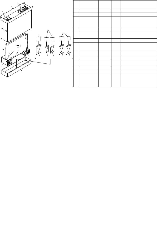
5 6 7 8
 Packing Section
41 |
|
|
|
|
(*) No. |
Part Name |
Part No. |
No. of |
Remarks |
|
45 |
|
|
|
|
|
|||||
|
|
|
|
pcs |
|
|||||
|
|
|
|
|
|
|
|
|
|
|
40 |
|
|
|
|
8 |
Clamp base |
ANG3030 |
×1 |
Not used |
A |
|
|
|
|
|
10 |
PCB spacer |
AEC1126 |
×4 |
Not used |
|
|
|
10 ×4, 11 ×2, 12 ×11, |
|
|
|
|
Ten of the 11 wire saddles are to be used |
|
||
|
|
13 ×9, 15 ×2, 16 ×2, |
12 |
Wire saddle |
AEC1745 |
×11 |
with this unit. Attach them to the places |
|
||
|
|
17 ×4, 18 ×10, 25 ×2, |
|
|
|
|
where T indications are engraved. |
|
||
|
|
26 ×6, 27 ×2, 36 ×1 |
13 |
Wire saddle |
AEC1751 |
×9 |
Not used |
|
||
|
|
|
|
|
|
|||||
|
8 |
|
|
20 to 24 |
|
|
|
Attach them to the places where C |
|
|
|
|
|
|
15 |
PCB support |
AEC1938 |
×2 |
|
||
|
|
|
|
|
indications are engraved. |
|
||||
|
|
|
|
|
|
|
|
|
|
|
|
|
|
|
|
16 |
PCB support |
AEC1958 |
×2 |
Not used |
|
|
|
|
|
|
17 |
Harness lifter 28 |
AEC1982 |
×4 |
Attach them to the places where U |
|
46 |
|
|
|
|
indications are engraved. |
|
||||
|
|
|
|
|
|
|
|
|
||
|
|
|
|
|
|
|
|
|
B |
|
|
|
|
|
|
18 |
Ferrite clamp |
AEC1986 |
×10 |
Eight of the 10 ferrite clamps are to be |
|
|
|
|
|
|
used with this unit. |
|
||||
43 |
37 |
38 |
38 |
39 |
39 |
|
|
|
|
|
DC sheet A |
AMR3612 |
×1 |
Not used |
|
||||||
|
|
|
|
|
22 |
|
||||
42 |
|
|
|
|
23 |
Address sheet E |
AMR3621 |
×1 |
Not used |
|
|
|
|
|
24 |
Address sheet D |
AMR3631 |
×1 |
Not used |
|
|
|
|
|
|
|
|
|||||
44 |
|
|
|
|
25 |
Gasket E |
ANK1874 |
×2 |
Not used |
|
|
|
|
|
|
|
|
|
Twelve screws have been already |
|
|
|
|
|
|
|
|
|
|
|
|
|
|
|
|
|
|
36 |
Screw |
TBZ40P080FTB |
×13 |
secured to the Assy. |
|
|
|
|
|
|
The remaining one screw packed in a |
|
||||
|
|
|
|
|
|
|
|
|
|
|
|
|
|
|
|
|
|
|
|
plastic bag is not used with this unit. |
|
PDP SERVICE ASSY 507 (AWU1212) PARTS LIST
Mark No. |
Description |
Part No. |
Mark No. |
Description |
Part No. |
NSP 1 |
Panel Chassis (507) Assy |
AWU1148 |
26 |
Gasket AV8 |
ANK1881 |
2 |
Front Chassis VL (50) |
AMA1014 |
27 |
Rivet A |
BEC1158 |
3 |
Front Chassis VR (507) |
AMA1022 |
NSP 28 |
Front Case Assy (507SV) |
AMB2977 |
4 |
Sub Frame L Assy 507 |
ANA1945 |
29 |
Rear Case (507) |
ANE1656 |
5 |
Sub Frame R Assy 507 |
ANA1946 |
30 |
Caution Label |
AAX3031 |
6 |
Front Chassis H Assy (507) |
ANA2031 |
NSP 31 |
Drive Voltage Label |
ARW1097 |
7 |
Conductive Plate X |
ANG2905 |
32 |
Screw (3 x 40P) |
ABA1332 |
8 |
Clamp Base (*) |
ANG3030 |
33 |
Screw |
ABA1351 |
9 |
Cushion |
AEB1424 |
34 |
Screw |
ABA1364 |
NSP 10 |
PCB Spacer (*) |
AEC1126 |
35 |
Screw |
AMZ30P060FTB |
11 |
PCB Spacer |
AEC1570 |
36 |
Screw (*) |
TBZ40P080FTB |
12 |
Wire Saddle (*) |
AEC1745 |
37 |
Polyethylene Bag |
AHG1337 |
13 |
Wire Saddle (*) |
AEC1751 |
38 |
Polyethylene Bag S |
AHG1338 |
14 |
Screw Rivet |
AEC1877 |
39 |
Polyethylene Bag |
AHG1340 |
15 |
PCB Support (*) |
AEC1938 |
40 |
Pad (507 T-L) |
AHA2538 |
16 |
PCB Support (*) |
AEC1958 |
41 |
Pad (507 T-R) |
AHA2539 |
17 |
Harness Lifter 28 (*) |
AEC1982 |
42 |
Pad (507 B-L) |
AHA2540 |
18 |
Ferrite Clamp (*) |
AEC1986 |
43 |
Pad (507 B-R) |
AHA2541 |
19 |
Re-use PCB Spacer |
AEC2087 |
44 |
Under Carton (507) |
AHD3473 |
20 |
Address Sheet A |
AMR3628 |
45 |
Upper Carton (507SV) |
AHD3550 |
21 |
Address Sheet F |
AMR3646 |
46 |
Protect Sheet |
AHG1331 |
22 |
DC Sheet A (*) |
AMR3612 |
47 |
Screw |
ABZ30P080FTC |
23 |
Address Sheet E (*) |
AMR3621 |
48 |
Screw |
APZ30P080FTB |
24 |
Address Sheet D (*) |
AMR3631 |
|
|
|
25 |
Gasket E (*) |
ANK1874 |
|
|
|
|
|
|
|
|
|
25 |
|
|
PDP-5071PU |
7 |
|||
|
|
|
||||
5 |
6 |
|
|
|
8 |
|
C
D
E
F
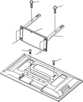
1 |
2 |
3 |
4 |
2.9 TABLE TOP STAND |
|
|
|
|
|
4 |
|
A |
|
|
4 |
2
1
B |
5 |
|
3
5
3
C
D
TABLE TOP STAND PARTS LIST
Mark No. |
Description |
Part No. |
NSP 1 |
Stand Pipe Assy |
AXY1141 |
NSP 2 |
Base Cover Assy |
AXY1142 |
3 |
Bolt (HEX) |
ABA1358 |
4 |
Bolt (HEX) |
ABA1359 |
5 |
Screw |
ABA1360 |
E
F
26 |
PDP-5071PU |
1 |
2 |
3 |
4 |

5 |
6 |
7 |
8 |
3. PCB PARTS LIST |
|
|
|
NOTES: Parts marked by "NSP" are generally unavailable because they are not in our Master Spare Parts List. |
|
||
The |
mark found on some component parts indicates the importance of the safety factor of the part. |
|
|
Therefore, when replacing, be sure to use parts of identical designation.
|
When ordering resistors, first convert |
resistance values into code form as shown in the following examples. |
|||||||||
|
Ex.1 When there are 2 effective digits (any digit apart from 0), such as 560 ohm and 47k ohm (tolerance is shown by J=5%, |
||||||||||
|
and K=10%). |
|
|
|
|
|
|
|
|
||
|
560 Ω |
|
|
56 x 10 1 |
|
561 |
|
|
RD1/4PU 5 6 1 J |
|
|
|
|
|
|
|
|
||||||
|
47k Ω |
|
|
47 x 10 3 |
|
473 |
|
|
RD1/4PU 4 7 3 J |
|
|
|
|
|
|
|
|
|
|||||
|
0.5 Ω |
|
|
R50 |
|
|
|
RN2H R 5 0 K |
|
||
|
|
|
|
|
|
||||||
|
1 Ω |
|
|
1R0 |
|
|
|
RS1P 1 R 0 K |
|
||
|
|
|
|
|
|
||||||
|
Ex.2 When there are 3 effective digits (such as in high precision metal film resistors). |
|
|||||||||
|
5.62k Ω |
|
|
562 x 10 1 |
|
5621 |
|
|
RN1/4PC 5 6 2 1 F |
|
|
|
|
|
|
|
|
||||||
Mark No. |
Description |
Part No. |
Mark No. |
Description |
Part No. |
||||||
|
|
|
|
|
|
|
|
|
|
|
|
LIST OF ASSEMBLIES
NSP |
1..PANEL CHASSIS (507) ASSY |
AWU1148 |
NSP |
2..50 ADDRESS ASSY |
AWV2303 |
NSP |
3..50 ADDRESS L ASSY |
AWW1141 |
NSP |
3..50 ADDRESS S ASSY |
AWW1142 |
NSP |
2..50 SCAN ASSY |
AWV2304 |
NSP |
3..50 SCAN A ASSY |
AWW1147 |
NSP |
3..50 SCAN B ASSY |
AWW1148 |
NSP |
1..50 X DRIVE ASSY |
AWV2305 |
|
2..50 X MAIN DRIVE ASSY |
AWW1143 |
|
2..50 X SUB DRIVE ASSY |
AWW1144 |
NSP |
1..50 Y DRIVE ASSY |
AWV2306 |
|
2..50 Y MAIN DRIVE ASSY |
AWW1145 |
|
2..50 Y SUB DRIVE ASSY |
AWW1146 |
NSP |
1..50 DIGITAL ASSY |
AWV2302 |
|
2..50 DIGITAL ASSY |
AWW1139 |
|
2..SENSOR ASSY |
AWW1140 |
|
1..MAIN ASSY (US BB) |
AWV2312 |
NSP |
1..I/O ASSY |
AWV2313 |
|
2..POD ASSY |
AWW1154 |
|
2..TANSHI ASSY |
AWW1156 |
|
2..SIDE ASSY |
AWW1157 |
NSP |
1..50 AUDIO FUKUGO ASSY |
AWV2346 |
|
2..AUDIO ASSY |
AWW1131 |
|
2..SP TERMINAL ASSY |
AWW1132 |
|
2..SIDE KEY ASSY |
AWW1133 |
|
2..50 LED ASSY |
AWW1135 |
|
2..LED IR ASSY |
AWW1136 |
> |
1..POWER SUPPLY UNIT |
AXY1153 |
Mark No. Description Part No.
50 DIGITAL ASSY
[DIGITAL IF BLOCK]
MISCELLANEOUS
F3001 |
|
CCG1162 |
CN3001 |
50P CONNECTOR |
AKM1353 |
CN3002 |
20P FFC CONNECTOR |
AKM1235 |
[MODULE UCOM BLOCK]
SEMICONDUCTORS
IC3151 |
|
AGC1011 |
IC3152, 3153 |
SN74AHC541PW |
|
IC3155 |
|
SN74AHC08PW |
IC3156 |
|
BR24L04FJ-W |
IC3157 |
|
M62334FP |
IC3159 |
|
TC7W126FU |
IC3160, 3161 |
TC74VHC123AFTS1 |
|
Q3151 |
|
2SJ461A |
D3151, 3152, 3154, 3155 |
DAN202U |
|
D3158, 3159, 3161–3163 |
1SS355 |
|
MISCELLANEOUS |
|
|
X3151 |
|
CSS1616 |
CN3151 |
CONNECTOR |
AKM1276 |
CN3152 |
CONNECTOR |
CKS4828 |
RESISTORS |
|
|
R3155, 3160, 3170, 3176 |
RAB4C101J |
|
R3174 |
|
RAB4C103J |
Other Resistors |
RS1/16SS###J |
|
CAPACITORS |
|
|
C3151 |
|
CEHVKW470M6R3 |
C3152, 3153, 3155–3158 |
CKSSYB104K10 |
|
C3159, 3171, 3172, 3182 |
CKSRYB105K6R3 |
|
C3162, 3163, 3165, 3166 |
CKSSYB104K10 |
|
C3164 |
|
CCSSCH101J50 |
C3167 |
|
CKSSYB103K16 |
C3168, 3170, 3181 |
CKSSYB104K10 |
|
[PANEL FLASH BLOCK] |
|
|
SEMICONDUCTORS |
|
|
IC3301 |
|
AGC1009 |
IC3302, 3305 |
PST3628UR |
|
IC3303 |
|
SN74AHC08PW |
IC3304 |
|
PST3610UR |
Q3301 |
|
RN1901 |
Q3302 |
|
HN1C01FU |
RESISTORS |
|
|
|
MISCELLANEOUS |
|
|
|
|
|
X3302 |
|
ASS1188 |
|
R3007, 3010–3016 |
RAB4C470J |
|
|
|
||
|
|
CN3301 |
CONNECTOR |
CKS4835 |
||
R3020–3022 |
RAB4C103J |
|
|
|||
|
|
|
|
|
||
Other Resistors |
RS1/16SS###J |
|
|
RESISTORS |
|
|
|
|
|
|
|
||
|
|
|
|
R3307, 3308 |
RAB4C101J |
|
|
|
|
|
|
|
27 |
|
|
PDP-5071PU |
7 |
|||
|
|
|
||||
5 |
6 |
|
|
|
8 |
|
A
B
C
D
E
F
|
|
|
1 |
|
2 |
|
Mark No. |
Description |
Part No. |
||
|
|
|
|
|
|
|
Other Resistors |
RS1/16SS###J |
|||
A |
CAPACITORS |
|
|||
|
C3301–3303, 3306, 3308 |
CKSSYB104K10 |
|||
|
C3304, 3307, 3309 |
CKSSYB472K16 |
|||
|
C3305, 3310 |
CKSSYB102K50 |
|||
|
C3311 |
|
|
CCSRCH470J50 |
|
|
C3315, 3316 |
CKSSYB104K10 |
|||
|
C3317 |
|
|
CCSRCH471J50 |
|
|
[SQ ASIC BLOCK] |
|
|||
|
SEMICONDUCTORS |
|
|||
B |
IC3401 |
|
|
PEG239A |
|
|
|
|
|
|
|
|
MISCELLANEOUS |
|
|||
|
L3401–3403 |
QTL1013 |
|||
|
F3401, 3402 |
CCG1162 |
|||
|
RESISTORS |
|
|||
|
R3402, 3412 |
RAB4C101J |
|||
|
R3405–3407, 3409, 3410 |
RAB4C220J |
|||
|
R3416 |
|
|
RAB4C220J |
|
|
R3425 |
|
|
RS1/16SS5601F |
|
|
Other Resistors |
RS1/16SS###J |
|||
C |
CAPACITORS |
|
|||
|
C3401, 3402, 3419, 3425 |
CEHVKW101M6R3 |
|||
|
C3403–3413, 3417, 3418 |
CKSSYB104K10 |
|||
|
C3420–3424, 3426–3432 |
CKSSYB104K10 |
|||
|
C3445–3448 |
CKSSYB104K10 |
|||
|
[ADDRESS CN BLOCK] |
|
|||
|
SEMICONDUCTORS |
|
|||
|
Q3501, 3502 |
RN1901 |
|||
|
D3501, 3502 |
DAN202U |
|||
D |
MISCELLANEOUS |
|
|||
|
CN3501–3504, 3506 40P CONNECTOR |
AKM1348 |
|||
|
CN3505 |
18P CONNECTOR |
VKN1310 |
||
|
RESISTORS |
|
|||
|
R3519, 3520 |
RAB4C472J |
|||
|
R3521, 3522, 3525 |
RAB4C101J |
|||
|
R3524 |
|
|
RAB4C222J |
|
|
Other Resistors |
RS1/16SS###J |
|||
|
[DIGITAL DD CON BLOCK] |
|
|||
E |
SEMICONDUCTORS |
|
|||
IC3601 |
|
|
BA80BC0WFP |
||
|
|
|
|||
|
MISCELLANEOUS |
|
|||
|
U3601 |
DD CON UNIT |
AXY1137 |
||
|
RESISTORS |
|
|||
|
R3611 |
|
|
RAB4C101J |
|
|
Other Resistors |
RS1/16SS###J |
|||
|
CAPACITORS |
|
|||
|
C3609 |
|
|
CKSSYB104K10 |
|
F |
C3611 |
|
|
CKSQYB105K16 |
|
C3612 |
|
|
ACH1394 |
||
|
C3613 |
|
|
CKSSYB103K16 |
|
3 |
|
4 |
|
Mark No. |
Description |
Part No. |
|
|
|
|
|
SENSOR ASSY
SEMICONDUCTORS
IC3651 |
MM1522XU |
IC3652 |
BR24L02FJ-W |
Q3651 |
HN1B04FU |
MISCELLANEOUS
CN3651 CONNECTOR |
AKM1276 |
RESISTORS
Other Resistors RS1/16SS###J
CAPACITORS
C3651, 3653 |
CKSRYB105K6R3 |
C3652, 3654 |
CKSSYB103K16 |
C3656, 3657 |
CKSSYB104K10 |
50 X MAIN DRIVE ASSY
[50X LOGIC BLOCK]
SEMICONDUCTORS
IC1001 |
TC74ACT541FT |
IC1002 |
TC74VHC00FTS1 |
D1001–1004 |
1SS355 |
MISCELLANEOUS
K1004, 1007 TEST PIN |
AKX1061 |
CN1001 18P CONNECTOR |
VKN1310 |
RESISTORS
R1001, 1006 |
RAB4C470J |
R1004 |
RAB4C472J |
VR1001 |
CCP1390 |
Other Resistors |
RS1/16S###J |
CAPACITORS
C1001 |
CEHAT470M16 |
C1002, 1003 |
CKSRYB104K16 |
C1004 |
CCSRCH331J50 |
C1006 |
CCSRCH680J50 |
[50X RESONANCE BLCOK]
SEMICONDUCTORS
IC1101, 1105 |
TND307TD |
IC1102 |
PS9117P |
IC1104 |
AXF1163 |
IC1107 |
PS2701A-1(L) |
Q1101 |
2SC2412K |
Q1102, 1103 |
QSZ2 |
Q1104, 1105 |
2SC4081 |
D1101, 1103 |
UDZS5R6(B) |
D1102 |
CRH01 |
D1104 |
UDZS15(B) |
MISCELLANEOUS |
|
L1101 |
ATH1217 |
L1106 |
ATH1216 |
F1101 |
CTF1449 |
1101 |
ANH1653 |
1102 |
AEH1092 |
1103 |
BMZ30P080FTC |
28 |
PDP-5071PU |
1 |
2 |
3 |
4 |

|
|
5 |
6 |
Mark No. |
Description |
Part No. |
|
|
|
|
|
RESISTORS |
|
||
R1107, 1108 |
RS3LMF100J |
||
R1109, 1110 |
RS1/10S4702F |
||
R1113 |
|
RS1/16S1002F |
|
R1114 |
|
RS1/16S3302F |
|
R1115 |
|
ACN1259 |
|
R1119 |
|
ACN1258 |
|
R1121 |
|
RS1/16S4701F |
|
Other Resistors |
RS1/16S###J |
||
CAPACITORS |
|
||
C1101, 1114 |
CEHAT470M25 |
||
C1102, 1115 |
CKSRYF104Z50 |
||
C1103 |
|
CKSRYB104K16 |
|
C1104, 1117 |
CKSYB105K25 |
||
C1107, 1116 |
ACG1126 |
||
C1113 |
|
ACH1450 |
|
C1121–1124 |
ACE1178 |
||
[50X SUS BLOCK] |
|
||
SEMICONDUCTORS |
|
||
IC1201, 1204, 1206, 1208 |
TND307TD |
||
IC1202, 1205 |
PS9117P |
||
IC1209 |
|
MM1565AF |
|
Q1201, 1208 |
2SC2412K |
||
Q1202, 1204, 1205, 1207 |
H5N2512LS |
||
Q1209, 1212–1214 |
QSZ2 |
||
Q1210, 1211 |
FKP280AS |
||
Q1215, 1221 |
FKP300AS |
||
Q1216 |
|
DTC143EK |
|
Q1217 |
|
DTC123TKA |
|
Q1220 |
|
R5009ANJ |
|
D1201, 1205 |
UDZS5R6(B) |
||
D1202, 1203, 1206, 1211 |
CRH01 |
||
D1204 |
|
D1FL40 |
|
D1208 |
|
1SS302 |
|
D1209 |
|
UDZS16(B) |
|
D1210 |
|
1SS355 |
|
D1212 |
|
CRH01 |
|
D1213 |
|
UDZS8R2(B) |
|
MISCELLANEOUS |
|
||
L1201, 1203, 1204 |
BTH1134 |
||
L1202 |
|
ATH1186 |
|
F1227 |
|
CTF1449 |
|
K1202 |
TEST PIN |
AKX1061 |
|
KN1201–1204, 1210–1217 |
ANK1841 |
||
CN1201 |
14P CONNECTOR |
14PL-FJ |
|
CN1204 |
8P TOP POST |
B8B-EH |
|
1202 SCREW |
PMB30P080FNI |
||
RESISTORS |
|
||
R1208, 1210, 1213, 1215 |
RS1/10S100J |
||
R1211 |
|
ACN1254 |
|
R1219, 1228, 1230, 1231 |
RS1/10S0R0J |
||
R1220, 1224, 1233, 1256 |
RS1/10S2R2J |
||
R1237 |
|
RS1/10S0R0J |
|
R1239 |
|
ACN1258 |
|
R1245 |
|
ACN1257 |
|
R1247, 1248 |
RS3LMF470J |
||
Other Resistors |
RS1/16S###J |
||
|
|
5 |
6 |
7 8
|
Mark No. |
Description |
Part No. |
|
|||
|
|
|
|
|
|
|
|
|
|
CAPACITORS |
|
|
|
||
|
|
C1201, 1212 |
|
ACG1126 |
|
||
|
|
C1202, 1209, 1232, 1236 |
CKSRYB104K16 |
A |
|||
|
|
C1203, 1208, 1215, 1229 |
CKSRYF104Z50 |
||||
|
|
C1205, 1206, 1217, 1218 |
ACG1139 |
|
|||
|
|
C1207, 1214, 1220, 1226 |
CEHAT470M25 |
|
|||
|
|
C1210, 1211, 1216, 1241 |
CKSYB105K25 |
|
|||
|
|
C1213 |
|
CCSRCH221J50 |
|
||
|
|
C1222, 1223 |
|
ACH1423 |
|
||
|
|
C1224, 1225 |
|
ACE1178 |
|
||
|
|
C1228 |
|
CEHAT2R2M2E |
|
||
|
|
C1230 |
|
ACH1449 |
|
||
|
|
C1231, 1237 |
|
CEHAT101M10 |
|
||
|
|
C1233 |
|
CKSRYB473K16 |
B |
||
|
|
C1234 |
|
CEHAT470M16 |
|||
|
|
C1235 |
|
CKSRYB105K6R3 |
|
||
|
|
C1244 |
|
CKSRYB104K25 |
|
||
|
|
[DRIVE HEAT SINK M] |
|
|
|||
|
|
MISCELLANEOUS |
|
|
|||
3001, 3001 |
|
ANH1656 |
|
||||
3001 |
|
|
ANH1656 |
|
|||
3101, 3101 |
|
ANG2679 |
|
||||
3101 |
|
|
ANG2679 |
|
|||
|
|
|
|
|
|
|
C |
|
|
[50X D-D CON BLOCK] |
|
|
|||
|
|
SEMICONDUCTORS |
|
|
|||
|
|
IC1301 |
|
PS2701A-1(L) |
|
||
|
|
IC1302 |
|
TA76431FR |
|
||
|
|
Q1301 |
|
2SC2412K |
|
||
|
|
Q1303, 1306, 1307 |
HN1C01FU |
|
|||
|
|
Q1304, 1401 |
|
2SD1898 |
|
||
|
|
Q1305 |
|
2SA1037K |
|
||
|
|
Q1402 |
|
2SC4081 |
|
||
|
|
D1307 |
|
CRF03 |
|
||
|
|
D1308, 1403 |
|
UDZS5R1(B) |
D |
||
|
|
D1309, 1311, 1401, 1405 |
CRH01 |
|
|||
|
|
D1312, 1402 |
|
1SS301 |
|
||
|
|
D1313, 1318, 1404, 1406 |
1SS355 |
|
|||
|
|
D1315, 1316 |
|
UDZS4R7(B) |
|
||
|
|
MISCELLANEOUS |
|
|
|||
|
|
T1302 |
|
ATK1160 |
|
||
|
|
T1401 |
|
ATK1159 |
|
||
|
|
RESISTORS |
|
|
|
||
|
|
R1312–1314, 1317 |
RS1/10S224J |
E |
|||
|
|
R1328 |
|
RAB4C472J |
|||
|
|
|
|
||||
|
|
VR1301 |
|
CCP1392 |
|
||
|
|
Other Resistors |
|
RS1/16S###J |
|
||
|
|
CAPACITORS |
|
|
|
||
|
|
C1301, 1302, 1405, 1406 |
CKSRYB104K16 |
|
|||
|
|
C1308, 1401, 1407 |
CEHAT101M25 |
|
|||
|
|
C1310, 1313, 1402 |
CKSYB105K25 |
|
|||
|
|
C1311 |
|
ACH1451 |
|
||
|
|
C1312, 1403 |
|
CKSRYB103K50 |
|
||
|
|
C1314 |
|
CEHAT100M50 |
|
||
|
|
C1404 |
|
ACG1105 |
F |
||
|
|
|
|
|
|
|
29 |
PDP-5071PU |
7 |
|
|
||||
|
|
|
|||||
|
|
|
|
|
8 |
|
|

1 2 3 4
Mark No. Description Part No. Mark No. Description Part No.
|
50 X SUB DRIVE ASSY |
|
|
IC2107 |
AXF1163 |
||
|
SEMICONDUCTORS |
|
|
Q2101 |
2SC2412K |
||
|
|
|
|
|
|
||
A |
Q1501 |
FKP280AS |
Q2103, 2106 |
QSZ2 |
|||
Q1502 |
FKP300AS |
||||||
|
Q2110, 2111 |
2SC4081 |
|||||
|
Q1504, 1505 |
H5N2512LS |
|||||
|
D2101, 2112 |
UDZS5R6(B) |
|||||
|
Q1507 |
QSZ2 |
|||||
|
D2107 |
CRH01 |
|||||
|
D1501 |
CRH01 |
|||||
|
D2113 |
UDZS15(B) |
|||||
|
|
|
|
||||
|
MISCELLANEOUS |
|
|
MISCELLANEOUS |
|
||
|
K1501 TEST PIN |
AKX1061 |
|
||||
|
L2101 |
ATH1217 |
|||||
|
KN1501–1505 GROUND PLATE |
ANK1841 |
|||||
|
L2103 |
ATH1216 |
|||||
|
CN1501 14P CONNECTOR |
14R-FJ |
|||||
|
F2101 |
CTF1449 |
|||||
|
1502 SCREW |
PMB30P080FNI |
|||||
|
2101 |
ANH1653 |
|||||
|
|
|
|
||||
|
RESISTORS |
|
|
2102 |
AEH1092 |
||
|
|
|
|
|
|
||
B |
R1502, 1503 |
RS1/10S2R2J |
2103 SCREW |
BMZ30P080FTC |
|||
|
R1507, 1508 |
RS1/10S100J |
|
|
|
||
|
Other Resistors |
RS1/16S###J |
RESISTORS |
|
|||
|
CAPACITORS |
|
|
R2109 |
ACN1259 |
||
|
|
|
R2112, 2133 |
ACN1255 |
|||
|
C1501 |
ACE1178 |
R2113, 2114 |
RS1/10S4702F |
|||
|
C1503, 1504 |
ACG1139 |
R2118 |
ACN1241 |
|||
|
C1505 |
ACH1423 |
R2120 |
RS1/16S1002F |
|||
|
C1506 |
CKSYB105K25 |
|
|
|
||
|
|
|
|
R2121 |
RS1/16S3302F |
||
|
[DRIVE HEAT SINK M] |
|
|
R2126 |
RS1/16S4701F |
||
|
|
|
R2129 |
ACN1258 |
|||
C |
MISCELLANEOUS |
|
|
Other Resistors |
RS1/16S###J |
||
3001, 3001 |
ANH1656 |
|
|
|
|||
|
CAPACITORS |
|
|||||
|
3101, 3101 |
ANG2679 |
|
||||
|
RESISTORS |
|
|
C2101, 2114 |
CEHAT470M25 |
||
|
|
|
C2102, 2115 |
CKSRYF104Z50 |
|||
|
Other Resistors |
RS1/16S###J |
C2103 |
CKSRYB104K16 |
|||
|
|
|
|
C2104, 2116 |
CKSYB105K25 |
||
|
|
|
|
C2107 |
ACG1139 |
||
|
50 Y MAIN DRIVE ASSY |
C2108–2111 |
ACE1178 |
||||
|
C2113 |
ACH1450 |
|||||
|
[50Y LOGIC BLOCK] |
|
|
||||
|
|
|
C2117 |
ACG1138 |
|||
|
SEMICONDUCTORS |
|
|
||||
|
|
|
|
|
|
||
D |
IC2001, 2003 |
TC74ACT541FT |
|
|
|
||
IC2002 |
TC74ACT540FT |
[50Y SUS BLOCK] |
|
||||
|
|
||||||
|
D2001, 2006, 2007, 2011 |
1SS355 |
SEMICONDUCTORS |
|
|||
|
D2003–2005 |
1SS301 |
|
||||
|
IC2201, 2203, 2205, 2208 |
TND307TD |
|||||
|
D2012 |
1SS355 |
|||||
|
IC2204, 2209 |
PS9117P |
|||||
|
|
|
|
||||
|
MISCELLANEOUS |
|
|
IC2210 |
TND307TD |
||
|
|
|
IC2212 |
TND301S |
|||
|
K2011, 2014 TEST PIN |
AKX1061 |
|||||
|
IC2213 |
MM1565AF |
|||||
|
CN2001 40P CONNECTOR |
AKM1348 |
|||||
|
|
|
|
||||
|
RESISTORS |
|
|
Q2201 |
2SA2142 |
||
|
|
|
Q2202, 2214 |
2SC4081 |
|||
|
R2001, 2003, 2008, 2020 |
RAB4C470J |
Q2203 |
R5009ANJ |
|||
E |
R2002, 2006 |
RAB4C101J |
Q2204, 2206, 2207, 2209 |
H5N2512LS |
|||
R2004, 2005, 2013, 2025 |
RAB4C472J |
Q2210, 2216 |
FKP280AS |
||||
|
VR2001, 2002 |
CCP1390 |
|
|
|
||
|
Other Resistors |
RS1/16S###J |
Q2211, 2213, 2217, 2219 |
H5N2512LS |
|||
|
CAPACITORS |
|
|
Q2215, 2221, 2222, 2241 |
QSZ2 |
||
|
|
|
Q2220, 2223 |
FKP300AS |
|||
|
C2001 |
CEHAT470M16 |
Q2236 |
2SK3050 |
|||
|
C2002–2004 |
CKSRYB104K16 |
Q2238 |
R6008ANJ |
|||
|
C2005, 2006 |
CCSRCH331J50 |
Q2261 |
DTC143EK |
|||
|
C2007 |
CCSRCH680J50 |
|||||
|
|
|
|
Q2262 |
DTC123TKA |
||
|
|
|
|
D2201, 2202, 2204, 2209 |
CRH01 |
||
|
[50Y RESONANCE BLCOK] |
|
|
D2203, 2225 |
1SS355 |
||
F |
SEMICONDUCTORS |
|
|
D2205, 2206 |
1SS302 |
||
|
|
|
|
|
|||
|
IC2101, 2104 |
TND307TD |
D2207 |
CRF03 |
|||
|
IC2102 |
PS9117P |
|||||
|
D2208, 2212 |
UDZS5R6(B) |
|||||
|
IC2106 |
PS2701A-1(L) |
|||||
|
D2210, 2213, 2216 |
CRH01 |
|||||
|
|
|
|
||||
|
30 |
|
|
|
|
|
|
|
|
|
PDP-5071PU |
|
|
||
|
|
|
|
|
|
|
|
1 |
2 |
3 |
4 |
 Loading...