


 Loading...
Panasonic KX-TG1611RUF, KX-TG1611RUH, KX-TG1611RUJ, KX-TG1611RUR, KX-TG1611RUW service manual
...ORDER NO. KM41105381CE
AOH and Caller ID Compatible
KX-TGA161RUF/RUH/ |
KX-TG1611RUF/RUH/ |
RUJ/RUR/RUW |
RUJ/RUR/RUW |
(Handset) |
(Base Unit) |
|
(Charger Unit) |
|
|
Configuration for each model |
|
|
|
Model No |
Base Unit |
Handset |
Charger Unit |
KX-TG1611 |
1 (TG1611) |
1 (TGA161) |
|
|
|
|
|
KX-TG1612 |
1 (TG1611) |
2 (TGA161) |
1 |
Telephone Equipment
Model No. KX-TG1611RUF KX-TG1611RUH KX-TG1611RUJ KX-TG1611RUR KX-TG1611RUW KX-TG1612RU1 KX-TG1612RU3 KX-TG1612RUH KX-TGA161RUF KX-TGA161RUH KX-TGA161RUJ KX-TGA161RUR KX-TGA161RUW
Digital Cordless Phone
F: Purple Version
H: Charcoal Gray Version J: Beige Version
R: Red Version
W: Ivory Version (for Russia, Belarus)
© Panasonic System Networks Co., Ltd. 2011 Unauthorized copying and distribution is a violation of law.

KX-TG1611RU/KX-TG1612RU/KX-TGA161RU
 WARNING
This service information is designed for experienced repair technicians only and is not designed for use by the general public. It does not contain warnings or cautions to advise non-technical individuals of potential dangers in attempting to service a product. Products powered by electricity should be serviced or repaired only by experienced professional technicians. Any attempt to service or repair the product or products dealt with in this service information by anyone else could result in serious injury or death.
IMPORTANT SAFETY NOTICE
There are special components used in this equipment which are important for safety. These parts are marked by
in the Schematic Diagrams, Circuit Board Diagrams, Exploded Views and Replacement Parts List. It is essential that these cirtical parts should be replaced with manufacturer's specified parts to prevent shock, fire or other hazards. Do not modify the original design without permission of manufacturer.
IMPORTANT INFORMATION ABOUT LEAD FREE, (PbF), SOLDERING
If lead free solder was used in the manufacture of this product the printed circuit boards will be marked PbF. Standard leaded, (Pb), solder can be used as usual on boards without the PbF mark.
When this mark does appear, please read and follow the special instructions described in this manual on the use of PbF and how it might be permissible to use Pb solder during service and repair work.
L When you note the serial number, write down all 11 digits. The serial number may be found on the bottom of the unit. L The illustrations in this Service Manual may vary slightly from the actual product.
2

TABLE OF CONTENTS
|
PAGE |
|
1 |
Safety Precautions----------------------------------------------- |
4 |
|
1.1. For Service Technicians --------------------------------- |
4 |
2 |
Warning-------------------------------------------------------------- |
4 |
|
2.1. Battery Caution--------------------------------------------- |
4 |
|
2.2. About Lead Free Solder (PbF: Pb free)-------------- |
4 |
|
2.3. Discarding of P.C. Board--------------------------------- |
5 |
3 |
Specifications ----------------------------------------------------- |
6 |
4 |
Technical Descriptions ----------------------------------------- |
7 |
|
4.1. Block Diagram (Base Unit) ------------------------------ |
7 |
|
4.2. Circuit Operation (Base Unit)--------------------------- |
8 |
|
4.3. Block Diagram (Handset)------------------------------- |
10 |
|
4.4. Circuit Operation (Handset)---------------------------- |
11 |
|
4.5. Circuit Operation (Charger Unit) ---------------------- |
11 |
|
4.6. Signal Route ----------------------------------------------- |
12 |
5 |
Location of Controls and Components ------------------ |
13 |
6 |
Installation Instructions --------------------------------------- |
13 |
7 |
Operating Instructions----------------------------------------- |
13 |
|
7.1. For Service Hint------------------------------------------- |
13 |
8 |
Service Mode ----------------------------------------------------- |
14 |
|
8.1. Engineering Mode ---------------------------------------- |
14 |
9 |
Troubleshooting Guide---------------------------------------- |
18 |
|
9.1. Troubleshooting Flowchart ----------------------------- |
18 |
|
9.2. Troubleshooting by Symptom (Base Unit and |
|
|
Charger Unit) ---------------------------------------------- |
24 |
|
9.3. Troubleshooting by Symptom (Handset) ----------- |
27 |
10 |
Disassembly and Assembly Instructions --------------- |
30 |
|
10.1. Disassembly Instructions ------------------------------- |
30 |
|
10.2. How to Replace the Handset LCD ------------------- |
33 |
11 |
Measurements and Adjustments--------------------------- |
34 |
|
11.1. The Setting Method of JIG (Base Unit) ------------- |
34 |
|
11.2. Adjustment Standard (Base Unit)--------------------- |
36 |
|
11.3. Adjustment Standard (Charger Unit)----------------- |
37 |
|
11.4. The Setting Method of JIG (Handset) --------------- |
38 |
|
11.5. Adjustment Standard (Handset) ---------------------- |
40 |
|
11.6. Things to Do after Replacing IC ---------------------- |
41 |
|
11.7. RF Specification------------------------------------------- |
42 |
|
11.8. How to Check the Handset Speaker or |
|
|
Receiver ---------------------------------------------------- |
43 |
|
11.9. Frequency Table (MHz) --------------------------------- |
43 |
12 |
Miscellaneous ---------------------------------------------------- |
44 |
|
12.1. How to Replace the Flat Package IC---------------- |
44 |
|
12.2. How to Replace the Shield Case --------------------- |
46 |
|
12.3. Terminal Guide of the ICs, Transistors, Diodes |
|
|
and Electrolytic Capacitors----------------------------- |
48 |
13 |
Schematic Diagram --------------------------------------------- |
49 |
|
13.1. For Schematic Diagram--------------------------------- |
49 |
|
13.2. Schematic Diagram (Base Unit) ---------------------- |
50 |
|
13.3. Schematic Diagram (Handset) ------------------------ |
51 |
|
13.4. Schematic Diagram (Charger Unit) ------------------ |
52 |
14 |
Printed Circuit Board------------------------------------------- |
53 |
|
14.1. Circuit Board (Base Unit) ------------------------------- |
53 |
|
14.2. Circuit Board (Handset) --------------------------------- |
55 |
|
14.3. Circuit Board (Charger Unit) --------------------------- |
57 |
15 |
Exploded View and Replacement Parts List ----------- |
58 |
|
15.1. Cabinet and Electrical Parts (Base Unit) ----------- |
58 |
|
15.2. Cabinet and Electrical Parts (Handset) ------------- |
59 |
|
15.3. Cabinet and Electrical Parts (Charger Unit) ------- |
60 |
|
15.4. Accessories ------------------------------------------------ |
61 |
KX-TG1611RU/KX-TG1612RU/KX-TGA161RU |
|
|
PAGE |
15.5. Replacement Part List |
---------------------------------- 62 |
3

KX-TG1611RU/KX-TG1612RU/KX-TGA161RU
1 Safety Precautions
1.1.For Service Technicians
•Repair service shall be provided in accordance with repair technology information such as service manual so as to prevent fires, injury or electric shock, which can be caused by improper repair work.
1.When repair services are provided, neither the products nor their parts or members shall be remodeled.
2.If a lead wire assembly is supplied as a repair part, the lead wire assembly shall be replaced.
3.FASTON terminals shall be plugged straight in and unplugged straight out.
•ICs and LSIs are vulnerable to static electricity.
When repairing, the following precautions will help prevent recurring malfunctions.
1.Cover plastic parts boxes with aluminum foil.
2.Ground the soldering irons.
3.Use a conductive mat on worktable.
4.Do not grasp IC or LSI pins with bare fingers.
2 Warning
2.1.Battery Caution
1.Danger of explosion if battery is incorrectly replaced.
2.Replace only with the same or equivalent type recommended by the manufacturer.
3.Dispose of used batteries according to the manufacture’s Instructions.
2.2.About Lead Free Solder (PbF: Pb free)
Note:
In the information below, Pb, the symbol for lead in the periodic table of elements, will refer to standard solder or solder that contains lead.
We will use PbF solder when discussing the lead free solder used in our manufacturing process which is made from Tin (Sn), Silver (Ag), and Copper (Cu).
This model, and others like it, manufactured using lead free solder will have PbF stamped on the PCB. For service and repair work we suggest using the same type of solder.
Caution
•PbF solder has a melting point that is 50°F ~70°F (30°C ~ 40°C) higher than Pb solder. Please use a soldering iron with temperature control and adjust it to 700°F ± 20°F (370°C ± 10°C).
•Exercise care while using higher temperature soldering irons.: Do not heat the PCB for too long time in order to prevent solder splash or damage to the PCB.
•PbF solder will tend to splash if it is heated much higher than its melting point, approximately 1100°F (600°C).
•When applying PbF solder to double layered boards, please check the component side for excess which may flow onto the opposite side (See the figure below).
|
component |
component |
remove all of the |
pin |
|
|
|
|
excess solder |
|
|
slice view
solder
4
KX-TG1611RU/KX-TG1612RU/KX-TGA161RU
2.2.1.Suggested PbF Solder
There are several types of PbF solder available commercially. While this product is manufactured using Tin, Silver, and Copper (Sn+Ag+Cu), you can also use Tin and Copper (Sn+Cu) or Tin, Zinc, and Bismuth (Sn+Zn+Bi). Please check the manufacturer’s specific instructions for the melting points of their products and any precautions for using their product with other materials. The following lead free (PbF) solder wire sizes are recommended for service of this product: 0.3 mm, 0.6 mm and 1.0 mm.
0.3 mm X 100 g |
0.6 mm X 100 g |
1.0 mm X 100 g |
|
|
|
|
|
|
2.3.Discarding of P.C. Board
When discarding P. C. Board, delete all personal information such as telephone directory and caller list or scrap P. C. Board.
5

KX-TG1611RU/KX-TG1612RU/KX-TGA161RU
3 Specifications
■ Standard: |
■ Power source (AC Adaptor): |
|
DECT (Digital Enhanced Cordless |
220-240V AC, 50/60 Hz |
|
Telecommunications), |
Base unit: PNLV226CE0Z |
|
■ Number of channels: |
Charger: PNLV226CE0Z |
|
120 Duplex Channels |
■ Power consumption |
|
■ Frequency range: |
Base unit: |
|
Standby: Approx. 0.6 W |
||
1.88 GHz to 1.90 GHz |
||
Maximum: Approx. 3.3 W |
||
■ Duplex procedure: |
||
Charger: |
||
TDMA (Time Division Multiple Access) |
||
Standby: Approx. 0.1 W |
||
■ Channel spacing: |
||
Maximum: Approx. 2.2 W |
||
1,728 kHz |
||
■ Operating conditions: |
||
■ Bit rate: |
||
0°C–40°C, 20%–80% relative air humidity (dry) |
||
1,152 kbit/s |
■ Dimensions: |
|
■ Modulation: |
Base unit : Approx. 90 mm x 100 mm x 50 mm |
|
GFSK (Gaussian Frequency Shift Keying) |
Handset : Approx. 49 mm x 30 mm x 159 mm |
|
■ RF transmission power: |
Charger: Approx. 72 mm x 76 mm x 43 mm |
|
Approx. 10 mW (average power per channel) |
■ Mass (weight): |
|
■ Voice coding: |
Base unit : Approx. 100 g |
|
ADPCM 32 kbit/s |
Handset: Approx. 130 g |
|
|
Charger: Approx. 50 g |
Note:
• Design and specifications are subject to change without notice.
Note for Service:
•Operation range: Up to 300 m outdoors, Up to 50 m indoors, depending on condition
•Analog telephone connection: Telephone Line
6

<![endif]>7
J1
to
Tel _ Line |
A |
|
|
|
B |
t o AC Adaptor
Bridge |
Hook |
Audio |
|
Rect |
Switch |
Q1 |
|
D2 |
Q2/3 |
||
|
|||
COSIC |
|
|
|
I/F |
|
|
|
C26, R33, R200, C27, R34, R201 |
|
||
Limit |
Charge+ |
|
|
resistor |
|
||
|
|
||
R39 |
Charge - |
|
|
|
|
||
3 . 3V |
|
3 . 3V |
|
Regulator |
|
|
|
IC2
2 . 6V
Regulator 2 . 6V
IC4
|
|
|
|
|
<![if ! IE]> <![endif]>.4 |
<![if ! IE]> <![endif]>4 |
|
|
|
|
|
<![if ! IE]> <![endif]>.1 |
<![if ! IE]> <![endif]>Descriptions Technical |
|
|
|
|
2 . 6V |
|
|
B62 |
Analog |
DSP |
RF |
B23 |
ANT1 |
|
|
||||||
|
Front |
|
|
B38 |
ANT2 |
|
|
End |
|
|
<![if ! IE]> <![endif]>Unit)DiagramBlock(Base |
||
B67 |
|
|
|
|||
|
|
|
B24 |
|||
|
|
|
|
|||
B60 |
CPU |
|
|
|
||
|
|
|
|
|||
B61 |
|
|
|
|
||
|
|
|
|
|
|
|
|
|
IC3 |
|
B13 |
XTAL |
|
|
|
COSIC |
|
B14 |
20 . 736MHz |
|
|
|
|
|
X1 |
|
|
|
|
|
|
|
|
|
|
SCL |
DAT |
|
|
|
|
|
B82 |
B81 |
|
|
|
|
|
EEPROM |
|
|
|
|
|
|
IC1 |
|
|
|
|
|
KX-TG1611/1612 BLOCK DIAGRAM (BASE UNIT)
<![endif]>TGA161RU-TG1612RU/KX-TG1611RU/KX-KX

KX-TG1611RU/KX-TG1612RU/KX-TGA161RU
4.2.Circuit Operation (Base Unit)
4.2.1.Outline
Base Unit consists of the following ICs as shown in Block Diagram (Base Unit) (P.7).
•DECT BBIC (Base Band IC): IC3 (career module)
-Handling all the audio, signal and data processing needed in a DECT base unit
-Controlling the DECT specific physical layer and radio section (Burst Module Controller section)
-ADPCM codec filter for speech encoding and speech decoding (DSP section)
-Echo-cancellation and Echo-suppression (DSP section)
-Any tones (tone, sidetone, ringing tone, etc.) generation (DSP section)
-DTMF receiver (DSP section)
-Clock Generation for RF Module
-ADC, DAC, timer, and power control circuitry
-All interfaces (ex: RF module, EEPROM, LED, Analog Front End, etc.)
-PLL Oscillator
-Detector
-Compress/Expander
-First/Second Mixer
-Amplifier for transmission and reception
•EEPROM: IC1
-Temporary operating parameters (for RF, etc.)
•Additionally,
-Power Supply Circuit (+2.65V output)
-Crystal Circuit (20.736MHz)
-Charge Circuit
-Telephone Line Interface Circuit
4.2.2.Power Supply Circuit
The power is supplied to the DECT BBIC, RF Module, EEPROM, Relay Coil, LED and Charge Contact from AC Adaptor as shown in Fig.101. The power supply is as follows:


 IC2
IC2


|
|
F1 |
|
|
2.65V |
|
|
|
|
|
|
|
|
BBIC |
|
||||||||||||||||
|
|
|
|
|
|
|
|
|
|
|
|
|
|
|
|
|
|||||||||||||||
|
|
|
|
|
|
|
|
|
|
|
|||||||||||||||||||||
J2 |
|
|
|
|
|
|
|
|
IC2 |
|
|
|
|
|
|
|
|
|
|
|
|
|
IC3-VDDBAT |
|
|||||||
|
|
|
|
|
|
|
|
|
|
|
|
|
|
|
|
|
|
|
|
|
|
|
|
|
|
|
|
|
|
||
|
|
|
|
|
|
|
|
|
|
|
|
|
|
|
|
|
|
|
|
|
|
|
|
|
|
|
|
|
|
|
|
|
|
|
|
|
|
|
|
|
|
|
|
|
|
|
|
|
|
|
|
|
|
|
|
|
|
|
|
|
|
|
|
|
|
|
|
|
|
|
|
|
|
|
|
|
|
|
|
|
|
|
|
|
|
|
|
|
|
|
|
|
|
|
|
|
|
|
|
|
|
|
|
|
|
|
|
|
|
|
|
|
|
|
|
|
|
|
|
|
|
|
|
|
|
|
|
|
|
|
|
|
|
|
|
|
|
|
|
|
|
|
|
|
|
|
|
|
|
|
|
|
|
|
|
|
|
|
|
AC Adaptor |
|
|
|
|
|
|
|
|
|
|
|
|
|
|
|
|
EEP ROM |
|
|
|
|||||||||||
|
|
|
|
|
|
|
|
|
|
|
|
|
|
|
|
|
|
|
|
|
|
|
|
IC1 |
|
|
|||||
|
|
|
|
|
|
|
|
|
|
|
|
|
|
|
|
|
|
|
|
H/S |
|||||||||||
|
|
|
|
|
|
|
|
|
|
|
|
|
|
|
|
|
|
|
|
BBIC (IC301 Charge_start) |
|||||||||||
|
|
|
|
|
|
|
|
|
|
|
|
CHARGE+ |
TP5 |
|
|
|
|
|
|
|
|
|
|
|
|
||||||
|
|
|
|
|
|
|
|
|
R39 |
|
|
|
|
|
|
|
|
|
|
|
|
|
|
||||||||
|
|
|
|
|
|
|
|
|
|
|
|
|
Q101 |
|
|
|
|
|
|||||||||||||
|
|
|
|
|
|
|
|
|
|
|
+ |
+ |
|
|
|
|
|
|
|
|
|
||||||||||
|
|
|
|
|
|
|
|
|
|
|
|
|
|
|
|
|
|
|
|
||||||||||||
|
|
|
|
|
|
|
|
|
|
|
|
CHARGE- |
TP6 |
|
|
|
|
|
|
|
|
|
|
|
|
||||||
|
|
|
|
|
|
|
|
|
|
|
|
|
|
|
|
|
|
|
|
|
|
|
|
||||||||
|
|
|
|
|
|
|
|
|
|
|
|
|
|
|
|
|
|
|
|
|
|
|
|
||||||||
|
|
|
|
|
|
|
|
|
|
|
|
|
|
|
|
|
|
|
|
|
|
|
|
|
|
|
L104 |
|
|
||
|
|
|
|
|
|
|
|
|
|
<Base Unit> |
|
<Handset> |
|
|
|
|
|
|
|
|
|
||||||||||
|
|
|
|
|
|
|
|
|
|
|
|
|
|
|
|
|
|
|
|
|
|
|
|||||||||
|
|
|
|
|
|
|
|
|
|
|
BATTERY |
||||||||||||||||||||
|
|
|
|
|
|
|
|
|
|
|
|
|
|
|
|
|
|
|
|
||||||||||||
|
|
|
|
|
|
|
|
|
|
|
|
|
|
|
|
|
|
|
|
|
|
|
|
|
|
|
|
|
|
|
|
|
|
|
|
|
|
|
|
|
|
|
|
|
|
|
|
|
|
|
|
|
|
|
|
|
|
|
R102 |
|
|
||
|
|
|
|
|
|
|
|
|
|
|
|
<Fig.101> |
|
|
|
|
|
|
|
|
|
|
|
|
|
|
|
|
|||
|
|
|
|
|
|
|
|
|
|
|
|
|
|
|
|
|
|
|
|
|
|
|
|
|
|
|
|
||||
8

KX-TG1611RU/KX-TG1612RU/KX-TGA161RU
4.2.3.Telephone Line Interface
<Function>
•Bell signal detection
•Clip signal detection
•ON/OFF hook circuit
•Audio circuits
Bell & Clip (: Calling Line Identification Presentation: Caller ID) signal detection:
In the standby mode, Q3 is open to cut the DC loop current and decrease the ring load.
When ring voltage appears at the L1T and L1R leads (when the telephone rings), the signal is transferred as follows;
•A → C26 → R33 → R50, C70 → R16, R30 → R200 → LINEN [BELL & CLIP]
•B → C27 → R34 → R51, C71 → R19, R31 → R201 → LINEP [BELL & CLIP]
ON/OFF hook circuit:
In the standby mode, Q3 is open, and connected as to cut the DC loop current and to cut the voice signal. The unit is consequently in an off-hook condition.
When IC3 detects a ring signal or press the TALK Key onto the handset, Q2 turns on and then Q3 turns on, thus providing an offhook condition (active DC current flow through the circuit) and the following signal flow is for the loop current.
• A → D2 → Q3 → Q1 → R9 → R10 → D2→ B [OFF HOOK]
Audio circuits:
Refer to Signal Route (P.12).
4.2.4.Transmitter/Receiver
Base Unit and Handset mainly consist of RF Module and DECT BBIC.
Base Unit and Handset transmit/receive voice signal and data signal through the antenna on carrier frequency.
Signal Path:
*Refer to Signal Route (P.12).
4.2.4.1.Transmitter Block
The voice signal input from the TEL LINE interface goes to DECT BBIC (IC3) as shown in Block Diagram (Base Unit) (P.7) The voice signal passes through the analog part of IC3 where it is amplified and converted to a digital audio stream signal. The burst switch controller processes this stream performing encryption and scrambling, adding the various other fields to produce the GAP (Generic Access Profile) standard DECT frame, assigning to a time slot and channel etc.
In IC3, the carrier frequency is changing, and frequency modulated RF signal is generated and amplified, and radiated from antenna. Handset detects the voice signal or data signal in the circuit same as the following explanation of Receiver Block.
4.2.4.2.Receiver Block
The signal of 1.9 GHz band (1.881792 GHz ~ 1.897344 GHz) which is input from antenna is input to IC3 as shown in Block Diagram (Base Unit) (P.7).
In IC3, the signal of 1.9 GHz band is demodulated, and goes to IC2 as GAP (Generic Access Profile) standard DECT frames. It passes through the decoding section burst switch controller where it separates out the frame information and performs deencryption and de-scrambling as required. It then goes to the DSP section where it is turned back into analog audio. This is amplified by the analog front end, and goes to the TEL LINE Interface.
4.2.5.Pulse Dialling
During pulse dialing the hookswitch (Q3, Q4) is used to generate the pulses using the HOOK control signal, which is set high during pulses. To force the line impedance low during the “pause” intervals between dial pulses, the PULSE_DIAL signal turns on Q2.
9

Earpiese (Speaker)
MIC
Charge+
Charge -
BATTERY
<![if ! IE]><![endif]>10
|
|
|
|
|
2 . 4V |
|
R102 |
|
44 |
Analog |
DSP |
RF |
|
|
|
|
|
|||
|
|
45 |
Front |
|
|
|
|
|
End |
|
|
|
|
|
|
|
|
|
|
|
|
|
37 |
|
|
|
|
|
|
38 |
|
|
|
|
2 . 4V |
|
|
CPU |
|
|
|
|
|
|
|
|
|
|
Charge |
CHARGE |
35 |
|
|
|
|
|
|
|
|
|
KEYPAD |
|
circuit |
CHARGE |
36 |
|
|
|
|
Q101/102 |
|
|
|
|
|
|
|
VDDBAT |
|
|
|
|
|
3 . 3V |
VDDDCDC |
|
|
|
XTAL |
|
IC101 |
|
|
|
|
5 |
|
Regulator |
SDRV |
|
|
|
|
20 . 736MHz |
|
|
|
|
|
4 |
X101 |
|
MAD4P |
|
|
|
|
2 . 4V |
R102 |
|
|
|
|
|
O N SWITCH |
|
|
|
|
|
|
|
3 . 3V |
|
|
|
|
|
1 |
|
LCD |
|
|
|
|
|
|
|
|
|
IC103 |
|
3 . 3V |
|
|
|
|
|
|
|
|
|
|
SCLK |
COSIC |
|
RINGER |
|
|
|
DATA |
|
||
|
|
32 |
|
|
BZ2 |
|
|
|
|
53 |
54 |
||
|
|
|
|
|
||
|
|
|
48 |
47 |
|
|
Q103 |
|
|
EEPROM |
|
|
|
|
|
|
|
Q104 |
|
|
|
|
|
(IC102) |
|
|
|
|
|
|
|
|
|
|
|
|
|
|
|
Q105 |
|
| <![if ! IE]> <![endif]>Diagram Block .3.4 |
<![if ! IE]> <![endif]>TGA161RU-TG1612RU/KX-TG1611RU/KX-KX |
|
|
| <![if ! IE]> <![endif]>(Handset) |
|
KX-TGA161 BLOCK DIAGRAM (HANDSET)
KX-TG1611RU/KX-TG1612RU/KX-TGA161RU
4.4.Circuit Operation (Handset)
4.4.1.Outline
Handset consists of the following ICs as shown in Block Diagram (Handset) (P.10).
•DECT BBIC (Base Band IC): IC103
-All data signals (forming/analyzing ACK or CMD signal)
-All interfaces (ex: Key, Detector Circuit, Charge, DC/DC Converter, EEPROM, LCD)
-PLL Oscillator
-Detector
-Compress/Expander
-Amplifier for transmission and reception
•EEPROM: IC102
-Temporary operating parameters
4.4.2.Power Supply Circuit/Reset Circuit
Circuit Operation:
When power on the Handset, the voltage is as follows;
B A T T E R Y ( 2 . 2 V ~2 . 6 V )  D 1 0 7
  IC103 - V D D B A T
  IC 1 0 3 - S D R V
  R 1 0 7
 L 1 0 3
  I C 1 0 1
 3 . 3 V
The Reset signal generates R121, C186 and  2.6V.
2.6V.
4.4.3.Charge Circuit
Circuit Operation:
When charging the handset on the Base Unit, the charge current is as follows;
DC+ → F1 → R39 → CHARGE+ (Base) → CHARGE+ (Handset) → Q101 → L104 → BATTERY+... Battery...
BATTERY- → R102 → GND → CHARGE- (Handset)→ CHARGE- (Base) → GND → DC- (GND) In this way, the BBIC on Handset detects the fact that the battery is charged.
The charge current is controlled by switching Q101 of Handset. Refer to Fig.101 in Power Supply Circuit (P.8).
4.4.4.Battery Low/Power Down Detector
Circuit Operation:
“Battery Low” and “Power Down” are detected by BBIC which check the voltage from battery. The detected voltage is as follows;
•Battery Low
Battery voltage: V (Batt) < 2.20V
The BBIC detects this level and “ ” is displayed on LCD and “battery alarm” starts ringing.
•Power Down
Battery voltage: V (Batt) < 2.05V
The BBIC detects this level and power down.
4.5.Circuit Operation (Charger Unit)
4.5.1.Power Supply Circuit
The power supply is as shown.
F1 |
R1 |
TP2 |
J1 |
|
5.5 V DC |
|
|
TP1 |
AC |
|
|
AC Adaptor |
|
|
11

KX-TG1611RU/KX-TG1612RU/KX-TGA161RU
4.6.Signal Route
SIGNAL ROUTE |
IN |
SIGNAL |
|
|
|
|
ROUTE |
OUT |
|
|
|
|
|
|
|||
DTMF TONE |
(BASE UNIT) |
|
|
|
|
|
|
|
TEL OUT |
IC3 - H01P, H01N - R2 - C5 - Q1 - Q3 - D2 |
A |
|
|||||
(to Tel Line) |
|
|
|
|
|
|
B |
|
|
|
|
|
|
|
|
|
|
DTMF TONE |
(BASE UNIT) |
|
|
|
|
|
|
|
TEL IN |
A |
D2 - Q3 - R12 - C15 |
|
|
|
|
||
(from Tel Line) |
B |
|
|
|
|
|
|
|
|
|
|
|
|
|
|
|
|
CDL TX |
(HANDSET) |
|
|
|
|
|
|
|
(to Tel Line) |
MIC |
C105 - IC103 - MICP |
|
ANT to BASE UNIT |
|
|||
|
|
R105 - C106 - IC103 - MICN |
|
|
|
|||
|
(BASE UNIT) |
|
|
|
|
|
|
|
|
from HANDSET |
|
ANT1 - C41 |
D6 - D801 - C820 - IC3 - RXI, RXIX - IC3 - H01P, H01N - |
||||
|
|
|
|
ANT2 - C39 |
|
|
|
|
|
R2 - C5 - Q1 - Q3 - D2 |
A |
|
|
|
|||
|
|
|
|
|
B |
|
|
|
CDL RX |
(BASE UNIT) |
|
|
|
|
|
|
|
(from Tel Line) |
A |
D2 - Q3 - R12 - C15 - R14 - IC3 - LINEA - IC3 - POS, POX - C826 - D801 - D6 |
||||||
|
B |
|
|
|
|
|
|
|
|
|
C39 |
- |
ANT1 to HANDSET |
|
|
||
|
|
C41 |
- |
ANT2 to HANDSET |
|
|
||
|
(HANDSET) |
|
|
|
|
|
|
|
|
from BASE UNIT - ANTENNA - C149 - D803 - C820 - IC3 - RXI, RXIX |
IC103 - H01P - SPEAKER (+) |
||||||
|
|
|
|
|
|
|
|
IC103 - H01N - SPEAKER (-) |
Caller ID |
(BASE UNIT) |
|
|
|
|
|
|
|
(from Tel Line) |
A - C26 - R33 - R50 - R200 - IC3 - LINEN |
|
|
|||||
|
B - C27 - R34 - R51 - R201 - IC3 - LINEP |
|
|
|||||
12
KX-TG1611RU/KX-TG1612RU/KX-TGA161RU
5 Location of Controls and Components
Refer to the Operating Instructions.
Note:
You can download and refer to the Operating Instructions (Instruction book) on TSN Server.
6 Installation Instructions
Refer to the Operating Instructions.
Note:
You can download and refer to the Operating Instructions (Instruction book) on TSN Server.
7 Operating Instructions
Refer to the Operating Instructions.
Note:
You can download and refer to the Operating Instructions (Instruction book) on TSN Server.
7.1.For Service Hint
Items |
Contents |
Battery
You could use other rechargeable batteries sold in a market, but the unit is not guaranteed to work properly.
The battery strength may not be indicated correctly if the battery is disconnected and connected again, even after it is fully charged. In that case, by recharging the battery as mentioned in the Operating Instructions, you will get a correct indication of the battery strength.
|
Base unit PIN |
|||
|
1 |
{j/OK} |
||
|
2 |
{ |
}: “Setup” i{j/OK} |
|
|
3 |
{ |
}: “Change PIN”i{j/OK} |
|
PIN Code |
4 |
Old PIN iInput Current PIN |
||
5 |
New PIN iInput New PIN |
|||
|
||||
|
6 |
Re-enter PIN iInput New PIN |
||
|
7 |
Saved |
||
|
8 |
{ic} |
||
|
|
|
|
|
13
KX-TG1611RU/KX-TG1612RU/KX-TGA161RU
8 Service Mode
8.1.Engineering Mode
8.1.1.Base Unit
Important:
Make sure the address on LCD is correct when entering new data. Otherwise, you may ruin the unit.
{j/OK} (Menu/OK)

 {ic} (Off/Power)
Navigator key |
{C} (Clear) |
{^} {V} {<} {>} 
Dial keypad 


H/S key operation |
H/S LCD |
1). Register a Handset to a Base Unit.
2). Press {j/OK} (Menu/OK) key.
3). Press "#004".
A is Address D is data
4). Press "XXXX"(Address) ,
then press {j/OK} (Menu/OK) key. D is current setting data
5). Press "YY"(Data) ,
then press {j/OK} (Menu/OK) key. D is new setting data
6). Repeat from Step 4).
Ringer Setup
w 1
A:0000 D:00
w 1
A:XXXX D:XX
w 1
A:XXXX D:YY
w 1
A:XXXX D:XX
w 1
If press {i/h} (Off/Power) twice anytime, return to standby mode.
Note:
(*1) Refer to For Service Hint (P.13).
14

KX-TG1611RU/KX-TG1612RU/KX-TGA161RU
Frequency Used Items (Base Unit) Note:
*: When you enter the address, please refer to the table below.
Desired Number (hex) |
Input Keys |
|
Desired Number (hex) |
Input Keys |
0 |
0 |
|
A |
Press and keep 1 |
1 |
1 |
|
B |
Press and keep 2 |
. |
. |
|
C |
Press and keep 3 |
. |
. |
|
|
|
|
D |
Press and keep 4 |
||
. |
. |
|
E |
Press and keep 5 |
9 |
9 |
|
F |
Press and keep 6 |
ex.)
|
Items (*2) |
Address |
Default Data |
New Data |
Remarks |
|
||
|
C-ID (FSK) sensitivity |
01 C1~ 01 |
00 28 |
(3dB up) |
|
(6dB up) |
When hex changes from “0028” to “00A4” or |
|
|
|
C2 |
|
00 A4 |
|
00 E7 |
“00E7”, gain increases by 3dB or 6dB. |
|
|
C-ID (DTMF) sensitivity |
01 B7 |
34 |
(3dB up) |
|
(6dB up) |
When hex changes from “34” to “38” or “3C”, gain |
|
|
|
|
|
38 |
|
3C |
increases by 3dB or 6dB. |
|
|
Frequency |
01 63~ 01 64 |
Given value |
- |
|
- |
Use these items in a READ-ONLY mode to confirm |
|
|
ID |
00 10~ 00 14 |
Given value |
- |
|
- |
the contents. Careless rewriting may cause serious |
|
|
|
|
|
|
|
|
damage to the computer system. |
|
|
Bell length |
015D~015E |
02 EE(6sec) (*1) |
01 77(3sec) |
|
00 FA (2sec) |
This is time until bell stops ringing. (Unit:8ms) |
|
|
PULSE Dial speed |
0129~012A |
01 90(40msec) |
00 C8(20msec) |
|
- |
This is pulse make time. (Unit:0.1ms) |
|
|
(10PPS -> 20PPS) |
|
(*3) |
|
|
|
|
|
|
|
012B~012C |
02 58(60msec) |
01 2C(30msec) |
|
- |
This is pulse break time. (Unit:0.1ms) |
|
|
|
|
(*3) |
|
|
|
|
|
|
|
|
|
|
|
|
|
|
|
|
012D~012E |
23 28(900msec) |
11 30(440msec) |
|
- |
This is inter-digit time in pulse mode. |
|
|
|
|
(*3) |
|
|
|
(Unit:0.1ms) |
|
|
|
|
|
|
|
|
|
|
(*1) |
|
|
|
|
|
|
|
|
|
|
|
|
|||||
Bell length |
|
02EE(hex) = 750(dec) → 750 x 8msec = 6000msec(6sec) |
|
|||||
PULSE Dial speed |
|
0190(hex) = 400(dec) → 400 x 0.1msec = 40msec |
|
|
||||
(10PPS -> 20PPS) |
|
|
|
|
||||
|
0258(hex) = 600(dec) → 600 x 0.1msec = 60msec |
|
|
|||||
|
|
|
2328(hex) = 9000(dec) → 9000 x 0.1msec = 900msec |
|
||||
(*2) |
|
|
|
|
|
|
|
|
|
|
|
|
|
|
|
|
|
|
Items |
|
|
|
|
Description |
|
|
C-ID (FSK) sensitivity |
|
FSKGain_shiftgain |
|
|
|
|||
C-ID (DTMF) sensitivity |
|
Foutgains:HPFilter Foutgains |
|
|
|
|||
Frequency |
|
Setting value of FREQ_TRIM_REG |
|
|
|
|||
ID |
|
ID |
|
|
|
|
|
|
Bell length |
|
Time until it stops bell. |
|
|
|
|||
15

KX-TG1611RU/KX-TG1612RU/KX-TGA161RU
8.1.2.Handset
Important:
Make sure the address on LCD is correct when entering new data. Otherwise, you may ruin the unit.
{j/OK} (Menu/OK)
 {ic} (Off/Power)
Navigator key |
{C} (C lear) |
|
{^} {V} {<} {>} 
Dial keypad 


H/S key operation
1). Press {j/OK} (Menu/OK) key.
2). Press "#003".
A is Address D is data
3). Press "XXXX"(Address) ,
then press {j/OK} (Menu/OK) key. D is current setting data
4). Press "YY"(Data) ,
then press {j/OK} (Menu/OK) key.
D is new setting data
5). Repeat from Step 3).
H/S LCD
Ringer Setup
w 1
A:0000 D:00
w 1
A:XXXX D:XX
w 1
A:XXXX D:YY
w 1
A:XXXX D:YY
w 1
If press {i/h} (Off/Power) twice anytime, return to standby mode.
Note:
(*1) Refer to For Service Hint (P.13).
16
KX-TG1611RU/KX-TG1612RU/KX-TGA161RU
Frequency Used Items (Handset) Note:
*: When you enter the address, please refer to the table in Note: (P.14) of Engineering Mode. ex.)
Items (*4) |
Address |
Default Data |
New Data |
Remarks |
Sending level |
01 31 |
07 (36 dB) |
06 (30 dB) |
(*1) |
|
|
|
05 (24 dB) |
|
|
|
|
04 (18 dB) |
|
|
|
|
03 (12 dB) |
|
|
|
|
|
|
Receiving level |
01 3D |
BB4A (-2.4 dB) |
|
Volume 5 |
|
01 3B |
AA33 (-5.4 dB) |
|
Volume 4 |
|
01 39 |
9995 (-8.4 dB) |
|
Volume 3... default setting |
|
01 37 |
99C2 (-11.4 dB) |
|
Volume 2 |
|
01 35 |
A8A5 (-14.4 dB) |
|
Volume 1 (*2) |
(*1) This model has already been setting Max.
(*2) Each Volume level is different by 3dB, (l.e Volume 3 and Volume 2..) If one of Receiving level is changed it is highly recommended changing other Receiving levels as well.
(*3) Use these items in a READ-ONLY mode to confirm the contents. Careless rewriting may cause serious damage to the Handset.
(*4)
Items |
Description |
Sending level |
Analog Front End MIC Setting for Handset Mode |
Receiving level |
Analog Front End LSR Setting for Handset Mode |
Battery Low |
ADC value for battery low detection |
Frequency |
Setting value of FREQ_TRIM_REG |
ID |
International Portable Part Equipment Identities |
17

KX-TG1611RU/KX-TG1612RU/KX-TGA161RU
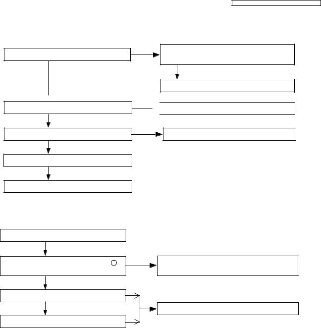
9 Troubleshooting Guide
9.1.Troubleshooting Flowchart
Flow Chart
Power ON Base Unit
OK
Bell
OK
Link
Not Link
OK
Battery Charge
OK
Handset Voice Transmission
OK
Handset Voice Reception
OK
DTMF dial
OK
Caller ID Reception
Cross Reference:
Check Power (P.19)
Bell Reception (P.23)
Check Battery Charge (P.20)
Check Link (P.21)
Check Handset Transmission (P.23)
Check Handset Reception (P.23)
Signal Route (P.12)
Check Caller ID (P.23)
Not Work
Check Power
No Bell
Bell Reception
Not Charge
Check Battery Charge
Check Link
No Voice
Check Handset Transmission
No Voice
Check Handset Reception
No Signal
Signal Route
No Signal
Check Caller ID
18
KX-TG1611RU/KX-TG1612RU/KX-TGA161RU
9.1.1.Check Power
9.1.1.1.Base Unit
Is the AC Adaptor inserted into AC outlet? (Check AC Adaptor’s specification.)
NO
Is input of IC2 (pin3) about 5.5V?
YES
 NO Is the output voltage of IC2 (pin2) about 2.65V?
YES
NO
Is C48(RESETQ) High?
YES
Check X1, C23.
YES
Check Career PCB
Cross Reference
Power Supply Circuit (P.8)
9.1.1.2.Handset
Check F1 is not opened, C34, C35, C58, C60 is not shorted.
YES
Check AC Adaptor.
 Check Power Supply Circuit.
Check Career PCB.
Is the battery inserted to Battery Holder?
YES
Is the voltage of battery between battery + and battery 2.3V more?
YES
Is the voltage of VDDDCDC2 about 3.3 V?
YES
Is C109 (VDDBAT) voltage about 2.3V more?
Cross Reference
Power Supply Circuit/Reset Circuit (P.11)
NO |
Check the battery and around Battery Holder are |
not shorted.
NO
Check Power Supply Circuit/Reset Circuit.
NO
19

KX-TG1611RU/KX-TG1612RU/KX-TGA161RU
9.1.2.Check Battery Charge
9.1.2.1.Base Unit
Plug in the AC Power source.
Charge Handset on Base Unit.
NO
Is the voltage of two charge contacts about Check Power Supply Circuit of Base Unit.
3.0 V and 0V from GND level?
OK
YES
Check Handset.
Check Charge Contacts at
Base Unit from mechanical point of view.
Cross Reference:
Power Supply Circuit (P.8)
9.1.2.2.Handset
|
Is Check Power OK? |
NO |
Check Check Power (Handset). |
||
|
|
|
|||
|
|
|
|
|
|
|
|
YES |
NO |
|
|
|
|
|
|||
|
|
|
|
||
|
Is R101 (CDT) high at charge state? |
Check Charge Circuit. |
|||
|
|
|
|||
|
|
|
|
|
|
Cross Reference: |
|
|
|
||
Check Power (P.19) |
|
|
|
||
Charge Circuit (P.11) |
|
|
|
||
9.1.2.3.Charger Unit
Plug in the AC Power source.
Charge Handset on Charger Unit.
Is the voltage of two charge contacts about |
NO |
Check Power Supply Circuit of Charger Unit. |
|||
|
|
||||
3.0 V and 0V from GND level? |
|
|
|
|
|
|
|
|
OK |
||
|
|
|
|
|
|
|
|
|
|
|
|
|
YES |
|
|
|
|
|
|
Check Handset. |
|||
|
|
|
|
||
|
|
|
|
|
|
Check Charge Contacts at Charger Unit from mechanical point of view.
Cross Reference:
Power Supply Circuit (P.11)
20
Loading...