


 Loading...
Kenwood DDX-6027, DDX-6027-Y, DDX-7017, DDX-7037, DDX-7047 Service manual
...MONITOR WITH DVD RECEIVER
DDX6027/6027Y
DDX7017/7037
DDX7047/7067
SERVICE MANUAL
© 2005-8 PRINTED IN JAPAN B53-0315-00 (N) 1703
Panel assy
(A64-3581-01): DDX7017, (A64-3582-01): DDX7047 (A64-3583-01): DDX6027/6027Y
(A64-3584-01): DDX7037, (A64-3586-01): DDX7067
EJECT FNC 
AVOUT
SEL
SRC
PWROFF
VOL
LOUD 
|
MODE |
|
S |
|
SCRN |
|
DIM |
WITH MONITOR |
SEEK |
RECEIVER DVD |
|
|
AUTO |
Illustrations is DDX7017
Escutcheon |
Escutcheon |
Mounting hardware assy |
Remote controller |
(B07-3105-02) |
(B07-3046-04) |
(J22-0171-03) |
(A70-2072-05 : RC-DV601) |
Size AAA battery
Not supplied
DDX6027/6027Y only |
|
DDX7017/7037/7047/7067 only |
|
|
|
DC cord |
Antena adaptor |
DC cord |
DC cord |
Screw set |
Lever |
(E30-6477-15) |
(T90-0552-05) |
(E30-6475-15) |
(E30-6478-05) |
(N99-1776-05) |
(D10-4674-04) x2 |
This product uses Lead Free solder.
DDX6027/6027Y/7017
DDX7037/7047/7067
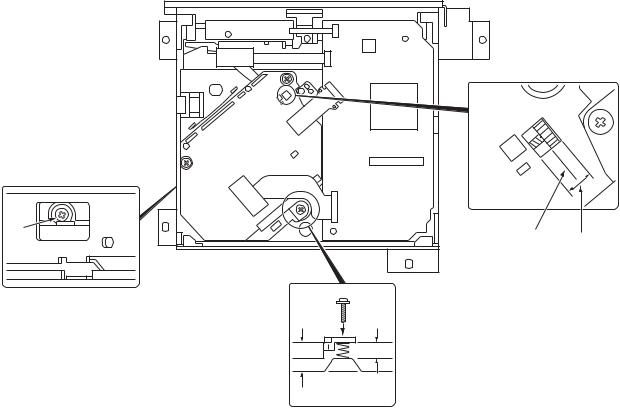
NOTES ON ASSEMBLING THE MECHANISM
1.Fasten Screw A so that the interval (a) will be about 5.2mm and the interval (b) will be about 2.6mm. (The interval (a) can be measured using a pair of vernier calipers or similar tools.)
2.Turn B so that Position (c) will come at about the center of interval (d).
3.Then, play the test disc and fine tune A or B so that the jitter value would be minimized.
B |
|
c |
d |
|
|
||
|
|
|
|
5.2mm |
A |
2.6mm |
|
|
|
|
|
|
|
b |
|
a |
|
|
|
2
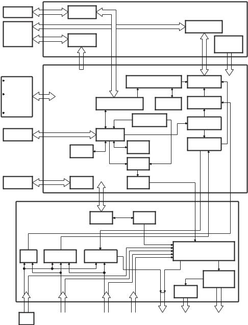
● Complete view
TOUCH
LCD
(X16- )
SMALL
DISPLAY
REMOTE
CONTROL
RECEIVER
KEY
DVD
MECHA
SLIDE
MECHA
(X34- )
RGB
SW
TV
I/F
DDX6027/6027Y/7017
DDX7037/7047/7067
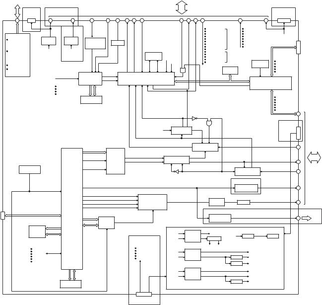
BLOCK DIAGRAM
(X35- )
TOUCH
CONTROL
|
|
|
TIMING |
|
|
|
CONTROLLER |
INVERTER |
|
|
REMOTE |
CIRCUIT |
|
|
|
|
|
CONTROL |
|
|
|
|
RECEIVER |
(X14- ) |
|
|
|
|
OSD |
|
CHROMA |
|
|
GAMMA IC |
|
|
|
|
|
|
SYSCON |
SDRAM |
RGB SW |
|
CLOCK |
|
VIDEO |
|
OSCILLATOR |
||
|
ENCODER |
||
|
|
|
|
|
MPEG |
|
|
|
|
|
COMPOSITE |
SDRAM |
FLASH |
|
SW |
|
|
|
|
|
CPLD |
|
|
MOTOR |
AUDIO |
|
|
DRIVER |
DAC |
|
|
BOX |
AM/FM |
u-COM |
TUNER |
AUDIO
INPUT SELECTOR
COMPOSITE |
COMPOSITE |
SW |
SW |
AUDIO
OUTPUT
SELECTOR
POWER
AMP
NAVI |
|
AV-IN |
|
LX-BUS |
|
AV OUT |
|
SP |
|
PRE |
I/F |
|
I/F |
|
I/F |
|
I/F |
|
OUT |
|
OUT |
3
DDX6027/6027Y/7017
DDX7037/7047/7067
|
|
|
|
|
|
|
|
BLOCK DIAGRAM |
|
|
|
|
|
|||||||||
● X14-957/958 |
|
|
|
|
|
|
|
|
|
|
|
|
|
|
|
|
|
|
|
|
|
|
|
|
|
|
|
|
|
|
|
|
|
|
|
|
to X35 |
|
|
|
|
|
|
||
to X16 |
|
|
|
|
|
|
|
|
|
|
|
|
|
|
|
|
|
|
|
|
|
|
|
2DIN ONLY |
1DIN ONLY |
|
|
|
|
|
|
|
|
|
|
|
|
|
|
|
|
|
|
|
2DIN ONLY |
(X14-957 |
to MECHA |
|
|
|
|
|
|
|
|
|
|
|
|
|
|
|
|
|
|
|
|
to SUB PANEL |
/958) |
|
|
|
|
|
|
|
|
|
|
|
|
|
|
|
|
|
|
|
|
||
|
|
|
|
|
|
|
|
|
|
|
|
|
|
|
|
|
|
|
|
|
|
|
|
|
|
|
|
|
PLLCLK |
|
VSY |
HSY |
RGB |
VCOM |
POLS |
|
BLK |
T/CHD |
T/C V |
to SYSCOM |
|
|
from SYSCOM |
|
|
|
|
RL M+ |
|
EX M+ |
|
|
SW D |
|
|
Y0 |
|
|||||||||||
|
|
|
|
|
|
|
|
|
|
|
|
|
|
|
XDATA |
|
|
X0 |
|
|||
|
|
RL M- |
|
EX M- |
|
|
|
|
|
|
|
|
|
|
|
|
YDATA |
|
|
X1 |
|
|
from SYSCOM |
IC203 |
IC202 |
|
|
|
|
|
|
|
|
|
|
|
|
|
|
AUTO DIMMER |
1DIN |
MODE1,2,3 |
LED R |
||
LCD CONTROL |
MOTOR |
MOTOR |
|
1.5 |
|
|
|
|
|
|
|
|
|
|
|
PH DET |
|
HPOSI1,2,3,4 |
LED G |
|||
|
|
|
|
|
|
|
|
|
|
|
|
|
ONLY |
|||||||||
|
|
|
|
|
|
|
|
|
|
|
|
R SENS |
|
NTSC PAL |
|
|||||||
LCD CS |
|
DRIVER |
DRIVER |
|
FREQUENCY |
MM |
|
|
|
|
|
|
|
|
|
|
|
|||||
LCD DATA |
|
|
|
|
|
|
|
|
|
|
SW A,B,C |
|
|
PWM |
|
|||||||
LCD CLK |
|
|
|
|
|
DIVIDING |
|
|
|
|
|
|
|
|
|
|
KEY1 |
|
|
MIRROR |
|
|
KEY CONTROL |
TMOTOR M |
SMOTOR M |
|
|
|
|
|
|
|
IC301 |
|
|
|
|
|
OPEN/CLOSE |
|
|
|
|||
|
9.6MHz |
|
|
|
|
|
|
4.43MHz |
|
|
|
KEY3 |
|
ONLY |
IC206 |
to ROM WRITER |
||||||
SRC |
|
TMOTOR P |
1DIN ONLY |
|
|
|
|
|
|
|
|
|
|
|
REMO |
|
||||||
KEY2 |
|
SMOTOR P |
|
|
|
|
|
|
|
1H DELAY |
|
|
|
|
KEY4 |
|
2DIN |
|
|
|||
RESET |
|
|
|
|
|
|
|
|
|
|
|
|
|
|
|
SRC |
|
|
|
|||
|
|
|
|
|
|
|
|
|
|
|
|
|
|
|
|
|
|
|
||||
EJECT |
|
|
|
|
|
DCLK |
|
|
|
|
|
-RY |
Y-B |
3.58MHz |
|
|
|
EJECT |
|
|
RESET IC |
RESET |
REMO |
|
|
|
|
|
|
|
|
|
|
|
|
|
|
|
IC200 |
M CLK |
|||||
LED R,G,B |
|
|
|
|
|
|
|
|
|
|
|
|
|
|
|
|
|
|
|
|
|
M DATA |
|
|
|
IC400 |
|
|
IC303 |
|
|
|
|
|
|
|
|
E2PROM |
|
S DATA |
|||||
|
|
|
|
|
|
|
|
|
|
|
|
|
|
|
FROM VPP |
|||||||
1DIN ONLY |
|
|
|
|
|
|
|
|
|
|
|
|
|
|
|
|
|
|
|
|
|
|
|
|
|
|
|
|
|
OSD RGB |
|
|
|
|
|
|
|
|
SCL |
|
|
IC204 |
|
||
|
|
|
|
|
|
OSD IC |
|
OSD BLK |
|
|
CHROMA GAMMA IC |
|
|
|
|
|
|
|
|
|||
|
|
|
|
|
|
|
|
|
|
|
|
|
SDA |
|
|
|
|
|||||
|
|
from SYSCOM |
|
|
|
|
|
|
|
|
|
|
|
|
VMUTE |
|
|
SYSCOM |
||||
|
|
OSD DATA |
|
|
|
|
|
|
|
|
|
|
|
|
|
|
|
|||||
|
|
|
|
|
|
|
|
|
|
|
|
|
|
|
|
|
|
|
|
|
||
|
|
OSD CLK |
OSD A(17:0) |
OSD D(11:0) |
|
|
|
|
|
|
|
|
|
|
|
|
|
|
||||
|
|
OSD CS |
|
|
|
|
|
|
|
|
|
|
|
|
|
to BOX MCU |
||||||
|
|
|
IC401 |
|
|
|
|
|
|
|
|
|
|
|
|
|
|
|
||||
|
|
OSD RST |
|
|
|
|
|
|
|
|
|
|
|
|
|
|
|
|
||||
|
|
|
|
|
|
|
|
|
|
|
|
|
|
|
|
|
|
M CLK |
||||
|
|
|
|
|
|
FROM |
|
|
|
|
|
|
|
|
|
|
|
|
|
|
|
|
|
|
|
|
|
|
|
|
|
|
|
|
|
|
|
|
|
|
|
|
|
M REQ |
|
|
|
|
|
|
|
|
|
|
|
|
|
|
|
|
|
|
|
|
|
|
|
S REQ |
|
|
|
|
|
|
|
|
|
|
|
|
|
|
|
|
|
|
|
|
|
|
M DATA |
|
|
|
|
|
|
|
|
|
|
|
|
|
|
|
|
|
|
|
|
|
|
S DATA |
|
|
|
|
|
|
|
|
|
|
|
|
|
|
|
|
|
|
|
|
|
|
SYS ON |
|
|
|
|
|
|
|
|
|
|
|
|
|
|
IC362 |
HD |
VD |
|
|
|
|
|
2DIN ONLY |
|
|
|
|
|
|
|
|
|
|
|
|
|
|
|
|
|
|
|
|
|
|
|
|
|
|
|
|
|
|
|
|
|
|
|
NTSC PAL |
SYNC SEPA |
CP |
|
|
|
|
|
|||
|
|
|
|
|
|
|
|
|
|
|
|
|
|
|
|
|
|
|||||
|
|
|
|
|
|
|
|
|
|
|
|
COMPOSITE |
|
|
|
|
|
|
|
|
|
+B |
|
|
|
|
|
|
|
|
|
|
|
|
|
|
|
|
|
|
|
|
|
ACC |
|
|
|
|
|
|
|
|
|
|
|
|
|
|
|
|
|
|
IC304 |
|
|
|
|
GND |
|
|
|
|
|
|
|
|
|
|
|
|
|
|
|
|
|
|
|
|
|
|
|
|
|
|
IC601 |
|
|
|
|
IC652 |
|
|
RGB |
|
|
|
|
|
RGB SW |
|
|
|
TV/NAVI RG |
|
|
|
|
|
|
CCIR601(7:0) |
|
|
|
|
|
|
|
|
|
|
|
|
|||||
|
|
|
|
|
|
|
|
|
|
|
|
|
|
|
|
|
|
|
|
|
||
|
|
|
MPEG |
|
|
|
|
|
|
|
|
DVDRGB |
|
IC650 |
|
|
DVDRGB |
|
|
|
|
|
|
|
|
DECODER |
|
VCLOCK |
VIDEO |
|
|
|
LPF+6dB AMP |
|
|
|
|
|
|
||||||
|
|
|
|
|
|
DVDCOMP V |
|
|
|
|
|
|
|
DVDCOMP V |
||||||||
|
|
|
|
|
|
|
|
ENCODER |
|
|
|
+DRIVER+MUTE |
|
|
|
|
|
|||||
|
|
|
|
|
|
|
|
|
|
|
|
|
|
|
|
|
|
|||||
27MHz |
|
|
|
|
HSYNC |
|
|
|
|
|
|
|
|
|
|
|
|
|
IC654 |
|
||
|
|
|
|
VSYNC |
|
|
|
|
|
|
|
MUTE |
|
|
RGB SW |
|
|
|
|
VIDEO |
||
OSCILLATOR |
|
|
|
|
|
|
|
|
|
|
|
|
|
|
|
|
|
|
VIDEO SW |
|||
|
|
|
|
|
|
|
|
|
|
|
|
|
|
|
|
|
|
|
|
|||
|
27MHz |
|
|
|
|
|
|
|
|
|
|
|
|
|
|
|
|
|
|
2DIN ONLY |
|
|
|
|
|
|
|
|
|
|
SPDIF |
|
|
|
|
|
|
|
|
|
|
|
BUFFER |
|
|
|
|
|
|
|
|
|
|
|
DATA1 |
|
|
IC703 |
|
|
|
|
|
|
|
|
|
|
|
|
|
|
|
|
|
|
|
|
|
|
|
|
|
|
|
IC701 |
|
|
|
|
|
|
|
|
|
|
|
|
|
|
BCLK |
|
|
|
|
|
|
|
|
|
|
|
DOWNMIX |
|
|
|
|
|
|
|
|
|
|
|
|
2ch AUDIO DAC |
|
|
|
|
|
|
|
||||
|
|
|
|
|
|
|
|
|
LRCLK |
|
|
|
|
|
LPF |
|
|
MUTE |
AUDIO |
|||
|
|
|
|
|
|
|
|
|
|
|
|
|
|
|
|
|
|
|
|
|||
|
|
|
|
|
|
|
|
|
MCLK |
|
|
|
|
|
|
|
|
|
|
|
|
|
to DVD |
ATAPI I/F |
|
LA17 |
|
ADACML |
|
1DIN ONLY |
|
|
|
|
IC770 |
|
|
|
|
|
||||
|
|
ADACMC |
|
|
|
|
|
|||
MECHA |
|
|
LA(1:0) |
|
ADACMD |
|
OPT DRIVER |
|
|
|
|
|
|
LD(3:0) |
CPLD |
ADACRST |
|
|
|
|
|
|
IC560 |
|
|
|
|
|
|
|
||
|
A(11:1) |
|
|
|
|
|
|
|
|
|
|
|
|
|
|
|
|
|
|
|
|
|
SDRAM |
D(15:0) |
|
27MHz |
1DIN ONLY |
PON |
TRANCE |
BU3.3V |
|
|
|
|
|
|
|
|
+14.4V |
+8.5V |
MPU |
||
|
|
|
|
|
|
DC/DC |
|
+14.4V |
REG |
|
|
SYSCOM |
|
|
|
to SYSCOM |
|
+7V |
-7V |
|
|
|
BE RST |
|
|
|
ACC DET |
|
|
|
||
|
|
|
|
|
|
|
|
|
||
|
BE CLK |
|
|
|
REV DET |
+14.4V |
|
|
SW5V |
|
|
BE MREQ |
|
|
|
PRK DET |
DC/DC |
MECHA 7V |
|
|
|
|
BE SREQ |
|
|
|
ILLUMI |
|
|
|||
|
|
|
|
PON |
|
REG |
MECHA5V |
|
||
|
BE MDATA |
|
|
|
REMO |
|
|
|||
|
BE SDATA |
|
|
|
|
|
|
REG |
V5V |
|
|
|
|
|
|
|
|
|
|
||
|
|
|
|
|
+B |
+14.4V |
|
|
+7.5V |
|
|
|
|
|
|
ACC |
|
|
|
||
|
|
A(21:0) |
D(7:0) |
|
GCD |
DC/DC |
|
|
SW3.3V |
|
|
|
IC520 |
|
|
|
PON |
|
|
|
|
|
|
|
|
|
|
|
REG |
|
|
|
|
|
FLASH |
|
|
|
|
SW2V |
|
||
|
|
|
|
POWER SUPPLY |
|
|
|
|
||
|
|
|
|
|
|
|
|
|
|
|
POWER SUPPLY
CONNECTOR
to X34
OPT
OUT
4

LX I/F
LX CON LX CLK LX DATA M LX DATA S LX REQ M LX REQ S LX MUTE LX RST
AUD Lch
AUD Rch
A GND
NV I/F
RX
TX
REMO
SYNC
R
G
B
AUD Lch
AUD Rch
A GND
to TV TUN
TV CON TV CLK TV DATA M TV DATA S TV REQ M TV REQ S
M RST
COMP V
R
G
B
TV Lch
TV Rch
A GND
to X14
M CON M CLK M DATA M M DATA S M REQ M M REQ S
REMO
M RST
COMP V
R
G
B
DVD COMP
DVD Lch
DVD Rch
A GND
REVERSE ILLUMI ACC PARK W-REMO
BU
GND
8 MCU
|
IC500 |
3 |
ISO AMP |
|
|
|
2 |
|
MCU |
FST |
|
|
|
|
FM AM F/E |
|
|
|
|
A OUT |
|
IC251 |
|
|
|
|
|
||
|
|
RDS |
|
|
MPX for RDS |
BUFF |
DECODER |
|
|
|
|
|||
PON AM |
MCU |
QUAL |
3 |
|
RDDA |
||||
|
|
MCU |
||
|
|
RDCL |
|
|
S-METER |
|
|
|
|
IF COUNT |
4 |
|
|
|
SCL |
|
|
||
SDA |
MCU |
|
|
|
QUALITY |
|
|
|
|
RDS MUTE |
|
|
|
|
2 |
|
|
|
|
|
|
IC413 |
||
IC151 |
|
INPUT SEL |
|
TUNE |
MAIN |
AUX |
|
CDCH |
SUB |
CD |
|
MD |
AUX |
LEVEL ADJUST
MUTE
LEVEL ADJUST
MUTE
LEVEL ADJUST
MUTE
MCU 4
SCL
SDA
S-MUTE
DCERR
LEVEL ADJUST
TONE
EQ
VOL IN
|
3 |
|
|
|
3 |
|
|
|
|
IC400-402 |
|
|
|
R SW |
|
|
|
G SW |
|
|
6 |
B SW |
|
|
|
|
|
|
MCU |
|
|
|
|
2 |
|
|
|
MCU |
|
3 |
|
|
|
|
IC405 |
IC416 |
|
|
|
|
|
3 |
ISO AMP |
VIDEO |
|
|
|
||
|
SEL |
2 |
|
|
|
||
|
|
|
MCU |
|
|
IC406 |
|
|
|
VIDEO |
|
|
|
SEL |
2 |
|
6 |
|
MCU |
|
MCU |
|
|
|
|
|
|
|
|
IC415 |
|
|
|
VIDEO |
|
|
|
SEL |
1 |
|
|
MCU |
MCU |
|
|
|
|
3 |
|
|
|
3 |
|
|
|
7 |
|
|
|
AUDIO |
|
|
SEL |
2 |
|
|
MCU |
|
IC414 |
|
|
AUDIO |
2 |
|
SEL |
||
|
||
|
MCU |
IC408 |
|
VIDEO SEL |
|
6dB AMP |
|
75 |
DRIVER |
IC407 |
|
VIDEO SEL |
|
6dB AMP |
|
75 |
DRIVER |
2 MCU
2 MCU
IC303
MCU
IC404
VIDEO SEL
2
MCU
IC403
SYNC SEP
OUTPUT SEL |
|
|
|
|
||
ACIN0 |
|
|
|
|
PAOUT0 |
|
(FRONT) |
FRONT |
HPF |
MUTE |
VOL |
(FRONT) |
|
ACIN1 |
(FRONT) |
(FRONT) |
(FRONT) |
PAOUT1 |
||
|
||||||
(REAR) |
|
|
|
|
(REAR) |
|
ACIN2L |
|
|
|
|
LDOUT0 |
|
(CENTER) |
REAR |
HPF |
MUTE |
VOL |
(FRONT) |
|
ACIN2R |
(REAR) |
(REAR) |
(REAR) |
LDOUT1 |
||
|
||||||
(SUB-W) |
|
|
|
|
(REAR) |
|
2ZONE |
CENTER |
|
MUTE |
VOL |
LDOUT2L |
|
MAIN |
LPF |
(CEN/NF) |
||||
/NF L |
(CEN |
(CEN |
||||
2ZONE |
(NF) |
LDOUT2R |
||||
SUB-W |
SUB) |
SUB) |
||||
SUB |
|
|
|
|
(SUB/NF) |
|
POWER SUPPLY |
|
|
|
|
||
BU |
SW |
SW14V |
BU |
REG |
A8V |
|
PON |
SW14V |
|||||
|
|
|
|
|||
|
|
|
BU |
REG |
V5V |
|
|
|
|
SW14V |
|||
|
|
|
|
|
||
|
|
|
|
REG |
BU5V PON |
|
MCU |
|
|
BU |
SW |
||
|
IC100 |
|
|
POWER |
|
|
AMP |
FL+ - |
|
|
FR+ - |
|
|
RL+ - |
|
|
RR+ - |
4 |
STBY |
|
MUTE |
|
|
MCU |
BEEP |
|
|
SVR |
|
IC2VI |
|
|
|
|
8 |
|
|
IC200-202 |
MUTE |
|
AMP |
MCU
MUTE
MCU
IC204
ISO AMP
IC203
ISO AMP
SW5V
384/385-X34 ●
DC
BU
GND
SMALL
P.CON
ATT.CON
LINE MUTE
EXT.CONT
SP OUT
PRE OUT
FRONT L
FRONT R
REAR L
REAR R
NF L
NF R
AV OUT
V
L
R
AV IN1
V
L
R
AV IN2
V
L
R
R-CAM
V
DC 8PIN
REVERSE
ILLUMI
ACC
PARK
W-REMO
BU
GND
5
DIAGRAM BLOCK
DDX7037/7047/7067 |
DDX6027/6027Y/7017 |

DDX6027/6027Y/7017
DDX7037/7047/7067
BLOCK DIAGRAM
● X35-458/459 |
|
|
|
|
|
|
|
|
|
||
|
|
|
|
|
VR/VG/VB |
|
|
|
|
|
|
|
2DIN TYPE |
1DIN TYPE |
|
|
PON+5.0V |
|
|
|
|
NC |
|
1 |
PON+5.0V |
PON+5.0V |
|
|
|
|
PON-12.0V |
|
|||
|
|
|
|
|
VGL-12.0V |
|
|||||
2 |
PON+5.0V |
PON+5.0V |
|
|
PON+3.3V |
|
|
|
|
|
|
|
|
|
|
|
|
NC |
|
||||
3 |
NC |
NC |
|
|
VGND |
|
|
VGND |
|
2DIN ONLY |
|
4 |
VGND |
VGND |
|
|
|
|
|
VSS |
|||
|
|
IC101 |
|
|
|
|
|
||||
5 |
VGND |
VGND |
|
|
|
|
|
|
STV1 |
|
|
|
|
|
PON-12.0V |
|
|
|
STV1 |
6.5 INCH |
|||
6 |
SW+18.5V |
SW+18.5V |
OPEN |
|
|
|
|
|
UPSD |
||
7 |
DGND |
DGND |
|
|
DC-DC |
PON+18.5V |
|
|
|
U/D(UPSD) |
LCD |
|
|
|
|
|
CPV |
||||||
8 |
EJECT |
OPEN |
|
|
IC |
PON+12.5V |
|
|
|
CPV |
|
CLOSE |
|
|
|
|
|
|
|
NGOE3 |
|
||
|
|
|
|
|
|
|
|
|
OE3(NGOE3) |
|
|
9 |
KEY3 |
NC |
|
|
|
|
|
|
|
NGOE2 |
|
|
|
|
|
|
|
|
OE2(NGOE2) |
|
|||
10 |
KET4 |
T/C VD |
|
|
|
|
|
|
|
NGOE1 |
1DIN ONLY |
|
|
|
|
|
|
|
OE1(NGOE1) |
||||
11 |
LED GND |
LED GND |
|
|
|
IC203 |
|
|
|
STV2 |
|
12 |
SI |
BRINK |
|
|
VCOM |
|
PON+3.3V |
STV2 |
7 INCH |
||
|
|
|
|
VDD1+3.3V |
|||||||
13 |
NC |
NC |
|
|
COM AMP |
||||||
|
|
|
PON+5.0V |
LCD |
|||||||
14 |
PLL CLK |
PLL CLK |
|
|
VGND |
|
|
VDD2+5.0V |
|||
|
|
|
|
|
|
|
|||||
15 |
LED G |
LED G |
|
|
|
|
|
|
NC |
|
|
|
|
|
|
|
PON+18.5V |
|
|||||
16 |
LED R |
LED R |
|
|
|
IC301 |
|
VGH+18.5V |
|
||
17 |
NC |
NC |
|
|
|
|
|
|
|
||
|
|
PON+3.3V |
|
|
|
NC |
|
||||
18 |
PON+3.3V |
PON+3.3V |
|
|
|
V.COM |
|
|
|||
|
|
|
|
|
|
VCOM |
0.5mm |
||||
19 |
NC |
NC |
|
|
|
|
|
|
|
||
20 |
VGND |
VGND |
|
IC302 |
|
|
|
|
|
VSS |
30PIN |
21 |
VB |
VB |
|
|
|
|
|
|
|
VSS |
|
22 |
VG |
VG |
|
|
|
|
|
|
|
CPH1 |
|
23 |
VR |
VR |
|
|
|
|
|
UPSD/CPV/ HDIR/CX/ |
CPH(CPH1) |
|
|
|
|
|
|
|
VSS |
|
|||||
24 |
VGND |
VGND |
|
|
|
|
|
STV1/STV2/STH1/STH2/ |
|
||
|
|
|
|
|
CX |
|
|||||
25 |
T/C HD |
T/C HD |
|
|
|
TIMMING |
|
NGOE1/NGOE2/ |
|
CX |
|
26 |
V GND |
V GND |
|
|
|
|
NGOE3/CPH1 |
|
HDIR |
|
|
|
|
|
CONTROLLER |
|
|
L/R(HDIR) |
|
||||
27 |
NTSC/PAL |
NTSC/PAL |
|
|
|
|
|
STH1 |
|
||
|
|
|
|
|
|
|
STH1 |
|
|||
28 |
PLL ON |
PLL ON |
|
|
|
|
|
|
|
VSS |
|
29 |
POLS |
POLS |
POLS/HSY/VSY/BLK |
|
|
|
|
VB |
|
||
30 |
MIRROR |
MIRROR |
|
|
|
|
VB |
|
|||
|
|
|
|
|
|
|
VG |
|
|||
31 |
VSY |
VSY |
|
|
|
|
|
|
|
VG |
|
32 |
HSY |
HSY |
|
|
|
|
|
|
|
VR |
|
|
|
|
|
|
|
|
VR |
|
|||
33 |
BLK |
BLK |
|
|
|
|
|
|
|
STH2 |
|
MODE1/2/3/HPOS1/2/3/4 |
|
|
|
STH2 |
|
||||||
34 |
MODE3 |
MODE3 |
NTSC/PAL,MIRROR |
|
|
|
|
NC |
|
||
35 |
MODE2 |
MODE2 |
|
|
|
|
|
||||
|
|
|
|
|
|
|
|
|
|||
36 |
MODE1 |
MODE1 |
|
|
|
PDOS/OSCI |
|
|
|
|
|
37 |
HPOS4 |
HPOS4 |
|
|
|
|
|
|
|
||
|
|
|
|
|
|
|
|
|
|||
38 |
HPOS3 |
HPOS3 |
|
|
|
IC303 |
PLL & LPF |
|
|
CFL |
|
39 |
HPOS2 |
HPOS2 |
|
|
|
TOUCH PANEL |
|||||
|
|
|
|
|
|
|
|||||
40 |
HPOS1 |
HPOS1 |
|
|
|
|
|
|
|
||
|
|
|
|
|
|
|
|
|
|||
41 |
NC |
NC |
|
|
|
|
|
|
|
|
|
42 |
VCOM |
VCOM |
|
|
|
|
|
|
|
X0/X1/ |
|
43 |
NC |
NC |
|
|
|
|
|
|
|
Y0/Y1 |
|
44 |
PON+3.3V |
PON+3.3V |
|
|
|
|
|
|
TOUCH PANEL |
BACK LIGHT |
|
45 |
BU+3.3V |
AUTO DIM |
|
|
|
|
|
|
|||
|
|
|
|
|
|
SWITCH CIRCUIT |
INVERTER |
||||
46 |
NC |
KEY1 |
|
|
|
|
|
|
|||
|
|
|
|
|
|
|
|
|
|||
47 |
XDATA |
XDATA |
|
|
|
|
|
|
|
|
|
48 |
YDATA |
YDATA |
|
|
1 |
SW-D |
|
1DIN ONLY |
PON+5.0V |
|
|
49 |
X0 |
X0 |
|
|
|
|
XDATA/YDATA |
|
|||
|
|
2 |
SW-C |
|
|
|
|||||
50 |
X1 |
X1 |
|
|
|
|
|
|
|
||
|
|
3 |
SW-B |
|
|
X0/X1/Y0 |
|
|
|||
51 |
Y0 |
Y0 |
|
|
|
|
|
|
|||
52 |
SRC |
NC |
|
|
4 |
SW-A |
|
|
|
|
|
|
|
5 |
NC |
|
|
|
|
|
|||
53 |
PWM |
PWM |
|
|
|
|
|
1DIN ONLY |
|||
|
|
6 |
EX M+ |
|
|
|
|||||
54 |
ENABLE |
ENABLE |
|
|
|
|
|
||||
|
|
7 |
EX M+ |
|
|
|
|
|
|||
55 |
T/C VD |
SW-D |
|
|
|
|
|
IC401 |
|
||
|
|
8 |
EX M- |
7 INCH |
|
|
|
||||
56 |
NC |
NC |
|
|
|
AUTO DIM/ |
|
|
|||
|
|
9 |
EX M- |
|
AUTO DIMMER |
||||||
57 |
BL GND |
BL GND |
|
|
INDASH MECHA |
||||||
|
|
10 |
RI M+ |
KEY1 |
|
|
|||||
58 |
BL GND |
BL GND |
|
|
|
|
|
|
|
||
|
|
11 |
RI M+ |
|
|
|
|
|
|||
59 |
NC |
NC |
|
|
|
|
|
SW PCB B/3 |
|
||
|
|
12 |
RI M- |
|
|
|
|
||||
60 |
BL +8.5V |
BL +8.5V |
|
|
|
|
|
|
|
||
|
|
13 |
RI M- |
|
|
|
|
|
|||
61 |
BL +8.5V |
BL +8.5V |
|
|
|
|
|
|
|
||
|
|
14 |
NC |
|
|
|
|
|
|||
62 |
NC |
NC |
|
|
|
|
|
|
|
||
|
|
15 |
RSENS |
|
|
|
|
|
|||
63 |
NC |
DGND |
|
|
|
|
|
|
|
||
|
|
16 |
REF+5.0V |
|
|
PWM/ENABLE |
|
||||
64 |
ESD GND |
PH DET |
|
|
|
|
|
||||
|
|
17 |
SW+5.0V |
|
|
|
|
|
|||
65 |
ESD GND |
SW+5.0V |
|
|
|
|
|
|
|
||
|
|
18 |
PH DET |
|
|
D.GND |
|
|
|||
66 |
BL DET |
BL DET |
OPEN |
|
|
|
|
||||
19 |
NC |
|
|
|
|
|
|||||
67 |
RESET |
RSENS |
|
|
|
|
|
|
|
||
|
|
|
|
|
|
LED GND |
|
|
|||
68 |
REMO |
NC |
|
|
|
|
|
|
|
|
|
|
|
|
|
|
|
BL8.5V |
|
|
|||
69 |
|
RI M- |
|
|
|
|
|
|
|
|
|
70 |
|
RI M- |
TR SW |
|
|
|
2DIN ONLY |
BL GND |
|
|
|
71 |
|
RI M+ |
|
|
|
|
|
|
|
||
72 |
|
RI M+ |
BU3.3V |
|
SI3.3V |
|
D GND |
PON+5.0V |
|
|
1DIN ONLY |
73 |
|
EX M- |
|
|
|
|
|
|
|||
74 |
|
EX M- |
SI |
|
|
|
LED+8.5V(B) |
|
|||
75 |
|
EX M+ |
|
|
|
LED+8.5V(R)/LED+8.5V(G) |
|
||||
|
|
|
LED_G,LED R,SI3.3V |
|
|
|
|||||
76 |
|
EX M+ |
|
|
RESET,SRC,EJECT,KEY3 |
SW PCB |
LED GND |
|
|
||
77 |
|
NC |
|
|
|
SW PCB |
|||||
|
|
|
|
|
DGND |
|
|||||
78 |
|
SW-A |
|
|
KEY4,REMO.ESD GND |
|
|
|
C/3 |
||
|
|
|
|
|
OPEN CLOSE/VOL+/VOL- |
||||||
79 |
|
SW-B |
|
|
|
|
|
|
|
||
80 |
|
SW-C |
|
|
|
|
|
|
BRINK |
|
|
6
|
|
DISC |
|
|
|
|
|
|
|
|
DVD LD/CD LC |
|
|
A5V |
|
|
VC (2.2V) |
|
SPINDLE |
|
|
||
|
|
|
PD/VR DVD/VR CD |
||
|
MOTOR |
OPTICAL |
|||
|
I/V OUT (DVD/CD) |
||||
|
|
|
|||
|
|
|
PICK UP |
||
|
|
|
MODE SW/GAIN SW |
||
SWLIM |
HALLBIAS U,V,W,COIL |
HALLSENSOR |
|
|
|
|
|
CN1 CONNECTOR (24P,0.5PITCH) |
|||
|
|
|
|
|
FO+-,TR+- |
|
|
2 PHASE |
|
|
|
|
|
STEPPING MOTOR |
|
||
|
|
CN3 |
4 |
CN2 |
|
|
|
CONNECTOR |
|
CONNECTOR |
|
|
|
(18P,0.5PITCH) |
|
(10P,0.5PITCH) |
|
|
|
|
|
P5V |
|
|
|
IC2 |
|
|
|
|
|
7 |
PWM*2 |
|
|
|
|
|
|
PWM*2 |
|
33PHASE PWM
VHALF
P5V |
VREF,EC |
MOTOR &
ACTUATER
DRIVER
LO/EJ
DC MOTOR
M |
|
FG |
|
|
|
||
CN6 |
|
|
|
CONNECTOR |
|
||
(2P,PIN ASSY) |
|
||
CONNECTOR |
C |
||
D |
|||
(4P,0.5PITCH) |
|||
E |
|||
CN1 |
CN5 |
||
|
|||
A |
|
|
|
B |
|
|
|
FFC |
|
|
|
|
|
D3.3V |
|
A3.3V |
IC5 |
|
|
|
|
|
16.897849MHz |
|
|
RESET IC |
|
|
THERMISTER |
APC TR |
|
D5V A3.3V D3.3V 1.5V |
IC4
|
Q7,Q8 |
A5V A3.3V |
|
|
|
|
|
|
IC1 |
|
|
|
|
|
2 |
|
|
|
3 |
|
FRONT END |
7 |
|
|
PROCESSOR |
||
|
|
||
8 |
A,B,C, |
|
|
|
D,E,F,RF (P,N) |
VHALF |
|
|
|
SEN |
|
|
|
|
|
|
VR |
SCK,STDI |
|
|
|
|
|
|
|
|
3 |
Q1,Q2 |
|
|
|
TEMP DET (AD) |
|
|
|
IOP- (AD) |
|
|
|
ARF,NARF |
|
|
|
FBAL |
|
|
|
JLINE,TSTSG |
|
|
|
FE,AS,REFNV,RFDIFO |
|||
OFTR,BDO,VREF2 |
|
|
|
VHALF (16.5V) |
SPDRV,FODRV,TRDRV |
PWM8,DRV.MUTE,LO.MTE,B |
A,STEPMS,STEPB |
SWGAIN |
|||
TRCRS |
|
|
|
TE |
|
|
|
SEN |
|
|
|
SCK,STDI |
|
|
|
DVDON/CDON |
|
|
|
NRST
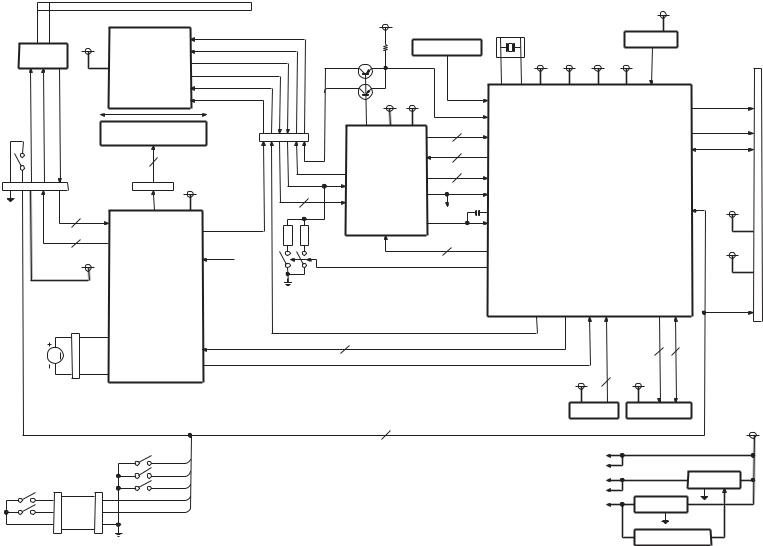
OPTICAL DISC CONTROLLER
|
|
SW A,B,C,D,E |
|
|
LIM-SW |
FG,EXCNT1 |
SDA,SCL |
FADR0-FADR17, NCE,NWE,NOE FDT0-FDT7 |
CN4 CONNECTOR (50P,0.5PITCH)
S/P DIF
CD-DA
AUDIO OUT
ATAPI IF
D5V
P5V
DISC DET
mechanism) (DVD 107-X37 ●
9 |
|
|
21 |
8 |
|
|
|
||
|
D3.3V |
2 |
D3.3V |
|
IC11 |
EEPROM |
FLASH ROM |
||
|
||||
6 |
|
|
IC3 |
D5V |
|
|
|
|
|
|
A5V |
|
IC10 |
|
|
D5V |
|
||
|
A3.3V |
IC9 |
3.3V REG. |
|
|
D3.3V |
|
||
|
1.5V |
1.5V REG. |
||
|
|
|
IC8 |
|
|
|
|
VOLTAGE DET |
|
7
DIAGRAM BLOCK
DDX7037/7047/7067 |
DDX6027/6027Y/7017 |
DDX6027/6027Y/7017
DDX7037/7047/7067
COMPONENTS DESCRIPTION
● VIDEO CONTROL UNIT (X14-957/958x-xx)
Ref. No. |
Application / Function |
Operation / Condition / Compatibility |
|
|
|
|
|
IC100 |
DC-DC power supply IC |
SW5V/MECHA7V control |
|
|
|
|
|
IC101 |
DC-DC power supply IC |
SW3.3V/MECHA7.5V control |
|
|
|
|
|
IC102 |
DC-DC power supply IC |
BL8.5V, ±7V control |
|
|
|
|
|
IC103 |
Regulator IC |
Backup 5V generation |
|
|
|
|
|
IC104 |
Regulator IC |
Backup 3.3V generation |
|
|
|
|
|
IC108 |
Regulator IC |
IC601 2V generation |
|
|
|
|
|
IC200 |
E2PROM |
Memory for µ-com |
|
|
|
|
|
IC203 |
Motor driver IC |
Tilt mechanism tilt control |
|
|
|
|
|
IC204 |
System microcomputer |
For main unit control |
|
|
|
|
|
IC205 |
Logic IC (AND) |
AND for remote controller + wired remote-controlled |
|
|
|
|
|
IC206 |
Resetting IC |
For resetting µ-com |
|
|
|
|
|
IC207 |
Logic IC (AND 4) |
For 3.3V → 5V conversion |
|
|
|
|
|
IC301 |
Color differential signal 1H-DELAY |
For delaying color differential signal for 1H at the time of PAL |
|
|
|
|
|
IC303 |
Color liquid crystal panel driving signal |
RGB signal generation for liquid crystal |
|
processing IC |
|||
|
|
||
|
|
|
|
IC304 |
RGB switch |
For switching DVD signal and RGB signal coming from X34 |
|
|
|
|
|
IC306 |
Logic IC (Inverter) |
For reversing blank signal coming from X35 |
|
|
|
|
|
IC361 |
Logic IC (NAND) |
HD signal reversal buffer |
|
|
|
|
|
IC362 |
PLL built-in synchronization separation IC |
HD/VD generation from composite signal after synchronization separation |
|
|
|
|
|
IC363 |
Logic IC (Buffer) |
Buffer for HD signal |
|
|
|
|
|
IC364 |
Logic IC (Buffer) |
Buffer for VD signal |
|
|
|
|
|
IC365 |
Logic IC (Mono-multi) |
HD delaying for OSD-IC |
|
|
|
|
|
IC366 |
Logic IC (Inverter) |
For VD signal reversal |
|
|
|
|
|
IC400 |
MOS-IC for on-screen display |
For displaying characters and patterns on the monitor screen |
|
|
|
|
|
IC401 |
FLASH ROM |
ROM for OSD-IC |
|
|
|
|
|
IC402 |
Logic IC (NOR) |
For frequency dividing of clock for OSD-IC |
|
|
|
|
|
IC403 |
Logic IC (D-FF 4) |
For frequency dividing of clock for OSD-IC |
|
|
|
|
|
IC404 |
Logic IC (Inverter) |
For frequency dividing of clock for OSD-IC |
|
|
|
|
|
IC405 |
Logic IC (AND) |
For frequency dividing of clock for OSD-IC |
|
|
|
|
|
IC406 |
Logic IC (OR) |
For frequency dividing of clock for OSD-IC |
|
|
|
|
|
IC500 |
Regulator |
DVD mechanism 5V generation |
|
|
|
|
|
IC520 |
FLASH ROM |
For MPEG decoder control program |
|
|
|
|
|
IC540,541 |
Logic IC (Inverter) |
For 27MHz oscillation |
|
|
|
|
|
IC560 |
SDRAM |
RAM for temporary storage of decoded signal |
|
|
|
|
|
IC601 |
MPEG decoder |
IC for decoding MPEG encoded signal |
|
|
|
|
|
IC650 |
Video signal LPF + drive IC |
For DVD RGB/composite signal |
|
|
|
|
|
IC651 |
Regulator |
For 5V generation |
|
|
|
|
|
IC652 |
Video encoder |
Conversion of digital video signal into analog signal |
|
|
|
|
|
IC654 |
Video switch |
For switching composite signal from DVD composite signal and X34 |
|
|
|
|
8
DDX6027/6027Y/7017
DDX7037/7047/7067
COMPONENTS DESCRIPTION
Ref. No. |
Application / Function |
Operation / Condition / Compatibility |
|
|
|
|
|
IC701 |
Ope amp IC |
For audio LPF |
|
|
|
|
|
IC702 |
Regulator IC |
For audio 5V generation |
|
|
|
|
|
IC703 |
DAC for audio |
Conversion of digital signal into analog signal |
|
|
|
|
|
IC750 |
Logic IC (Inverter) |
SPDIF driver |
|
|
|
|
|
IC770 |
CPLD |
Audio DAC control |
|
|
|
|
|
IC850 |
Logic IC (NAND) |
For frequency dividing of clock for OSD-IC |
|
|
|
|
|
Q100 |
NPN digital transistor |
For SW14.4V control |
|
|
|
|
|
Q101 |
Small signal NPN transistor |
For detection circuit for reduced/excess current |
|
|
|
|
|
Q102 |
NPN digital transistor |
For detection circuit for reduced/excess current |
|
|
|
|
|
Q103 |
Small signal PNP transistor |
For detection circuit for reduced/excess current |
|
|
|
|
|
Q104 |
Small signal NPN transistor |
For detection circuit for reduced/excess current |
|
|
|
|
|
Q105 |
Small signal PNP transistor |
For detection circuit for reduced/excess current |
|
|
|
|
|
Q106 |
FET |
For SW14.4V generation |
|
|
|
|
|
Q107 |
Small signal NPN transistor |
For ACC detection |
|
|
|
|
|
Q108 |
PNP digital transistor |
For PARK detection |
|
|
|
|
|
Q109 |
FET |
For SW5V/MECHA7V control |
|
|
|
|
|
Q110 |
FET |
For SW3.3V/MECHA7.5V control |
|
|
|
|
|
Q111 |
FET |
For BL8.5V, ±7V control |
|
|
|
|
|
Q112 |
NPN digital transistor |
For detection circuit for reduced/excess current |
|
|
|
|
|
Q113 |
Small signal PNP transistor |
For fan power supply 12.8V generation |
|
|
|
|
|
Q114 |
Small signal NPN transistor |
For fan power supply 12.8V generation |
|
|
|
|
|
Q115 |
Medium power amplification PNP transistor |
For fan power supply 12.8V generation |
|
|
|
|
|
Q116 |
Small signal NPN transistor |
For fan power supply 12.8V generation |
|
|
|
|
|
Q120 |
Small signal PNP transistor |
For switching -com AD conversion reference voltage BU3.3V/SW3.3V |
|
|
|
|
|
Q121 |
NPN digital transistor |
For switching -com AD conversion reference voltage BU3.3V/SW3.3V |
|
|
|
|
|
Q122 |
Small signal PNP transistor |
For switching -com AD conversion reference voltage BU3.3V/SW3.3V |
|
|
|
|
|
Q123,124 |
Small signal NPN transistor |
For switching -com AD conversion reference voltage BU3.3V/SW3.3V |
|
|
|
|
|
Q125 |
Small signal NPN transistor |
For detection circuit for reduced/excess current |
|
|
|
|
|
Q126,127 |
PNP digital transistor |
For detection circuit for reduced/excess current |
|
|
|
|
|
Q128 |
PNP digital transistor |
For SW14.4V control |
|
|
|
|
|
Q129 |
Low-frequency general amplification |
For SW14.4V control |
|
NPN transistor 2 |
|||
|
|
||
|
|
|
|
Q170 |
NPN digital transistor |
For switching DC-DC oscillation frequency |
|
|
|
|
|
Q172 |
NPN digital transistor |
For switching DC-DC oscillation frequency |
|
|
|
|
|
Q175 |
NPN digital transistor |
For switching DC-DC oscillation frequency |
|
|
|
|
|
Q180,181 |
Small signal NPN transistor |
For IC303 7.5V generation (7.5V fluctuates a little) |
|
|
|
|
|
Q182 |
Small signal PNP transistor |
For IC303 7.5V generation (7.5V fluctuates a little) |
|
|
|
|
|
Q183 |
NPN digital transistor |
For LLUMI detection |
|
|
|
|
|
Q184 |
NPN digital transistor |
For REVERSE detection |
|
|
|
|
|
Q202 |
NPN digital transistor |
For GREEN_LED control |
|
|
|
|
9
DDX6027/6027Y/7017
DDX7037/7047/7067
COMPONENTS DESCRIPTION
Ref. No. |
Application / Function |
Operation / Condition / Compatibility |
|||
|
|
|
|
|
|
Q203 |
PNP digital transistor |
For GREEN_LED control |
|
|
|
|
|
|
|
|
|
Q204 |
NPN digital transistor |
For RED_LED control |
|
|
|
|
|
|
|
|
|
Q205 |
PNP digital transistor |
For RED_LED control |
|
|
|
|
|
|
|
|
|
Q206 |
PNP digital transistor |
For resetting |
|
|
|
|
|
|
|
|
|
Q207 |
NPN digital transistor |
For resetting |
|
|
|
|
|
|
|
||
Q210 |
Small signal PNP transistor |
For µ-com input voltage 5V → |
3.3V conversion |
||
|
|
|
|
||
Q211 |
Small signal NPN transistor |
For µ-com input voltage 5V → |
3.3V conversion |
||
|
|
|
|||
Q212 |
Small signal PNP transistor |
Temperature compensation for DC-DC external oscillation frequency input clamp |
|||
|
|
|
|||
Q213 |
Small signal NPN transistor |
DC-DC external oscillation frequency input clamp |
|||
|
|
|
|||
Q214 |
NPN digital transistor |
DC-DC external oscillation frequency input stoppage REF voltage input |
|||
|
|
|
|||
Q215 |
Small signal NPN transistor |
DC-DC external oscillation frequency input clamp |
|||
|
|
|
|||
Q216 |
NPN digital transistor |
DC-DC external oscillation frequency input stoppage REF voltage input |
|||
|
|
|
|||
Q217 |
Small signal NPN transistor |
DC-DC external oscillation frequency input clamp |
|||
|
|
|
|||
Q218 |
NPN digital transistor |
DC-DC external oscillation frequency input stoppage REF voltage input |
|||
|
|
|
|||
Q300 |
Small signal PNP transistor |
For chroma trap switching at the time of PAL |
|||
|
|
|
|
|
|
Q301 |
NPN digital transistor |
For IC304 switching control |
|
|
|
|
|
|
|||
Q360 |
NPN digital transistor |
For brightness signal input buffer to IC303 |
|||
|
|
|
|||
Q361 |
PNP digital transistor |
For color signal input buffer to IC303 |
|||
|
|
|
|
||
Q362 |
PNP digital transistor |
For input signal buffer to IC362 |
|
||
|
|
|
|
||
Q363 |
PNP digital transistor |
For IC362 NT/PAL control 3.3V → |
5V conversion |
||
|
|
|
|
||
Q364 |
NPN digital transistor |
For IC362 NT/PAL control 3.3V → |
5V conversion |
||
|
|
|
|
|
|
Q390 |
Small signal NPN transistor |
For IC237 3V generation |
|
|
|
|
|
|
|
|
|
Q391 |
Small signal PNP transistor |
For IC237 3V generation |
|
|
|
|
|
|
|
|
|
Q400 |
PNP digital transistor |
OSD_R buffer |
|
|
|
|
|
|
|
|
|
Q401 |
PNP digital transistor |
OSD_G buffer |
|
|
|
|
|
|
|
|
|
Q402 |
PNP digital transistor |
OSD_B buffer |
|
|
|
|
|
|
|
|
|
Q404,405 |
Small signal NPN transistor |
For OSD-IC clock amp |
|
|
|
|
|
|
|
||
Q650 |
PNP digital transistor |
For IC652 resetting 3.3V → |
5V conversion |
||
|
|
|
|
||
Q651 |
NPN digital transistor |
For IC652 resetting 3.3V → |
5V conversion |
||
|
|
|
|
|
|
Q652 |
NPN digital transistor |
For RGB_SW reversal |
|
|
|
|
|
|
|
|
|
Q653 |
NPN digital transistor |
For DVD composite muting |
|
|
|
|
|
|
|
|
|
Q701,702 |
Small signal NPN transistor |
For audio signal muting |
|
|
|
|
|
|
|
||
Q703 |
Small signal NPN transistor |
For audio signal muting control |
|
||
|
|
|
|
||
Q704 |
NPN digital transistor |
For audio signal muting control |
|
||
|
|
|
|
||
Q705,706 |
PNP digital transistor |
For audio signal muting control |
|
||
|
|
|
|
|
|
● ELECTRIC UNIT (X34-384/385x-xx)
Ref. No. |
Application / Function |
Operation / Condition / Compatibility |
|
|
|
IC50 |
3-terminal regulator IC |
8.4V for audio is generated from BU14V |
|
|
|
10
DDX6027/6027Y/7017
DDX7037/7047/7067
COMPONENTS DESCRIPTION
Ref. No. |
Application / Function |
Operation / Condition / Compatibility |
|
|
|
IC52 |
Power supply conversion IC |
±9.0V for 5V pre-out is generated from BU14V |
|
|
|
IC54 |
3-terminal regulator IC |
5V for video is generated from BU14V |
|
|
|
IC100 |
Power IC |
Power amplifier for speaker output |
|
|
|
IC150 |
Operational amplifier |
Audio mid-point electrical potential 3.3V, SVR voltage 6.8V buffer |
|
|
|
IC151 |
Electrical volume and Selector IC |
Audio volume control, audio signal selection |
|
|
|
IC200 |
Operational amplifier |
For 5V pre-out audio signal amplification (Front) |
|
|
|
IC201 |
Operational amplifier |
For 5V pre-out audio signal amplification (Rear) |
|
|
|
IC202 |
Operational amplifier |
For 5V pre-out audio signal amplification (Sub-woofer) |
|
|
|
IC203 |
Isolation amplifier IC |
For audio signal GND isolation (AVIN2) |
|
|
|
IC204 |
Isolation amplifier IC |
For audio signal GND isolation (AVIN1) |
|
|
|
IC251 |
RDS decoder IC |
For RDS signal processing and demodulation |
|
|
|
IC300 |
Voltage detector |
For -com resetting voltage monitoring |
|
|
|
IC301 |
Logic IC (NOR) |
Muting control for audio |
|
|
|
IC303 |
Audio microcomputer |
For X34 board control |
|
|
|
IC400 |
Video switch |
For video signal selection (R) |
|
|
|
IC401 |
Video switch |
For video signal selection (G) |
|
|
|
IC402 |
Video switch |
For video signal selection (B) |
|
|
|
IC403 |
Synchronization separation IC |
For NT/PAL recognition, AVIN/Rear camera auto detection |
|
|
|
IC404 |
Video switch |
Video signal selection (Synchronization separation) |
|
|
|
IC405 |
Isolation amplifier IC |
For audio signal GND isolation (TV) |
|
|
|
IC406,407 |
Video switch |
Video signal selection (For monitoring main unit) |
|
|
|
IC408 |
Video switch |
Video signal selection (For AVOUT) |
|
|
|
IC413 |
Logic IC (Multiplexer) |
For audio signal selection (For MAIN source) |
|
|
|
IC414 |
Logic IC (Multiplexer) |
For audio signal selection (For 2-ZONE sources) |
|
|
|
IC415 |
Video switch |
Video signal selection (For monitoring main unit) |
|
|
|
IC416 |
Video switch |
Video signal selection (For AVOUT) |
|
|
|
IC500 |
Isolation amplifier IC |
For audio signal GND isolation (LX) |
|
|
|
IC501 |
Logic IC (Inverter) |
For reversing resetting signal |
|
|
|
IC502 |
Logic IC (Buffer) |
Buffer for remote control signal for NAVI |
|
|
|
Q6 |
ANT-CONT SW |
Comes on when TUNER source is selected |
|
|
|
Q7 |
P-CONT SW |
Goes OFF when STANDBY source is selected |
|
|
|
Q8~11 |
For P-CONT circuit control |
Controlling P-CONT circuit |
|
|
|
Q12 |
BU detection SW |
Comes ON power supply voltage is about 8.8V or more. |
|
|
|
Q13 |
For EXT-AMP control |
Control of external amplifier |
|
|
|
Q14 |
For surge voltage detection |
Comes ON when Q15 is ON |
|
|
|
Q15 |
For surge voltage detection |
Comes ON when power supply voltage is about 20V or more |
|
|
|
Q50 |
For ±9V power supply |
Comes ON when Q51 is ON |
|
|
|
Q51 |
For ±9V power supply |
Comes ON when SW14V is ON |
|
|
|
Q52 |
SW14V power supply SW |
Comes on at P-ON |
|
|
|
Q54 |
For BU5V power supply |
|
|
|
|
11
DDX6027/6027Y/7017
DDX7037/7047/7067
COMPONENTS DESCRIPTION
Ref. No. |
Application / Function |
Operation / Condition / Compatibility |
|
|
|
|
|
Q55 |
A8V oversupply SW |
Comes ON when SW14V is ON |
|
|
|
|
|
Q58 |
For BU5V power supply |
|
|
|
|
|
|
Q59 |
A8V power supply |
BU14V → 8V for audio is supplied |
|
|
|
|
|
Q61 |
V5V power supply SW |
Comes ON when SW14V is ON |
|
|
|
|
|
Q62 |
SW5V power supply SW |
Comes ON at P-ON |
|
|
|
|
|
Q63 |
For SW5V power supply |
BU5V → SW5V is supplied |
|
|
|
|
|
Q64 |
For V5V power supply |
BU14V → 5V for video is supplied |
|
|
|
|
|
Q65~70 |
For ±9V power supply |
|
|
|
|
|
|
Q150 |
SVR6.8V, audio 3.3V, |
Comes ON when SW14V is ON |
|
IC150 power supply SW |
|
||
|
|
|
|
|
|
|
|
Q151 |
For SVR voltage reduction control |
Electric current control of SVR voltage reduction circuit |
|
|
|
|
|
Q152 |
SVR6.8V, audio 3.3V, IC150 power supply |
Power supply to IC150, voltage supply to Q151 |
|
|
|
|
|
Q200 |
For audio muting |
Audio muting of pre-out front right channel |
|
|
|
|
|
Q201 |
For audio muting |
Audio muting of pre-out front left channel |
|
|
|
|
|
Q202 |
For audio muting |
Audio muting of pre-out rear left channel |
|
|
|
|
|
Q203 |
For audio muting |
Muting at momentary power down, resetting, and audio mute timing |
|
|
|
|
|
Q204 |
For audio muting |
Audio muting of pre-out rear right channel |
|
|
|
|
|
Q205 |
For audio muting |
Audio muting of pre-out center channel |
|
|
|
|
|
Q206 |
For audio muting |
Audio muting of pre-out sub-woofer channel |
|
|
|
|
|
Q207 |
For audio muting |
Audio muting of AVOUT right channel |
|
|
|
|
|
Q208 |
For audio muting |
Muting at momentary power down, resetting, and audio mute timing |
|
|
|
|
|
Q209 |
For audio muting |
Audio muting of AVOUT left channel |
|
|
|
|
|
Q250 |
AM power supply SW |
Comes ON when AM source is selected. |
|
|
|
|
|
Q252 |
For AM power supply |
Audio 8V is supplied when AM source is selected. |
|
|
|
|
|
Q403,404 |
SW for audio selector control |
Converts IC413 µ-com controlled terminal voltage: 5V → |
8V |
|
|
|
|
Q405,406 |
SW for audio selector control |
Converts IC414 µ-com controlled terminal voltage: 5V → |
8V |
|
|
|
|
Q500 |
For reversing resetting signal voltage |
Reverses signal in order to obtain resetting signal for TV tuner |
|
|
|
|
|
● VIDEO UNIT (X35-458/459x-10)
Ref. No. |
Application / Function |
Operation / Condition / Compatibility |
|
|
|
IC1 |
Inverter control IC |
Control and drive of inverter circuit for backlight |
|
|
|
IC101 |
DC/DC converter IC |
±12V power supply for VCOM amp, -12.0V/+18.5V LCD power supply |
|
|
|
IC203 |
VCOM amp |
VCOM signal amplification amp |
|
|
|
IC300 |
Three states buffer |
Start pulse switching SW |
|
|
|
IC301 |
Timing controller IC |
LCD module control |
|
|
|
IC302 |
AND |
V.SYNC delay buffer |
|
|
|
IC303 |
PLL LPF |
LPF for PLL control (VT voltage control) |
|
|
|
IC601 |
Remote controller light receptor IC |
Remote controller light receptor |
|
|
|
Q1 |
Dimmer SW |
ON/OFF control signal of PWM and put on dimmer on backlight |
|
|
|
12
DDX6027/6027Y/7017
DDX7037/7047/7067
COMPONENTS DESCRIPTION
Ref. No. |
Application / Function |
|
Operation / Condition / Compatibility |
|
|
|
|
Q2,3 |
Inverter driver |
Inverter circuit driving |
|
|
|
|
|
Q5 |
5V AVR |
5V power supply for inverter control IC |
|
|
|
|
|
Q101 |
Switch |
Switch for controlling DC/DC converter |
|
|
|
|
|
Q102 |
Switch |
Switch for controlling DC/DC converter |
|
|
|
|
|
Q202,203 |
VCOM driver |
VCOM signal buffer |
|
|
|
|
|
Q300 |
Switch |
For switching IC205 |
|
|
|
|
|
Q301 |
VCO |
For PLL oscillation |
|
|
|
|
|
Q302 |
Touch panel X1 SW |
X1 |
SW: Comes on at panel touch detection or at X-axis input and impresses voltage |
|
|
|
|
Q303 |
Touch panel Y1 SW |
Y1 |
SW: Comes on at Y-axis input and impresses voltage |
|
|
|
|
Q304 |
Touch panel X0 SW |
X0 |
SW: Comes on at X-axis input and impresses voltage |
|
|
|
|
Q305 |
Touch panel Y0 SW |
Y0 |
SW: Comes on at Y-axis input and impresses voltage |
|
|
|
|
Q306 |
Touch panel Y0/Y1 SW |
Y0/Y1 SW: Comes on at Y-axis input and goes off at X-axis input |
|
|
|
|
|
Q307,308 |
Buffer |
For PLL clock |
|
|
|
|
|
Q601,602 |
Switch |
SI blinking switch |
|
|
|
|
|
Q604,605 |
Switch |
Hard resetting switch |
|
|
|
|
|
Q701 |
Switch |
DISC Illumination switch |
|
|
|
|
|
● DVD UNIT (X37-1070-00)
Ref. No. |
Application / Function |
|
Operation / Condition / Compatibility |
|
|
|
|
IC1 |
RF signal processing IC |
RF signal processing |
|
|
|
|
|
IC2 |
Driver |
Driver for motorists/pickup actuators |
|
|
|
|
|
IC3 |
FLASH ROM |
FW maintenance for optical DISC control IC |
|
|
|
|
|
IC4 |
µ-com built-in optical DISC control IC |
Optical DISC control in general/ATAPI interface |
|
|
|
|
|
IC5 |
Voltage detection IC |
For reset of optical DISC control IC |
|
|
|
|
|
IC8 |
Voltage detection IC |
For monitoring power supply voltage |
|
|
|
|
|
IC9 |
S1.5V power supply IC |
S5V → |
S1.5V |
|
|
|
|
IC10 |
S3.3V power supply IC |
S5V → |
S3.3V |
|
|
|
|
IC11 |
EEPROM |
Data storage for optical DISC control IC |
|
|
|
|
|
Q1 |
MOS-FET |
DVD laser diode ON/OFF control |
|
|
|
|
|
Q2 |
MOS-FET |
CD laser diode ON/OFF control |
|
|
|
|
|
Q7 |
APC transistor |
CD laser diode light emission amount control |
|
|
|
|
|
Q8 |
APC transistor |
DVD laser diode light emission amount control |
|
|
|
|
|
Q9 |
MOS-FET |
For CD laser diode protection |
|
|
|
|
|
Q10 |
MOS-FET |
For DVD laser diode protection |
|
|
|
|
|
Q11 |
Resistor built-in transistor |
LO-MUTE signal control |
|
|
|
|
|
Q12 |
Resistor built-in transistor |
FG signal control |
|
|
|
|
|
Q13 |
Resistor built-in transistor |
BMS signal control |
|
|
|
|
|
Q14 |
Resistor built-in transistor |
DRMU signal control |
|
|
|
|
|
13

DDX6027/6027Y/7017
DDX7037/7047/7067
MICROCOMPUTER’S TERMINAL DESCRIPTION
● System Microcomputer: 703265YGJ501A (X14: IC204)
Pin No. |
Pin Name |
Module (physical) |
I/O |
Application |
Processing Operation Description |
1 |
AVREF0 |
|
|
|
|
|
|
|
|
|
|
2 |
AVSS |
|
|
|
|
|
|
|
|
|
|
3,4 |
NC |
|
|
|
|
|
|
|
|
|
|
5 |
AVREF1 |
|
|
|
|
|
|
|
|
|
|
6 |
V_MUTE |
VIDEO |
O |
Video mute |
H: MUTE ON |
|
|
|
|
|
|
7 |
HD |
VIDEO |
I |
Graphic |
|
|
|
|
|
|
|
7 |
NC |
|
O |
OSD |
|
|
|
|
|
|
|
8 |
FLMD0 |
µCOM |
I |
|
|
|
|
|
|
|
|
9 |
VDD |
|
|
|
|
|
|
|
|
|
|
10 |
REGC |
|
|
|
|
|
|
|
|
|
|
11 |
VSS |
|
|
|
|
|
|
|
|
|
|
12 |
X1 |
|
|
4.953MHz |
|
|
|
|
|
|
|
13 |
X2 |
|
|
|
|
|
|
|
|
|
|
14 |
RESET |
µCOM |
I |
|
|
|
|
|
|
|
|
15 |
XT1 |
|
|
32.768kHz |
|
|
|
|
|
|
|
16 |
XT2 |
|
|
|
|
|
|
|
|
|
|
17 |
NC |
|
|
|
|
|
|
|
|
|
|
18 |
VD |
VIDEO |
I |
(Graphic) |
|
|
|
|
|
|
|
18 |
NC |
|
O |
OSD |
|
|
|
|
|
|
|
19 |
BU_DET |
Power supply |
I |
Back up detection |
H: Reduced electric power detection |
|
|
|
|
|
|
20 |
DISK_DET |
DVD_MECHA |
I |
Disk detection |
L: Disc IN |
|
|
|
|
|
|
21 |
ACC_DET |
Power supply |
I |
ACC detection |
H: ACC reduced electric power detection |
|
|
|
|
|
|
22 |
MINI_SDATA |
PANEL |
I |
Data input from mini liquid crystal |
|
|
|
|
|
|
|
23 |
NC |
|
O |
|
|
|
|
|
|
|
|
24 |
MINI_CLKIN |
PANEL |
I |
Communication clock with mini liquid crystal |
|
|
|
|
|
|
|
25 |
BE_MDATA |
B/E |
O |
Data output to B/E-IC |
|
|
|
|
|
|
|
26 |
BE_SDATA |
B/E |
I |
Data input from B/E-IC |
|
|
|
|
|
|
|
27 |
BE_CLK |
B/E |
I |
Communication clock with B/E-IC |
|
|
|
|
|
|
|
28 |
BE_MREQ |
B/E |
O |
Request to B/E-IC |
|
|
|
|
|
|
|
29 |
BE_SREQ |
B/E |
I |
Request from B/E-IC |
|
|
|
|
|
|
|
30 |
REMO |
PANEL |
I |
Remote controller |
|
|
|
|
|
|
|
31 |
S_MUTE |
VIDEO |
O |
Composite signal mute |
L: FULL GRAPHIC (OSD), H: OTHER |
|
|
|
|
|
|
32 |
NC |
|
|
|
|
|
|
|
|
|
|
33 |
EVSS |
|
|
|
|
|
|
|
|
|
|
34 |
EVDD |
|
|
|
|
|
|
|
|
|
|
35 |
SDA/E2P_SDA |
µCOM |
I/O |
Access with E2P |
|
|
|
|
|
|
|
35 |
SDA/ROM_COR_SDA |
µCOM |
I/O |
Access with E2P at coping with ROM correction |
|
|
|
|
|
|
|
35 |
SDA/CHROMA_SDA_SDA |
Chroma γ |
I/O |
Access with chroma γ IC |
|
|
|
|
|
|
|
36 |
SCL/E2P_SCL |
µCOM |
I/O |
Access with E2P |
|
|
|
|
|
|
|
36 |
SCL/ROM_COR_SCL |
µCOM |
I/O |
Access with E2P at coping with ROM correction |
|
14

DDX6027/6027Y/7017
DDX7037/7047/7067
MICROCOMPUTER’S TERMINAL DESCRIPTION
Pin No. |
Pin Name |
Module (physical) |
I/O |
Application |
Processing Operation Description |
|
36 |
SCL/CHROMA_SCL |
Chroma γ |
I/O |
Access with chroma γ IC |
|
|
|
|
|
|
|
|
|
37 |
BE_RST |
B/E |
O |
B/E circuit reset |
L: RESET |
|
|
|
|
|
|
|
|
38 |
POWER_DET |
Power supply |
I |
8.5V over current detection |
H: Abnormality detection |
|
|
|
|
|
|
|
|
39 |
BL_DET |
INVERTER |
I |
Backlight abnormality detection |
H: Abnormality detection |
|
|
|
|
|
|
|
|
40 |
B_PON |
Power supply |
O |
SW14 (BU SW)ON/OFF control |
H: ON |
|
|
|
|
|
|
|
|
41,42 |
NC |
|
O |
|
|
|
|
|
|
|
|
|
|
43 |
FSEL1 |
Power supply |
O |
DC-DC IC oscillation frequency switching |
|
|
|
|
|
|
|
|
|
44 |
FSEL2 |
Power supply |
O |
DC-DC IC oscillation frequency switching |
|
|
|
|
|
|
|
|
|
45 |
FSEL_SW |
Power supply |
O |
Control at DC-DC IC FSEL switching |
Normal: H, At FSEL switching: L |
|
|
|
|
|
|
|
|
46 |
PON |
Power supply |
O |
Power supply ON/OFF control |
H: ON |
|
|
|
|
|
|
|
|
47 |
MCNT |
Power supply |
O |
Motor driver voltage switching (MECHA7V) (1DIN) |
H: 7V, L: 5V |
|
|
|
|
|
|
|
|
48 |
RGB_SW |
VIDEO |
O |
RGB signal switching |
L: DVD, H: OTHER |
|
|
|
|
|
|
|
|
49 |
OSD_CS |
OSD |
O |
OSD-IC chip select (OSD) |
|
|
|
|
|
|
|
|
|
50 |
OSD_DATA |
OSD |
O |
Data output to OSD-IC (OSD) |
|
|
|
|
|
|
|
|
|
51 |
OSD_CLK |
OSD |
O |
Clock output to OSD-IC (OSD) |
|
|
|
|
|
|
|
|
|
52 |
OSD_RST |
OSD |
O |
Resetting OSD-IC (OSD) |
|
|
|
|
|
|
|
|
|
53 |
WRT_E2P |
µCOM |
I |
Used for E2P writing |
|
|
|
|
|
|
|
|
|
54 |
POWER_PWM |
Power supply |
O |
DC/DC-IC oscillation frequency control |
PWM output. |
|
At FSEL switching stopped. (Output L) |
||||||
|
|
|
|
|
||
|
|
|
|
|
|
|
55 |
JIG_EJ |
EXTRA |
I |
2DIN |
|
|
|
|
|
|
|
|
|
56 |
PWM |
INVERTER |
O |
Liquid crystal brightness control |
|
|
|
|
|
|
|
|
|
57 |
STATUS0 |
JIG |
O |
For monitor mechanism endurance Jig |
|
|
|
|
|
|
|
|
|
58 |
STATUS1 |
JIG |
O |
For monitor mechanism endurance Jig |
|
|
|
|
|
|
|
|
|
59 |
PANEL_DET |
PANEL |
I |
Front panel attach/detach detection |
H: Detached, L: Attached 2DIN L-fixed |
|
|
|
|
|
|
|
|
60 |
STATUS2 |
JIG |
O |
For monitor mechanism endurance Jig |
|
|
|
|
|
|
|
|
|
61 |
SH_MDATA |
SH-3 |
O |
Data output to SH-3 µ-com (GRAPHIC) |
|
|
|
|
|
|
|
|
|
62 |
SH_SDATA |
SH-3 |
I |
Data input from SH-3 µ-com (GRAPHIC) |
OSD is output |
|
|
|
|
|
|
|
|
63,64 |
NC |
|
O |
|
|
|
|
|
|
|
|
|
|
65 |
SYS_SREQ |
BOX |
I |
Request from BOX µ-com |
|
|
|
|
|
|
|
|
|
66 |
SYS_MREQ |
BOX |
O |
Request to BOX µ-com |
|
|
|
|
|
|
|
|
|
67 |
SYS_ON |
BOX |
O |
BOX µ-com ON/OFF control |
H: ON, L: OFF |
|
|
|
|
|
|
|
|
68 |
SYS_SDATA |
BOX |
I |
Data input from BOX µ-com |
|
|
|
|
|
|
|
|
|
69 |
SYS_MDATA |
BOX |
O |
Data output to BOX µ-com |
|
|
|
|
|
|
|
|
|
70 |
SYS_CLK |
BOX |
O |
Communication clock with BOX µ-com |
250kHz |
|
|
|
|
|
|
|
|
71 |
MINI_CS/MINI_CS |
PANEL |
O |
Communication with mini liquid crystal |
|
|
|
|
|
|
|
|
|
71 |
MINI_CS/FLASH_SDATA |
µCOM |
I |
For flash writing |
|
|
|
|
|
|
|
|
|
72 |
MINI_MDATA/MINI_MDATA |
PANEL |
O |
Communication with mini liquid crystal |
|
|
|
|
|
|
|
|
|
72 |
MINI_MDATA/SUBLED_SW |
PANEL |
O |
Model without mini liquid crystal LED ON/OFF |
HI: ON |
|
|
|
|
|
|
|
|
72 |
MINI_MDATA/FLASH_MDATA |
µCOM |
O |
For flash writing |
|
|
|
|
|
|
|
|
|
73 |
MINI_CLK/MINI_CLK |
PANEL |
O |
Communication with mini liquid crystal |
|
|
|
|
|
|
|
|
|
73 |
MINI_CLK/FLASH_CLK |
µCOM |
I |
For flash writing |
|
15

DDX6027/6027Y/7017
DDX7037/7047/7067
MICROCOMPUTER’S TERMINAL DESCRIPTION
Pin No. |
Pin Name |
Module (physical) |
I/O |
Application |
Processing Operation Description |
74 |
OPEN_CLOSE/OPEN_CLOSE |
PANEL |
I |
OPEN_CLOSE key (1DIN) |
L: ON |
|
|
|
|
|
|
74 |
OPEN_CLOSE/EJECT |
PANEL |
I |
Tilt mechanism OPEN/CLOSE and eject (2DIN) |
L: ON |
|
|
|
|
|
|
75 |
SRC |
PANEL |
I |
Source key |
L: ON |
|
|
|
|
|
|
76 |
EJECT |
PANEL |
I |
Eject key (1DIN) |
L: ON 2DIN HI-fixed input |
|
|
|
|
|
|
77 |
MINI_PON |
PANEL |
O |
MINI liquid crystal Power supply control |
H: ON, L: OFF |
|
|
|
|
|
|
78 |
DSI |
PANEL |
O |
DSI control (1DIN) |
|
|
|
|
|
|
|
79 |
ILL_DET |
Power supply |
I |
ILLUMI detection |
H: Normal, L: Detect |
|
|
|
|
|
|
80 |
PAK_DET |
Power supply |
I |
Parking detection |
H: Normal, L: Detect |
|
|
|
|
|
|
81 |
REV_DET |
Power supply |
I |
Reverse detection |
H: Normal, L: Detect |
|
|
|
|
|
|
82~84 |
NC |
|
O |
|
|
|
|
|
|
|
|
85 |
SH_INI |
SH-3 |
O |
(GRAPHIC) |
|
|
|
|
|
|
|
86 |
SH_STBY |
SH-3 |
I |
(GRAPHIC) |
|
|
|
|
|
|
|
87 |
SH_SREQ |
SH-3 |
I |
Request from SH-3 -com (GRAPHIC) |
|
|
|
|
|
|
|
88 |
SH_MREQ |
SH-3 |
O |
Request to SH-3 -com (GRAPHIC) |
|
|
|
|
|
|
|
89 |
SH_CON |
SH-3 |
O |
(GRAPHIC) |
|
|
|
|
|
|
|
90 |
SH_RST |
SH-3 |
O |
SH-3 -com resetting (GRAPHIC) |
|
|
|
|
|
|
|
91 |
TOUCH |
SH-3 |
I |
(GRAPHIC) |
|
|
|
|
|
|
|
92 |
TOUCH_EN |
SH-3 |
O |
(GRAPHIC) |
|
|
|
|
|
|
|
93 |
NAVI_L |
VIDEO |
O |
|
L: NAVI, H: OTHER |
|
|
|
|
|
|
94~97 |
TYPE0~TYPE3 |
EXTRA |
I |
Destination setting |
Refer to destination setting |
|
|
|
|
|
|
98 |
SUBLED_OFF |
Other X35 |
O |
2DIN disc LED control (2DIN) |
|
|
|
|
|
|
|
99 |
TMOTOR_M |
1DIN_MECHA |
O |
Monitor mechanism tilt control (1DIN) |
|
|
|
|
|
|
|
99 |
TILT_UP |
2DIN_MECHA |
O |
Tilt mechanism control (2DIN) |
|
|
|
|
|
|
|
100 |
TMOTOR_P |
1DIN_MECHA |
O |
Monitor mechanism tilt control (1DIN) |
|
|
|
|
|
|
|
100 |
TILT_DOWN |
2DIN_MECHA |
O |
Tilt mechanism tilt control (2DIN) |
|
|
|
|
|
|
|
101 |
SMOTOR_M |
1DIN_MECHA |
O |
Monitor mechanism slide control (1DIN) |
|
|
|
|
|
|
|
102 |
SMOTOR_P |
1DIN_MECHA |
O |
Monitor mechanism slide control (1DIN) |
|
|
|
|
|
|
|
103 |
BVSS |
|
|
|
|
|
|
|
|
|
|
104 |
BVDD |
|
|
|
|
|
|
|
|
|
|
105 |
SW_A |
1DIN_MECHA |
I |
Monitor mechanism detection(1DIN) |
2DIN is OUT |
|
|
|
|
|
|
106 |
SW_B |
1DIN_MECHA |
I |
(1DIN) |
2DIN is OUT |
|
|
|
|
|
|
107 |
SW_C |
1DIN_MECHA |
I |
Monitor mechanism detection |
2DIN is OUT |
|
|
|
|
|
|
108 |
SW_D |
1DIN_MECHA |
I |
Monitor mechanism detection |
2DIN is OUT |
|
|
|
|
|
|
109 |
ENABLE |
INVERTER |
O |
Backlight ON/OFF control |
H: ON |
|
|
|
|
|
|
110 |
FLMD1 |
COM |
I |
|
|
|
|
|
|
|
|
111 |
Y0 |
Touch panel |
O |
Touch panel control (OSD) |
|
|
|
|
|
|
|
112 |
X1 |
Touch panel |
O |
Touch panel control (OSD) |
|
|
|
|
|
|
|
113 |
X0 |
Touch panel |
O |
Touch panel control (OSD) |
|
|
|
|
|
|
|
114~117 |
HPOS1~HPOS4 |
LCD |
O |
Display position control |
|
|
|
|
|
|
|
118~120 |
MODE1~MODE3 |
LCD |
O |
Aspect setting |
|
|
|
|
|
|
|
121 |
MIRROR |
LCD |
O |
Rear monitor mirror control |
|
16
DDX6027/6027Y/7017
DDX7037/7047/7067
MICROCOMPUTER’S TERMINAL DESCRIPTION
Pin No. |
Pin Name |
Module (physical) |
I/O |
Application |
Processing Operation Description |
|
|
|
|
|
|
122 |
ILL_R |
PANEL |
O |
Key ILLUMI red ON/OFF |
H: ON, L: OFF |
|
|
|
|
|
|
123 |
ILL_G |
PANEL |
O |
Key ILLUMI green ON/OFF |
H: ON, L: OFF |
|
|
|
|
|
|
124 |
ILL_B |
PANEL |
O |
Mini liquid crystal backlight blue ON/OFF |
H: ON, L: OFF |
|
|
|
|
|
|
125 |
NTSC_PAL |
VIDEO |
O |
LCD output signal NT/PAL identification output |
H: PAL, L: NTSC |
|
|
|
|
|
|
126 |
LED_SW/SI |
Other X35 |
O |
LED blinking control at OPEN/CLOSE (1DIN) |
H: Light turn ON, L: Light turned OFF |
|
|
|
|
|
|
126 |
LED_SW/SI |
Other X35 |
O |
SI control (2DIN) |
H: Light turn ON, L: Light turned OFF |
|
|
|
|
|
|
127 |
LCD_PON |
LCD |
O |
LCD power supply ON/OFF control |
H: ON |
|
|
|
|
|
|
128~134 |
NC |
|
O |
|
|
|
|
|
|
|
|
135 |
TL_DET |
Power supply |
I |
Power supply reduced electric power detection |
|
|
|
|
|
|
|
136 |
KEY1 |
PANEL |
I |
4 key monitor mechanism section (1DIN) |
|
|
|
|
|
|
|
137 |
KEY2 |
PANEL |
I |
8 key attach/detach panel section (1DIN) |
|
|
|
|
|
|
|
138 |
KEY3 |
PANEL |
I |
6 key panel section (2DIN) |
|
|
|
|
|
|
|
139 |
KEY4 |
PANEL |
I |
6 key panel section (2DIN) |
|
|
|
|
|
|
|
140 |
R_SENS |
1DIN_MECHA |
I |
Monitor mechanism tilt sensor (1DIN) |
|
|
|
|
|
|
|
140 |
R_SENS |
2DIN_MECHA |
I |
Tilt mechanism tilt sensor (2DIN) |
|
|
|
|
|
|
|
141 |
PH_DET |
1DIN_MECHA |
I |
Monitor mechanism slide detection (1DIN) |
|
|
|
|
|
|
|
142 |
AUTO_DIM |
Other X35 |
I |
Auto dimmer input |
|
|
|
|
|
|
|
143 |
YDATA |
Touch panel |
I |
Touch data input (OSD) |
|
|
|
|
|
|
|
144 |
XDATA |
Touch panel |
I |
Touch data input (OSD) |
|
|
|
|
|
|
|
Destination setting of GRAPHIC model and OSD model
CLASSIFICATION |
CATEGORY |
MODEL NAME |
DESTINATION |
TYPE3 |
TYPE2 |
TYPE1 |
TYPE0 |
|
|
|
|
|
|
|
|
GRAPHIC |
1DIN |
KVT-817DVD |
K |
0 |
0 |
0 |
1 |
|
|
|
|
|
|
|
|
|
|
KVT-827DVD |
E |
0 |
0 |
1 |
0 |
|
|
|
|
|
|
|
|
|
|
KVT-837DVD |
M |
0 |
0 |
1 |
1 |
|
|
|
|
|
|
|
|
|
|
KVT-847DVD/867DVD |
V/X |
0 |
1 |
0 |
0 |
|
|
|
|
|
|
|
|
|
2DIN |
DDX8017 |
K |
1 |
0 |
0 |
1 |
|
|
|
|
|
|
|
|
|
|
DDX8027 |
E |
1 |
0 |
1 |
0 |
|
|
|
|
|
|
|
|
|
|
DDX8037 |
M |
1 |
0 |
1 |
1 |
|
|
|
|
|
|
|
|
|
|
DDX8047/8067 |
V/X |
1 |
1 |
0 |
0 |
|
|
|
|
|
|
|
|
OSD |
1DIN |
KVT-717DVD |
K |
0 |
0 |
0 |
1 |
|
|
|
|
|
|
|
|
|
|
KVT-627DVD/727DVD |
E |
0 |
0 |
1 |
0 |
|
|
|
|
|
|
|
|
|
|
KVT-737DVD |
M |
0 |
0 |
1 |
1 |
|
|
|
|
|
|
|
|
|
|
KVT-747DVD/767DVD |
V/X |
0 |
1 |
0 |
0 |
|
|
|
|
|
|
|
|
|
|
KVT-747DVD |
R |
0 |
1 |
1 |
1 |
|
|
|
|
|
|
|
|
|
2DIN |
DDX7017 |
K |
1 |
0 |
0 |
1 |
|
|
|
|
|
|
|
|
|
|
DDX6027 |
E |
1 |
0 |
1 |
0 |
|
|
|
|
|
|
|
|
|
|
DDX7037 |
M |
1 |
0 |
1 |
1 |
|
|
|
|
|
|
|
|
|
|
DDX7047/7067 |
V/X |
1 |
1 |
0 |
0 |
|
|
|
|
|
|
|
|
|
|
DDX7047 |
R |
1 |
1 |
1 |
1 |
|
|
|
|
|
|
|
|
17
DDX6027/6027Y/7017
DDX7037/7047/7067
MICROCOMPUTER’S TERMINAL DESCRIPTION
● Audio Microcomputer: 703030YGCJ13A (X34: IC303)
Pin No. |
Pin Name |
Module |
I/O |
Application |
Truth Value |
Processing Operation Description |
|
(physical) |
Table |
||||||
|
|
|
|
|
|||
|
|
|
|
|
|
|
|
1 |
TV_CON |
TV |
O |
Startup requests to TV unit |
|
H: TV unit ON, L: TV unit OFF |
|
|
|
|
|
|
|
|
|
2 |
TUN_SCL |
FST |
I/O |
F/E I2C clock output terminal |
|
|
|
|
|
|
|
|
|
|
|
3 |
NAVI1_RX |
NAVI |
I |
Data from navigation 1 |
|
|
|
|
|
|
|
|
|
|
|
4 |
NAVI1_TX |
NAVI |
O |
Data to navigation 1 |
|
|
|
|
|
|
|
|
|
|
|
5 |
VISUAL_SW5_1 |
Visual |
O |
TV/AVIN2 video switching |
!3 |
Refer to truth value table |
|
|
|
|
|
|
|
|
|
6 |
EVDD |
COM |
|
|
|
|
|
|
|
|
|
|
|
|
|
7 |
EVSS |
COM |
|
|
|
|
|
|
|
|
|
|
|
|
|
8 |
RGB_SW1 |
Visual |
O |
TV/NAVI1/NAVI2 RGB video switching |
!0 |
Refer to truth value table |
|
|
|
|
|
|
|
|
|
9 |
RGB_SW2 |
Visual |
O |
TV/NAVI1/NAVI2 RGB video switching |
!0 |
Refer to truth value table |
|
|
|
|
|
|
|
|
|
10 |
VSYNC_DET |
Visual |
I |
Vertical synchronization signal detection |
|
|
|
(for automatic detection of AVIN2) |
|
|
|||||
|
|
|
|
|
|
||
|
|
|
|
|
|
|
|
11 |
VISUAL_SW4 |
Visual |
O |
TV/Rear view camera video switching |
!2 |
Refer to truth value table |
|
|
|
|
|
|
|
|
|
12 |
SYS_MDATA |
to X14 |
I |
Data from system control -com |
|
|
|
|
|
|
|
|
|
|
|
13 |
SYS_SDATA |
to X14 |
O |
Data to system control -com |
|
|
|
|
|
|
|
|
|
|
|
14 |
SYS_MCLK |
to X14 |
I |
Clock from system control -com |
|
|
|
|
|
|
|
|
|
|
|
|
|
|
|
Switching for monitoring of NTSC/PAL |
|
|
|
15 |
VSYNC_SW1 |
Visual |
O |
identification COMP signal and AUTO |
!4 |
|
|
|
|
|
|
detection COMP signal |
|
|
|
|
|
|
|
|
|
|
|
16 |
VISUAL_SW3_2 |
Visual |
O |
NAVI1/NAVI2/AVIN1 video switching |
!1 |
Refer to truth value table |
|
|
|
|
|
|
|
|
|
17 |
PWIC_BEEP |
POWER-IC |
O |
Beep output |
|
|
|
|
|
|
|
|
|
|
|
18 |
IC/VPP |
COM |
|
|
|
|
|
|
|
|
|
|
|
|
|
19 |
VISUAL_SW3_1 |
Visual |
O |
NAVI1/NAVI2/AVIN1 video switching |
!1 |
Refer to truth value table |
|
|
|
|
|
|
|
|
|
20 |
VISUAL_SW2_2 |
Visual |
O |
SW5 (or TV)/AVIN2/DVD video switching |
o |
|
|
|
|
|
|
|
|
|
|
21 |
VISUAL_SW2_1 |
Visual |
O |
SW5 (or TV)/AVIN2/DVD video switching |
o |
|
|
|
|
|
|
|
|
|
|
22 |
VISUAL_SW1_2 |
Visual |
O |
AVIN2/SW5 (or TV)/ |
i |
|
|
SW3 (or NAVI1) video switching |
|
||||||
|
|
|
|
|
|
||
|
|
|
|
|
|
|
|
23 |
VISUAL_SW1_1 |
Visual |
O |
AVIN2/SW5 (or TV)/ |
i |
|
|
SW3 (or NAVI1) video switching |
|
||||||
|
|
|
|
|
|
||
|
|
|
|
|
|
|
|
24 |
VISUAL_SW5_2 |
Visual |
O |
TV/AVIN2 video switching |
!3 |
Refer to truth value table |
|
|
|
|
|
|
|
|
|
25 |
RDS_DATA |
RDS |
I |
RDS decoder DATA input |
|
|
|
|
|
|
|
|
|
|
|
26 |
RDS_QUAL |
RDS |
I |
RDS decoder QUAL input |
|
|
|
|
|
|
|
|
|
|
|
27 |
P_ON_AM |
FST |
O |
AM power supply ON/OFF control |
|
H: ON (When AM is selected), L: Normal |
|
|
|
|
|
|
|
|
|
28 |
RDS_AFS |
FST |
I/O |
Noises detection constant switching |
|
|
|
|
|
|
|
|
|
|
|
29 |
NC |
|
O |
|
|
|
|
|
|
|
|
|
|
|
|
30 |
MUTE_PRE |
MUTE |
O |
Muting for PREOUT |
|
L: MUTE ON, H: Normal |
|
|
|
|
|
|
|
|
|
31 |
RESET |
COM |
|
|
|
|
|
|
|
|
|
|
|
|
|
32 |
XT1 |
COM |
|
|
|
|
|
|
|
|
|
|
|
|
|
33 |
XT2 |
COM |
|
|
|
|
|
|
|
|
|
|
|
|
18
DDX6027/6027Y/7017
DDX7037/7047/7067
MICROCOMPUTER’S TERMINAL DESCRIPTION
Pin No. |
Pin Name |
Module |
I/O |
Application |
Truth Value |
Processing Operation Description |
|
(physical) |
Table |
||||||
|
|
|
|
|
|||
|
|
|
|
|
|
|
|
34 |
REGC |
µCOM |
|
|
|
|
|
|
|
|
|
|
|
|
|
35 |
X2 |
µCOM |
|
|
|
|
|
|
|
|
|
|
|
|
|
36 |
X1 |
µCOM |
|
|
|
|
|
|
|
|
|
|
|
|
|
37 |
VSS |
µCOM |
|
|
|
|
|
|
|
|
|
|
|
|
|
38 |
VDD |
µCOM |
|
|
|
|
|
|
|
|
|
|
|
|
|
39 |
CLKOUT |
µCOM |
|
|
|
|
|
|
|
|
|
|
|
|
|
40 |
MUTE_AVOUT |
MUTE |
O |
Muting for AVOUT |
|
L: MUTE ON, H: Normal |
|
|
|
|
|
|
|
|
|
41 |
AUDIO_SW1_A |
Audio |
O |
LX/NAVI1/SW3 (or TV)/ |
q |
Refer to truth value table |
|
AVIN1 audio switching (for main) |
|||||||
|
|
|
|
|
|
||
|
|
|
|
|
|
|
|
42 |
AUDIO_SW1_B |
Audio |
O |
LX/NAVI1/SW3 (or TV)/ |
q |
Refer to truth value table |
|
AVIN1 audio switching (for main) |
|||||||
|
|
|
|
|
|
||
|
|
|
|
|
|
|
|
43 |
AUDIO_SW2_A |
Audio |
O |
TV/AVIN1/AVIN2 audio switching (for sub) |
w |
Refer to truth value table |
|
|
|
|
|
|
|
|
|
44 |
AUDIO_SW2_B |
Audio |
O |
TV/AVIN1/AVIN2 audio switching (for sub) |
w |
Refer to truth value table |
|
|
|
|
|
|
|
|
|
45,46 |
NC |
|
O |
|
|
|
|
|
|
|
|
|
|
|
|
|
|
|
|
Switching for monitoring of NTSC/PAL |
|
|
|
47 |
VSYNC_SW2 |
Visual |
O |
identification COMP signal and AUTO |
!4 |
|
|
|
|
|
|
detection COMP signal |
|
|
|
|
|
|
|
|
|
|
|
48 |
NC |
|
O |
|
|
|
|
|
|
|
|
|
|
|
|
49 |
P_ON |
Power supply |
O |
SW5V→ SW14V power supply ON/OFF control |
|
H: ON, L: Normal |
|
|
|
|
|
|
|
|
|
|
|
|
|
|
|
Hi when selecting FMAM→ Antenna UP |
|
50 |
ANT_CONT |
DC-CN |
O |
Power antenna control |
|
H: Antenna UP, |
|
|
|
|
|
|
|
In other cases Low→ Antenna DOWN |
|
|
|
|
|
|
|
|
|
51 |
EXT_CONT |
DC-CN |
O |
External amp control |
|
|
|
|
|
|
|
|
|
|
|
|
|
|
|
|
|
Hi: During POWER ON (Does not come |
|
52 |
P_CON |
DC-CN |
O |
External amp power supply control |
|
ON during STANDBY) |
|
|
|
|
|
|
|
Low: During STANDBY or POWER OFF |
|
|
|
|
|
|
|
|
|
53 |
PWIC_MUTE |
POWER-IC |
O |
POWER-IC muting control |
|
L: MUTE ON (During POWER/ACC OFF, |
|
|
STANDBY, and at momentary power down) |
||||||
|
|
|
|
|
|
||
|
|
|
|
|
|
|
|
54 |
PWIC_STBY |
POWER-IC |
O |
POWER-IC standby control |
|
H: POWER ON, L: POWER OFF |
|
|
|
|
|
|
|
|
|
55 |
BVDD |
µCOM |
|
|
|
|
|
|
|
|
|
|
|
|
|
56 |
BVSS |
µCOM |
|
|
|
|
|
|
|
|
|
|
|
|
|
57 |
NC |
|
O |
|
|
|
|
|
|
|
|
|
|
|
|
58 |
MUTE_0 |
IC2 VI |
O |
Muting for IC2 VI OUT0 |
|
L: MUTE ON, H: MUTE OFF |
|
|
|
|
|
|
|
|
|
59 |
MUTE_1 |
IC2 VI |
O |
Muting for IC2 VI OUT1 |
|
L: MUTE ON, H: MUTE OFF |
|
|
|
|
|
|
|
|
|
60 |
MUTE_2 |
IC2 VI |
O |
Muting for IC2 VI OUT2 |
|
L: MUTE ON, H: MUTE OFF |
|
|
|
|
|
|
|
|
|
61 |
TYPE4 |
TYPE |
I |
Destination setting |
u |
Refer to truth value table |
|
|
|
|
|
|
|
|
|
62 |
MUTE_C |
IC2 VI |
O |
Muting for IC2 VI MUX_C |
|
L: MUTE ON, H: MUTE OFF |
|
|
|
|
|
|
|
|
|
63 |
EEPROM_SDA |
EEPROM |
I/O |
Data for EEPROM (ROM correction) |
|
|
|
|
|
|
|
|
|
|
|
63 |
AUD_SDA |
IC2 VI |
I/O |
Data for IC2 VI |
|
|
|
|
|
|
|
|
|
|
19
DDX6027/6027Y/7017
DDX7037/7047/7067
MICROCOMPUTER’S TERMINAL DESCRIPTION
Pin No. |
Pin Name |
Module |
I/O |
Application |
Truth Value |
Processing Operation Description |
|
(physical) |
Table |
||||||
|
|
|
|
|
|||
|
|
|
|
|
|
|
|
64 |
EEPROM_SCL |
EEPROM |
I/O |
Clock for EEPROM (ROM correction) |
|
|
|
|
|
|
|
|
|
|
|
64 |
AUD_SCL |
IC2 VI |
I/O |
Clock for IC2 VI |
|
|
|
|
|
|
|
|
|
|
|
65 |
LX_CON |
LX_M |
O |
Startup request for slave unit |
|
H: Slave unit ON, L: Slave unit OFF |
|
|
|
|
|
|
|
|
|
66 |
LX_REQ_M |
LX_M |
O |
Communication request for slave unit |
|
|
|
|
|
|
|
|
|
|
|
67 |
LX_MUTE |
LX_M |
I |
MUTE request from slave unit |
|
H: MUTE ON, L: MUTE OFF |
|
|
|
|
|
|
|
|
|
68 |
LX_RST |
LX_M |
O |
Hard resetting to slave unit |
|
H: Reset, L: Normal |
|
|
|
|
|
|
|
|
|
69 |
SYS_MREQ |
to X14 |
I |
Request from system control -com |
|
|
|
|
|
|
|
|
|
|
|
70 |
SYS_SREQ |
to X14 |
O |
Request to system control -com |
|
|
|
|
|
|
|
|
|
|
|
71 |
AVDD |
COM |
|
|
|
|
|
|
|
|
|
|
|
|
|
72 |
AVSS |
COM |
|
|
|
|
|
|
|
|
|
|
|
|
|
73 |
AVREF |
COM |
|
|
|
|
|
|
|
|
|
|
|
|
|
74 |
DC_ERR |
IC2 VI |
I |
DC offset detection |
|
When detected: Low |
|
|
|
|
|
|
|
|
|
75 |
LINE_MUTE |
DC-CN |
I |
LINE MUTE detection |
|
Normal: 1.6V, TEL MUTE: 1V or lower |
|
|
NAVI MUTE: 2.5V or higher |
||||||
|
|
|
|
|
|
||
|
|
|
|
|
|
|
|
76 |
TYPE2 |
Type |
I |
Destination setting |
u |
Refer to truth value table |
|
|
|
|
|
|
|
|
|
77 |
TYPE1 |
Type |
I |
Destination setting |
u |
Refer to truth value table |
|
|
|
|
|
|
|
|
|
78 |
TYPE0 |
Type |
I |
Destination setting |
u |
Refer to truth value table |
|
|
|
|
|
|
|
|
|
79 |
OEM_TYPE1 |
OEM |
I |
OEM destination setting |
y |
Refer to truth value table |
|
|
|
|
|
|
|
|
|
80 |
OEM_TYPE0 |
OEM |
I |
OEM destination setting |
y |
Refer to truth value table |
|
|
|
|
|
|
|
|
|
|
|
|
|
|
|
When writing to E2PROM from outside, |
|
81 |
EEPROM_WRT |
EEPROM |
I |
Write detection at ROM correction |
|
Hi is input with a jig (Common use SCL |
|
|
and SDA will stop operation) |
||||||
|
|
|
|
|
|
||
|
|
|
|
|
|
In other cases, Low (Pull-down) |
|
|
|
|
|
|
|
|
|
82 |
TYPE3 |
Type |
I |
Destination setting |
u |
Refer to truth value table |
|
|
|
|
|
|
|
|
|
83 |
TUN_IFC_OUT |
FST |
I |
F/E IFC OUT input terminal |
|
H: With station, L: No station |
|
|
|
|
|
|
|
|
|
84 |
TUN_SMETER |
FST |
I |
S-meter input |
|
|
|
|
|
|
|
|
|
|
|
85 |
RDS_NOISE |
FST |
I |
FM noise detection |
|
|
|
|
|
|
|
|
|
|
|
86 |
TV_SDATA |
TV |
I |
Data from TV unit |
|
|
|
|
|
|
|
|
|
|
|
87 |
BU_DET |
DC-CN |
I |
Backup reduced electric power detection |
|
Low at 8.8V or higher |
|
|
Hi at reduced electric power (8.8V or lower) |
||||||
|
|
|
|
|
|
||
|
|
|
|
|
|
|
|
88 |
LX_REQ_S |
LX_M |
I |
Communication requests from slave unit |
|
|
|
|
|
|
|
|
|
|
|
89 |
SYS_ON |
to X14 |
I |
ON/OFF control from system control -com |
|
H: Box unit ON, L: Box unit OFF |
|
|
|
|
|
|
|
|
|
90 |
TV_SREQ |
TV |
I |
Requests from TV unit |
|
|
|
|
|
|
|
|
|
|
|
91 |
TV_MDATA |
TV |
O |
Data to TV unit |
|
|
|
|
|
|
|
|
|
|
|
92 |
TV_MREQ |
TV |
O |
Requests from TV unit |
|
|
|
|
|
|
|
|
|
|
|
93 |
RDS_CLK |
RDS |
I |
RDS decoder CLK input |
|
|
|
|
|
|
|
|
|
|
|
94 |
FLASH_SI |
FLASH |
I |
Data input at the flash writing |
|
|
|
|
|
|
|
|
|
|
|
94 |
LX_DATA_S |
LX_M |
I |
Data from slave unit |
|
|
|
|
|
|
|
|
|
|
|
95 |
FLASH_SO |
FLASH |
O |
Data output at flash writing |
|
|
|
|
|
|
|
|
|
|
20
DDX6027/6027Y/7017
DDX7037/7047/7067
MICROCOMPUTER’S TERMINAL DESCRIPTION
Pin No. |
Pin Name |
Module |
I/O |
Application |
Truth Value |
Processing Operation Description |
|
(physical) |
Table |
||||||
|
|
|
|
|
|||
|
|
|
|
|
|
|
|
95 |
LX_DATA_M |
LX_M |
O |
Data to slave unit |
|
|
|
|
|
|
|
|
|
|
|
96 |
FLASH_CLK |
FLASH |
I |
CLK input at flash writing |
|
|
|
|
|
|
|
|
|
|
|
96 |
LX_CLK |
LX_M |
I/O |
LX BUS clock |
|
|
|
|
|
|
|
|
|
|
|
97 |
NC |
|
O |
|
|
|
|
|
|
|
|
|
|
|
|
98 |
TV_JUDGE |
TV |
I |
TV tuner old/new identification |
|
H: Old, L: New |
|
|
|
|
|
|
|
|
|
99 |
TV_CLK |
TV |
O |
Clock to TV unit |
|
|
|
|
|
|
|
|
|
|
|
100 |
TUN_SDA |
FST |
I/O |
F/E I2C data input/output terminal |
|
|
|
|
|
|
|
|
|
|
q Audio Selector 1 (TC4052BFT)
AUDIO_SW1_A |
AUDIO_SW1_B |
|
Output |
|
|
|
|
|
|
L |
L |
IN3 |
|
AVIN1 |
|
|
|
|
|
H |
L |
IN2 |
|
TV |
|
|
|
|
|
L |
H |
IN1 |
|
AVIN2 |
|
|
|
|
|
H |
H |
IN0 |
|
LX |
|
|
|
|
|
Input is reversed by transistor before entering selector.
w Audio Selector 2 (TC4052BFT)
AUDIO_SW2_A |
AUDIO_SW2_B |
|
Output |
|
|
|
|
|
|
L |
L |
IN3 |
|
AVIN2 |
|
|
|
|
|
H |
L |
IN2 |
|
AVIN1 |
|
|
|
|
|
L |
H |
IN1 |
|
TV |
|
|
|
|
|
H |
H |
IN0 |
|
Not used |
|
|
|
|
|
Input is reversed by transistor before entering selector.
y Destination setting for OEM
Destination |
TYPE0 |
TYPE1 |
|
|
|
Marketing |
0 |
0 |
|
|
|
OEM1 |
0 |
1 |
|
|
|
OEM2 |
1 |
0 |
|
|
|
EU Installation |
1 |
1 |
|
|
|
u TYPE4, TYPE3, TYPE2, TYPE1, TYPE0
Category |
Model |
Destination |
TYPE4 |
TYPE3 |
TYPE2 |
TYPE1 |
TYPE0 |
|
|
|
|
|
|
|
|
1DIN |
KVT-717DVD |
K |
0 |
0 |
0 |
0 |
1 |
|
|
|
|
|
|
|
|
|
KVT-627DVD |
E |
0 |
0 |
0 |
1 |
0 |
|
|
|
|
|
|
|
|
|
KVT-737DVD |
M |
0 |
0 |
0 |
1 |
1 |
|
|
|
|
|
|
|
|
|
KVT-767DVD |
V |
0 |
0 |
1 |
0 |
0 |
|
|
|
|
|
|
|
|
|
KVT-747DVD |
X |
0 |
0 |
1 |
0 |
1 |
|
|
|
|
|
|
|
|
|
KVT-747DVD |
R |
0 |
0 |
1 |
1 |
1 |
|
|
|
|
|
|
|
|
2DIN |
DDX7017 |
K |
Reserve |
1 |
0 |
0 |
1 |
|
|
|
|
|
|
|
|
|
DDX7027 |
E |
Reserve |
1 |
0 |
1 |
0 |
|
|
|
|
|
|
|
|
|
DDX7037 |
M |
Reserve |
1 |
0 |
1 |
1 |
|
|
|
|
|
|
|
|
|
DDX7067 |
V |
Reserve |
1 |
1 |
0 |
0 |
|
|
|
|
|
|
|
|
|
DDX7047 |
X |
Reserve |
1 |
1 |
0 |
1 |
|
|
|
|
|
|
|
|
|
DDX7047 |
R |
Reserve |
1 |
1 |
1 |
1 |
|
|
|
|
|
|
|
|
Reserve terminal is pulled down.
21
DDX6027/6027Y/7017
DDX7037/7047/7067
MICROCOMPUTER’S TERMINAL DESCRIPTION
i Video Selector 1 (MM1228XFBE)
VISUAL_SW1_1 |
VISUAL_SW1_2 |
|
Output |
|
|
|
|
|
|
L |
L |
IN1 |
|
AVIN1 |
|
|
|
|
|
H |
L |
IN2 |
|
SW4 |
|
|
|
|
|
L/H |
H |
IN3 |
|
SW3 (or NAVI) |
|
|
|
|
|
o Video Selector 2 (MM1228XFBE)
VISUAL_SW2_1 |
VISUAL_SW2_2 |
|
Output |
|
|
|
|
|
|
L |
L |
IN1 |
|
AVIN1 |
|
|
|
|
|
H |
L |
IN2 |
|
SW5 (or TV) |
|
|
|
|
|
L/H |
H |
IN3 |
|
DVD |
|
|
|
|
|
!0RGB_SW (MM1503 or MM1508 or MM1228)
RGB_SW1 |
RGB_SW2 |
|
Output |
|
|
|
|
|
|
L |
L |
IN1 |
|
NAVI |
|
|
|
|
|
H |
L |
IN2 |
|
TV |
|
|
|
|
|
L/H |
H |
IN3 |
|
MUTE |
|
|
|
|
|
!1Video Selector 3 (BA7652AF)
VISUAL_SW3_1 |
VISUAL_SW3_2 |
|
Output |
|
|
|
|
|
|
L |
L |
IN1 |
|
NAVI |
|
|
|
|
|
H |
L |
IN2 |
|
AVIN2 |
|
|
|
|
|
L |
H |
IN3 |
|
Not used |
|
|
|
|
|
H |
H |
MUTE |
|
- |
|
|
|
|
|
!2Video Selector 4 (MM1503)
VISUAL_SW4 |
|
Output |
|
|
|
|
|
L |
IN1 |
|
TV |
|
|
|
|
H |
IN2 |
|
Rear view |
|
|
|
|
!3Video Selector 5 (BA7652AF)
VISUAL_SW5_1 |
VISUAL_SW5_2 |
|
Output |
|
|
|
|
|
|
L |
L |
IN1 |
|
TV |
|
|
|
|
|
H |
L |
IN2 |
|
AVIN2 |
|
|
|
|
|
L |
H |
IN3 |
|
Not used |
|
|
|
|
|
H |
H |
MUTE |
|
- |
|
|
|
|
|
!4VSYNC Selector (BA7652AF)
VSYNC_SW1 |
VSYNC_SW2 |
|
Output |
|
|
|
|
|
|
L |
L |
IN1 |
|
AVIN2 |
|
|
|
|
|
H |
L |
IN2 |
|
CAMERA |
|
|
|
|
|
L |
H |
IN3 |
|
AVIN1 |
|
|
|
|
|
H |
H |
MUTE |
|
- |
|
|
|
|
|
About muting of composite signal to X14
•Video Selector 1 is set to SW3 and Video Selector 3 is set to MUTE. Mute timing is at full OSD.
22
DDX6027/6027Y/7017
DDX7037/7047/7067
MICROCOMPUTER’S TERMINAL DESCRIPTION
● Disc Controller Microcomputer: MN103S71F (X37: IC4)
Pin No. |
Pin Name |
I/O |
Application |
|
|
|
|
|
|
1 |
SW_2 |
I |
8cm Ej-STOP, Lo-START detection |
|
|
|
|
|
|
2 |
SW_3 |
I |
Lo-START detection |
|
|
|
|
|
|
3 |
CDON |
O |
CD-LD ON |
|
|
|
|
|
|
4 |
VDD3 |
- |
VDD (3.3V) |
|
|
|
|
|
|
5 |
VSS |
- |
VSS |
|
|
|
|
|
|
6 |
FG |
I |
Motor FG input |
|
|
|
|
|
|
7 |
SW_4 |
I |
Lo-END detection |
|
|
|
|
|
|
8,9 |
FADR17,18 |
O |
Address output to FLASH |
|
|
|
|
|
|
10 |
FADR11 |
O |
Address output to FLASH |
|
|
|
|
|
|
11 |
FADR9 |
O |
Address output to FLASH |
|
|
|
|
|
|
12 |
VDD15 |
- |
VDD (1.5V) |
|
|
|
|
|
|
13 |
FADR8 |
O |
Address output to FLASH |
|
|
|
|
|
|
14,15 |
FADR13,14 |
O |
Address output to FLASH |
|
|
|
|
|
|
16 |
NWE |
O |
Right signal output to FLASH |
|
|
|
|
|
|
17,18 |
FADR16,15 |
O |
Address output to FLASH |
|
|
|
|
|
|
19 |
DRAMVDD15 |
- |
DRAM power supply (1.5V) |
|
|
|
|
|
|
20 |
DRAMVSS |
- |
VSS for DRAM |
|
|
|
|
|
|
21 |
VSS |
- |
VSS |
|
|
|
|
|
|
22 |
FADR12 |
O |
Address output to FLASH |
|
|
|
|
|
|
23~30 |
FADR7~0 |
O |
Address output to FLASH |
|
|
|
|
|
|
31 |
VSS |
- |
VSS |
|
|
|
|
|
|
32 |
VDD3 |
- |
VDD (3.3V) |
|
|
|
|
|
|
33~40 |
FDT0~7 |
I/O |
Data input/output with FLASH |
|
|
|
|
|
|
41 |
NCE |
O |
Chip select signal output to FLASH |
|
|
|
|
|
|
42 |
FADR10 |
O |
Address output to FLASH |
|
|
|
|
|
|
43 |
NOE |
O |
Read signal output to FLASH |
|
|
|
|
|
|
44 |
MMOD |
I |
Test mode switching signal |
|
|
|
|
|
|
45 |
NRST |
I |
Reset input |
|
|
|
|
|
|
46 |
VSS |
- |
VSS |
|
|
|
|
|
|
47 |
SCLOCK |
I/O |
Dwire clock terminal |
|
|
|
|
|
|
48 |
SDATA |
I/O |
Dwire data terminal |
|
|
|
|
|
|
49 |
TxD/EXTRG0 |
I/O |
Serial transmission/ |
|
Dwire trigger terminal |
||||
|
|
|
||
|
|
|
|
|
50 |
RxD/EXTRG1 |
I/O |
Serial reception/ |
|
Dwire trigger terminal |
||||
|
|
|
||
|
|
|
|
|
51 |
VDD3 |
- |
VDD (3.3V) |
|
|
|
|
|
|
52 |
OSCI |
I |
Oscillation input (16.897849MHz) |
|
|
|
|
|
|
53 |
OSCO |
O |
Oscillation output (16.897849MHz) |
|
|
|
|
|
|
54 |
VSS |
- |
VSS |
|
|
|
|
|
Pin No. |
Pin Name |
I/O |
Application |
|
|
|
|
55 |
OFS_TE |
O |
CD TE offset cancel output |
|
|
|
|
56 |
DRV1 |
O |
Drive output for spindle drive |
|
|
|
|
57 |
DRV2 |
O |
Focus balance adjustment output |
|
|
|
|
58 |
DVDON |
O |
DVD-LD ON |
|
|
|
|
59 |
STEP_A |
O |
Thread control output A |
|
|
|
|
60 |
STEP_B |
O |
Thread control output B |
|
|
|
|
61 |
Lo/Ej |
O |
Lo/Ej control terminal |
|
|
|
|
62 |
LO.MUTE |
O |
Lo/Ej mute terminal |
|
|
|
|
63 |
VSS |
- |
VSS |
|
|
|
|
64 |
DRV.MUTE |
O |
Driver mute control |
|
|
|
|
65 |
BMS |
O |
Spindle short brake control |
|
|
|
|
66 |
LIM-SW |
I |
LIM-SW detection |
|
|
|
|
67 |
Gain_SW |
O |
PDIC Gain switching |
|
|
|
|
68 |
FEPCK |
O |
FEP clock output |
|
|
|
|
69 |
FEPDT |
O |
FEP data output |
|
|
|
|
70 |
FEPEN |
O |
FEP enable signal |
|
|
|
|
71 |
DRAMVSS |
- |
VSS for DRAM |
|
|
|
|
72 |
DRAMVDD15 |
- |
DRAM power supply (1.5V) |
|
|
|
|
73 |
DRAMVDD33 |
- |
DRAM power supply (3.3V) |
|
|
|
|
74 |
VDD3 |
- |
VDD (3.3V) |
|
|
|
|
75 |
FG |
I |
Motor FG input |
|
|
|
|
76 |
TX |
O |
Output for digital OUT |
|
|
|
|
77 |
VDD15 |
- |
VDD (1.5V) |
|
|
|
|
78 |
VSS |
- |
VSS |
|
|
|
|
79 |
TSTSG |
O |
EQ calibration signal |
|
|
|
|
80 |
VFOSHORT |
O |
Not used. |
|
|
|
|
81 |
JLINE |
O |
J-line setting output |
|
|
|
|
82 |
BDO |
I |
Dropout signal input |
|
|
|
|
83 |
OFTR |
I |
Off-track signal input |
|
|
|
|
84 |
AVSSD |
- |
VSS for analog |
|
|
|
|
85 |
ROUT |
O |
MASH Rch audio output |
|
|
|
|
86 |
LOUT |
O |
MASH Lch audio output |
|
|
|
|
87 |
AVDDD |
- |
VDD (3.3V) for analog |
|
|
|
|
88 |
VCOF |
I |
JFVCO control voltage |
|
|
|
|
89 |
TRCRS |
I |
Track loss generation signal input |
|
|
|
|
90 |
AVDDC |
- |
VDD (3.3V) for analog |
|
|
|
|
91 |
WBLIN |
I |
WBL input |
|
|
|
|
92 |
CSLFLT |
I |
Not used |
|
|
|
|
93 |
RFDIF |
I |
Not used |
|
|
|
|
23
DDX6027/6027Y/7017
DDX7037/7047/7067
MICROCOMPUTER’S TERMINAL DESCRIPTION
Pin No. |
Pin Name |
I/O |
Application |
|
|
|
|
|
|
94 |
AVSSC |
- |
VSS for analog |
|
|
|
|
|
|
95 |
PLFLT2 |
I |
Condenser 2 for PLL |
|
|
|
|
|
|
96 |
PLFLT1 |
I |
Condenser 1 for PLL |
|
|
|
|
|
|
97 |
AVSSB |
- |
VSS for analog |
|
|
|
|
|
|
98 |
ARF |
I |
Equivalent RF+ input |
|
|
|
|
|
|
99 |
NARF |
I |
Equivalent RFinput |
|
|
|
|
|
|
100 |
VHALF |
I |
Reference voltage 1.65V input |
|
|
|
|
|
|
101 |
RV1 |
I |
VREFH register for reference |
|
current power supply |
||||
|
|
|
||
|
|
|
|
|
102 |
VREFH |
I |
Reference voltage 2.2V input |
|
|
|
|
|
|
103 |
DSLF2 |
I |
Condenser 2 for DSL |
|
|
|
|
|
|
104 |
DSLF1 |
I |
Condenser 1 for DSL |
|
|
|
|
|
|
105 |
AVDDB |
- |
VDD (3.3V) for analog |
|
|
|
|
|
|
106 |
JITOUT |
O |
For jitter monitor |
|
|
|
|
|
|
107 |
AVDDA |
- |
VDD (3.3V) for analog |
|
|
|
|
|
|
108 |
TECAPA |
I |
Not used |
|
|
|
|
|
|
109 |
AD0 (FE) |
I |
FE input |
|
|
|
|
|
|
110 |
AD2 (AS) |
I |
AS input |
|
|
|
|
|
|
111 |
AD1 (TE) |
I |
TEph/TE3b input |
|
|
|
|
|
|
112 |
AD3 (ENV) |
I |
RF envelop input |
|
|
|
|
|
|
113 |
AD4 (RFDIFO) |
I |
Push-pull TE input |
|
|
|
|
|
|
114 |
AD5 |
I |
Focus drive AD input |
|
|
|
|
|
|
115 |
AD6 |
I |
Tracking drive AD input |
|
|
|
|
|
|
116 |
AD7 (IOP) |
I |
Laser diode current measurement |
|
|
|
|
|
|
117 |
AD8 (TEMP_DET) |
I |
Temperature monitoring input |
|
|
|
|
|
|
118 |
AVSSA |
- |
VSS for analog |
|
|
|
|
|
|
119 |
PWM0 (FOD) |
O |
Focus drive output |
|
|
|
|
|
|
120 |
PWM1 (TRD) |
O |
Tracking drive output |
|
|
|
|
|
|
121 |
VSS |
- |
VSS |
|
|
|
|
|
|
122 |
VDD3 |
- |
VDD (3.3V) |
|
|
|
|
|
|
123 |
IDGT |
O |
Not used |
|
|
|
|
|
|
124 |
DTRD |
O |
Not used |
|
|
|
|
|
|
125 |
MONI0 |
O |
Internal monitor signal |
|
|
|
|
|
|
126~130 |
MONI1~5 |
O |
Internal monitor signal |
|
|
|
|
|
|
131 |
SW_2 3 |
I |
8cm Ej-STOP, Lo-START detection |
|
|
|
|
|
|
132 |
SW_1 5 |
I |
12cm Ej-STOP detection |
|
|
|
|
|
|
133 |
DMARQ |
O |
DMA request output ATAPI host |
|
|
|
|
|
|
134 |
NIOWR |
I |
ATAPI host write signal input |
|
|
|
|
|
|
135 |
VDD3 |
- |
VDD (3.3V) |
|
|
|
|
|
|
136 |
VSS |
- |
VSS |
|
|
|
|
|
Pin No. |
Pin Name |
I/O |
Application |
|
|
|
|
137 |
NIORD |
I |
ATAPI host read signal input |
|
|
|
|
138 |
IORDY |
O |
Ready output to ATAPI host |
|
|
|
|
139 |
NDMACK |
I |
ATAPI host DMA acknowledge input |
|
|
|
|
140 |
INTRQ |
O |
Interruption output to ATAPI host |
|
|
|
|
141 |
NIOCS16 |
O |
Not used |
|
|
|
|
142 |
DA1 |
I |
ATAPI host address signal input |
|
|
|
|
143 |
NPDIAG |
I |
Diagnosis from ATAPI slave to master |
|
|
|
|
144 |
DA0 |
I |
ATAPI host address signal input |
|
|
|
|
145 |
VSS |
- |
VSS |
|
|
|
|
146 |
VDD3 |
- |
VDD (3.3V) |
|
|
|
|
147 |
DA2 |
I |
ATAPI host address signal input |
|
|
|
|
148 |
NCS1FX |
I |
ATAPI host chip select signal input |
|
|
|
|
149 |
NCS3FX |
I |
ATAPI host chip select signal input |
|
|
|
|
150 |
NDASP |
O |
ATAPI drive active/slave |
|
|
|
|
151 |
HDD15 |
I/O |
ATAPI data input/output |
|
|
|
|
152 |
HDD0 |
I/O |
ATAPI data input/output |
|
|
|
|
153 |
HDD14 |
I/O |
ATAPI data input/output |
|
|
|
|
154 |
HDD1 |
I/O |
ATAPI data input/output |
|
|
|
|
155 |
HDD13 |
I/O |
ATAPI data input/output |
|
|
|
|
156 |
VDD3 |
- |
VDD (3.3V) |
|
|
|
|
157 |
VDD15 |
- |
VDD (1.5V) |
|
|
|
|
158 |
VSS |
- |
VSS |
|
|
|
|
159 |
HDD2 |
I/O |
ATAPI data input/output |
|
|
|
|
160 |
HDD12 |
I/O |
ATAPI data input/output |
|
|
|
|
161 |
HDD3 |
I/O |
ATAPI data input/output |
|
|
|
|
162 |
HDD11 |
I/O |
ATAPI data input/output |
|
|
|
|
163 |
HDD4 |
I/O |
ATAPI data input/output |
|
|
|
|
164 |
HDD10 |
I/O |
ATAPI data input/output |
|
|
|
|
165 |
HDD5 |
I/O |
ATAPI data input/output |
|
|
|
|
166 |
VSS |
- |
VSS |
|
|
|
|
167 |
VDD3 |
- |
VDD (3.3V) |
|
|
|
|
168 |
HDD9 |
I/O |
ATAPI data input/output |
|
|
|
|
169 |
HDD6 |
I/O |
ATAPI data input/output |
|
|
|
|
170 |
HDD8 |
I/O |
ATAPI data input/output |
|
|
|
|
171 |
HDD7 |
I/O |
ATAPI data input/output |
|
|
|
|
172 |
VDDH |
- |
5V reference power supply |
|
|
|
|
173 |
NRESET |
I |
ATAPI reset signal input |
|
|
|
|
174 |
MASTER |
I |
ATAPI master/slave signal input |
|
|
|
|
175 |
SCL |
O |
EEPROM clock output |
|
|
|
|
176 |
SDA |
I/O |
EEPROM data input/output |
|
|
|
|
24
|
|
|
|
|
|
DDX6027/6027Y/7017 |
||
|
|
|
TEST MODE |
DDX7037/7047/7067 |
||||
|
|
|
|
|
|
|||
Operation Specifications |
|
|
|
|
|
|
||
● Compatible Models for This Test Mode Specification |
|
|
|
|
||||
|
|
|
|
|
|
|
|
|
|
1Din GRA |
1Din OSD |
|
2Din GRA |
2Din OSD |
M707 |
|
|
|
|
|
|
|
|
|
|
|
|
DSP Exist |
DSP Exist |
DSP None |
|
DSP Exist |
DSP None |
DSP None |
|
|
|
|
|
|
|
|
|
|
K |
KVT-817DVD |
- |
KVT-717DVD |
|
DDX8017 |
DDX7017 |
KVT-M707 |
|
|
|
|
|
|
|
|
|
|
R |
- |
- |
KVT-747DVD |
|
- |
DDX7047 |
- |
|
|
|
|
|
|
|
|
|
|
E |
KVT-827DVD |
KVT-727DVD |
KVT-627DVD |
|
DDX8027 |
DDX6027 |
KVT-M707 |
|
|
|
|
|
|
|
|
|
|
M |
KVT-837DVD |
- |
KVT-737DVD |
|
DDX8037 |
DDX7037 |
- |
|
|
|
|
|
|
|
|
|
|
X |
KVT-847DVD |
- |
KVT-747DVD |
|
DDX8047 |
DDX7047 |
- |
|
|
|
|
|
|
|
|
|
|
V |
KVT-867DVD |
- |
KVT-767DVD |
|
DDX8067 |
DDX7067 |
- |
|
|
|
|
|
|
|
|
|
|
•Depending on Din/Display Types in the table below, test mode specifications may differ from model to model. In this specification, categorizing by 1DIN/2DIN and Graphic/OSD, M707, DSP, and destinations (K/R/E/M/X/V).
Model |
Din Type |
DSP |
Display Type |
|
|
|
|
KVT-8x7DVD |
1DIN |
Exist |
Graphic |
|
|
|
|
KVT-727DVD |
1DIN |
Exist |
OSD |
|
|
|
|
KVT-7x7/627DVD |
1DIN |
None |
OSD |
|
|
|
|
DDX80x7 |
2DIN |
Exist |
Graphic |
|
|
|
|
DDX70x7/6027 |
2DIN |
None |
OSD |
|
|
|
|
KVT-M707 |
1DIN |
None |
OSD |
|
|
|
|
x: Different in accordance with the region code
● How to enter the test mode
There are two different ways to enter the test mode as shown below.
1)While pressing [SRC key + ATT key] at the same time, reset the unit.
2)Connect to Lx connector odd jigging for writing regions (2DIN: When adjusting flicker)
Note1: The jig setting is arbitrary. Note that, however, there are functions according the setting SW. (Region/Serial/Security/CPPM)
Note2: In the test mode, power supply is cut off after 30 minutes. (This is for making the operation possible without Security input even when the security is On.)
● Adjustment items
Items to be adjusted after writing on the EEPROM on which regions have been written.
As for the details of the adjustments, refer to each adjustment item.
•Service Information/Serial Code writing
•Chroma adjustment
•Writing Touch Adjust values
•Screen position adjustment
•Panel mechanism position adjustment
•Writing Security Code (Other than K/R desinations)
● How to clear the Security Code
In adjusting K/R destination units, if the unit starts up with Security ON, the Security Code can be cleared in the following manner. (Other than in Test Mode)
1)In the e Security ON condition, after resetting or turning power ON after backup OFF, then the session starts with Security Code Input screen.
2)With the attached remote control in the Audio SW selected condition, input the code with the following procedure. Procedure 1: “K” input (Press Tenkey [5] 2 times) Procedure 2: “C” input (Press Tenkey [2] 3 times) Procedure 3: “A” input (Press Tenkey [2] once) Procedure 4: “Q” input (Press Tenkey [7] 2 times)
Note: If a remote controller other than the attached is used, Pressing Tenkey [7] twice will cause “R” to be input.
If a mistake is made during Procedure 1~4 above, input other remote controller Key. Then, start inputting again from Procedure 1.
3)Security Code is complete when the input screen for the Security Code is cleared.
25
DDX6027/6027Y/7017
DDX7037/7047/7067
TEST MODE
● Information Screen
Below are display contents of the Information Screen.
•Region Code
•Serial No.
•System µCom Version / Rom Correction Version / Type
•OSD Version
•F/E Version / B/E Version
•Macrovision Version
•Box uCom Version / Rom Correction Version / Type / Span (Tuner frequency Span information)
•DC Offset detection information
•Security Info (BLANK: E2PROM not written, ON/OFF: Normal condition (ON/OFF security is set), ERROR: E2PROM write abnormal)
● TOUCH Screen
•Adjust Touch position and write it on E2PROM.
•With 3-point input, write from system µ-com to EEPROM is achieved.
•E2PROM normal/abnormal ending is displayed on screen.
● HPOSI Screen
• Screen position adjustment is conducted and the result is stored in E2PROM.
Adjustments are conducted in the following order: Graphic → DVD → TV → VIDEO → NAVI
•DVD wallpaper is NTSC-fixed.
•E2PROM write normal/abnormal ending is displayed on screen.
•While adjustment is conducted on DVD, TDV-540A (Title 3- Chapter 16) is played.
After Disc Loading, by pressing Tenkey [4] on the remote controller, transition is made to Title 3-Chapter 16.
● SERVICE Screen
Shown below are contents of the Service Screen.
•Power On time
•DVD Play time / DVD Eject number of times
•Monitor Open number of times / Monitor Close number of times
•E2PROM Chroma data information
•DC Offset detection information
Writing Serial No.
By pressing the Serial key, transition to the Serial No. Input screen is made.
E2PROM Chroma Data Clear
By pressing the Clear key, the E2PROM Chroma data is cleared.
26
DC Offset Data Clear
By pressing the Clear key, the E2PROM DC Offset data is cleared.
● Chroma Screen
•Chroma adjustment is conducted and the result is stored in E2PROM.
•The setting procedures are conducted with a remote controller.
• Chroma IC adjustment screen (Item setting) → To be written on EEPROM.
Setting item
VCO free run adjustment (00h~FFh)
YGCA gain adjustment (00h~FFh)
Brightness adjustment (00h~FFh)
Contrast adjustment (00h~FFh)
Black limiter adjustment (00h~7Fh)
White limiter peak adjustment (00h~7Fh)
Gamma 1 adjustment (00h~FFh)
Gamma 2 adjustment (00h~FFh)
Rch sub-brightness adjustment (00h~FFh)
Bch sub-brightness adjustment (00h~FFh)
Rch sub-contrast adjustment (00h~FFh)
Bch sub-contrast adjustment (00h~FFh) VCOM oscillation width adjustment (00h~FFh)
•E2PROM write normal/abnormal ending is displayed on screen.
•Writing region does not clear EEPROM Chroma data. EEPROM chroma data is cleared by the Clear key in the Service screen.
● MECHA ADJ Screen
•2DIN panel adjustment is conducted and the result is stored in E2PROM.
•The voltage values at the time of Full Open/Full Close are written to E2PROM.
•E2PROM write normal/abnormal ending is displayed on screen.
● Source / Audio / Setup Screen
•Source/Audio Control/Setup Screen are the same as normal condition.
● Display
•Basically, in the Test Mode, screen will be dedicated screen.
•There will be no opening screen.
•Even during seek, the frequency display will be made.
•Touch position display (+) will be made. However, no display will be made in the Touch Adjust screen (In adjustment).
DDX6027/6027Y/7017
DDX7037/7047/7067
TEST MODE
● Mini Liquid Crystal
•When starting up in the Test Mode, all lights will be lighted.
•All lighted condition will be released by Disp key.
● Key
• Tact Key specifications are shown below.
|
1DIN (UNIT SP) |
1DIN (BOX SP) |
2DIN |
|
|
|
|
SRC |
As usual |
As usual |
As usual |
|
|
|
|
VolUp |
As usual |
As usual |
As usual |
|
|
|
|
VolDw |
As usual |
As usual |
As usual |
|
|
|
|
Track (Seek) Up |
As usual |
As usual |
As usual |
|
|
|
|
Track (Seek) Dw |
As usual |
As usual |
As usual |
|
|
|
|
Play/Pause |
- |
- |
Motor driver |
|
|
|
|
AUTO (TI/DISP) |
Short: NAVI forced interruption |
Motor driver |
NAVI forced interruption |
Without mini liquid crystal |
Long: Motor |
|
|
|
|
|
|
ATT |
As usual |
Flicker adjustment |
As usual |
|
|
|
|
Screen |
As usua |
As usual |
As usual |
|
|
|
|
Mode |
As usua |
As usual |
As usual |
|
|
|
|
V.SEL |
V.SEL+AVOUT |
V.SEL+AVOUT |
V.SEL+AVOUT |
|
|
|
|
FNC |
Normal (No Easy) |
Normal (NO Easy) |
Normal (NO Easy) |
|
|
|
|
Eject |
As usual |
As usual |
As usual |
|
|
|
|
● Remote Controller
• Using NA-R300 (SW: AUD), the following operations will be conducted (Normal operation other than the following)
Key code |
Item |
|
|
Direct |
Chroma IC adjustment mode ON/OFF (Write) |
|
|
Band (FM+) |
Video mode switching (NAVI/AVIN/DVD) |
|
|
M/S (AM-) |
DVD audio/video confirmation switching |
|
|
Performance (Play/Pause) |
Chroma setting value set/release |
|
|
Tenkey 7 |
To previous item of chroma adjustment |
|
|
Tenkey 8 |
Chroma setting value change (UP) |
|
|
Tenkey 9 |
To next item of chroma adjustment |
|
|
Tenkey 0 |
Chroma setting value change (DW) |
|
|
Tenkey 1 (Preset 1) |
DVD 5.1ch audio confirmation switching (DVD source only) |
|
|
Tenkey 2 (Preset 2) |
DC Offset detection check direct switching (CD-CH source only) |
|
|
Tenkey 3 (Preset 3) |
V-IN mirror mode switching |
|
|
Tenkey 4 (Preset 4) |
HPOSI DVD confirmation direct switching |
|
|
27
DDX6027/6027Y/7017
DDX7037/7047/7067
TEST MODE
● Screen Management section
• While in the Test Mode (Including connection with special
µ-com/jig), the startup will be with VIDEO screen. → Transition to Test Mode Main screen is made with [FNC] key.
•In coordination with V.SEL, AVOUT is also switched. (AVOUT with Graphic and NAVI can be anything.)
AVIN1 – (AVIN2) – (TV) – R-CAM – NAVI-DVD (NO specific order)
•Easy Control screen can be skipped using [FNC] key.
•Parking detection is ignored in Test Mode. However, Parking is not ignored when Unit is special.
•Reverse condition occurring in Test Mode will be made On condition (VSEL always has RCAM). However, when Unit is special, it will be as usual.
(When detected, Reverse will cause R-CAM interruption, as usual.)
•Default screen of System Setup will be made System 2.
•Default screen of Audio Setup will be made Speaker Setup.
•Default speaker selected of Speaker Setup will be made Sub-woofer.
•When VIDEO 1 video is input or at signal switching (NTSC
↔PAL) will not be OSD displayed. (OSD display will be made at V.SEL switching. Display will not be made at the time of VIDEO 1.)
● BEEP Control
•Beep will be sound regardless of destinations
(When Standby sourcing, Beep will not be sound as PWIC limitation item.)
● SI Control
• Default of SI will be On.
● AVIF
•AVIN2 (AVIN1 for models with no AVIN2) Interruption will be made default On.
•NAVI interruption SP setting will be default FRONT ALL.
•V-IN mirror mode switching will be conducted with remote controller Tenkey [3].
•R-CAM Interruption will be made default On.
● SCREEN Adjustment
• Default is center. With one click, FullDown ↔ Center ↔
FullUp.
• Default for BRT is MAX.
● Audio
• Default for Volume is Step 30.
• Bal/Fad setting is one click: Min ↔ Center ↔ Max
• Default for LineMute is On.
• |
Xover setting is one click: Min ↔ |
Max |
• |
Tone setting is one click: Min ↔ |
Center ↔ Max |
•Default for Tone (EQ) is Flat.
•Default for SystemQ is OFF.
•When equipped with Digital Out terminal, setting will be for always output On.
● TUNER
•When E2PROM cannot be accessed, Error display will be made. (Tuner screen)
•Forced Narrow/ Middle/ Wide switching of K3I.
By long pressing of Preset 4: Forced Narrow ( . 1MHz)
By long pressing of Preset 5: Forced Middle ( |
. 2MHz) |
By long pressing of Preset 6: Forced Wide ( |
. 3MHz) |
● DVD
•CD media KTD-02A and DVD media, TDV-540A/TTD-100 are used.
•When Test Mode is started up in with Disc and Panel Open condition, the disc will not be ejected (The same as usual)
•Region code is set at the minute position of the time code.
•At time of CDDA media, RDM key will cause transfer to Track 28.
•At time of CDDA media ,pressing TrackUP key will cause: 9
→ 15 → 10 → 11 → 12 → 13 → 14 → 9.
•When loading, Title1-Chapter1 (Indicated with in table next page)
28
DDX6027/6027Y/7017
DDX7037/7047/7067
TEST MODE
• DVD audio/video confirmation (TDV-540A)
|
For DVD video confirmation |
|
|
||
|
|
|
|
|
|
|
Title |
Chapter |
|
|
|
|
|
|
|
|
|
|
1 |
1 |
|
|
Audio Stream 1 |
|
|
|
|
|
|
|
3 |
6 |
Level |
|
Audio Stream 1 |
|
|
|
|
|
|
|
3 |
7 |
S/N |
|
Audio Stream 1 |
|
|
|
|
|
|
|
3 |
17 |
AM/PM noise |
|
Audio Stream 1 |
|
|
|
|
|
|
|
3 |
8 |
Frequency characteristics |
|
Audio Stream 1 |
|
|
|
|
|
|
|
3 |
12 |
Color bar measurement |
|
Audio Stream 1 |
|
|
|
|
|
|
|
|
|
|
DISC DW (M/S) |
|
|
|
|
|
||
|
For DVD audio confirmation |
|
|
||
|
|
|
|
|
|
|
Title |
Chapter |
|
|
|
|
|
|
|
|
|
|
1 |
1 |
|
|
Audio Stream 1 |
|
|
|
|
|
|
|
4 |
1 |
1kHz 0dB |
PCM48k/24bit |
Audio Stream 2 |
|
|
|
|
|
|
|
4 |
6 |
7Hz |
PCM48k/24bit |
Audio Stream 2 |
|
|
|
|
|
|
|
4 |
16 |
22kHz |
PCM48k/24bit |
Audio Stream 2 |
|
|
|
|
|
|
|
4 |
2 |
infinity |
PCM48k/24bit |
Audio Stream 2 |
|
|
|
|
|
|
|
4 |
3 |
L |
PCM48k/24bit |
Audio Stream 2 |
|
|
|
|
|
|
|
4 |
4 |
R |
PCM48k/24bit |
Audio Stream 2 |
|
|
|
|
|
|
|
4 |
1 |
1kHz 0dB |
Dolby |
Audio Stream 1 |
|
|
|
|
|
|
|
4 |
2 |
infinity |
Dolby |
Audio Stream 1 |
|
|
|
|
|
|
• 5.1ch audio confirmation (TTD-100)
For DVD audio confirmation
|
Title |
Chapter |
|
|
|
|
|
|
|
|
|
|
1 |
1 |
|
|
Audio Stream 1 |
|
|
|
|
|
|
|
|
|
|
Tenkey 1 (Preset 1) |
|
|
|
|
|
||
|
For DVD audio confirmation |
|
|
||
|
|
|
|
|
|
|
Title |
Chapter |
|
|
|
|
|
|
|
|
|
|
3 |
1 |
|
|
Audio Stream 1 |
|
|
|
|
|
|
Chapter Up/Dw
Chapter Up/Dw
Note: At the time of confirming 5.1ch audio, as DISC determination (TDV-540A/TTD-100) cannot be conducted, key operations for Chap Up/Dw, DISC DW (M/S) will be made ineffective when playing Title 3-Chapter 1
• HPOSI video adjustment (TDV-540A)
For DVD video HPOSI confirmation
|
Title |
Chapter |
|
|
|
|
|
|
|
|
|
|
1 |
1 |
|
|
Audio Stream 1 |
|
|
|
|
|
|
|
|
|
|
Tenkey 4 (Preset 4) |
|
|
|
|
|
||
|
For DVD video HPOSI confirmation |
|
|
||
|
|
|
|
|
|
|
Title |
Chapter |
|
|
|
|
|
|
|
|
|
|
3 |
16 |
Monoscope |
|
Audio Stream 1 |
|
|
|
|
|
|
29
DDX6027/6027Y/7017
DDX7037/7047/7067
TEST MODE
● Flicker Adjustment (Jig is connected to Lx)
1)When Jig is connected to Lx and power is turned On, then flicker adjustment comes On.
Note: The jig setting will be arbitrary. However, note that setting SW will be active. (Region/Serial/Security/CPPM).
2)Screen Mode is to be set to ZOOM and Video is to be set to VIDEO.
3)After starting up with flicker adjustment On, Key illumina-
tion/disc illumination is lighted up in cycle: Green ↔ Red (with one second interval.)
4) To turn flicker adjustment Off, turn power Off.
● Specification to turn motor driver ON with no slide
mechanism
•In the condition where designation key is pressed down, motor driver port is turned On.
With the [Play/Pause] key below depress, the motor is turned in reverse direction with the first key ON. With the [Play/ Pause] key OFF, motor stops.
With the [Play/Pause] key ON for the second time, motor turned in forward direction. With the [Play/Pause] key OFF, motor stops. This goes on thereafter.
● Backup Memory
● DC Offset
•Clearing DC Offset detection (normal/abnormal)
By the use of DC Offset information clear key in the Service Information Screen, DC Offset detection information on E2PROM will be cleared.
•DC Offset detection information will be displayed on Information screen/Service Information screen.
•During Test Mode, even if DC Offset is detected, this will not be written to E2PROM.
•By pressing remote controller Tenkey 2 (Preset 2), the Volume setting will be switched to the following setting values.
Source: CD-CH Designated disc: KTD-02A
Designated Track: 15 (20Hz, 0dB)
DISC/TRACK designation is conducted manually Designated Vol: 29
•During the Test Mode, Backup Memory function does not work. (Back up is conducted 30 minutes after Reset and then every one hour)
● Clearing E2PROM contents
•E2PROM contents that should not remain at shipping is cleared.
[SRC] key + [AUTO (TI/DISP)] key + Reset clears the memory content.
DC Offset information Memory function
Storefront mode information Service information
•When jig is connected to write region, the following contents will be cleared.
Serial Number
DC Offset information Security Code Memory function Touch compensation
Storefront mode information HPOSI data
Service information
Mechanism position adjustment values
30
Loading...