

Page 1
6-bit 140MSPS Flash A/D Converter
Description
The CXA3086Q is an 6-bit high-speed flash A/D
converter capable of digitizing analog signals at the
maximum rate of 140MSPS. ECL, PECL or TTL can
be selected as the digital input level in accordance
with the application. The TTL digital output level
allows 1:2 demultiplexed output.
Features
• Differential linearity error: ±0.2LSB or less
• Integral linearity error: ±0.2LSB or less
• High-speed operation with a maximum conversion
rate of 140MSPS
• Low input capacitance: 7pF
• Wide analog input bandwidth: 200MHz
• Low power consumption: 358mW
• Low error rate
• Excellent temperature characteristics
• 1:2 demultiplexed output
• 1/2 frequency divided clock output
(with reset function)
• Compatible with ECL, PECL and TTL digital input levels
• Single +5V power supply operation available
• Surface mounting package
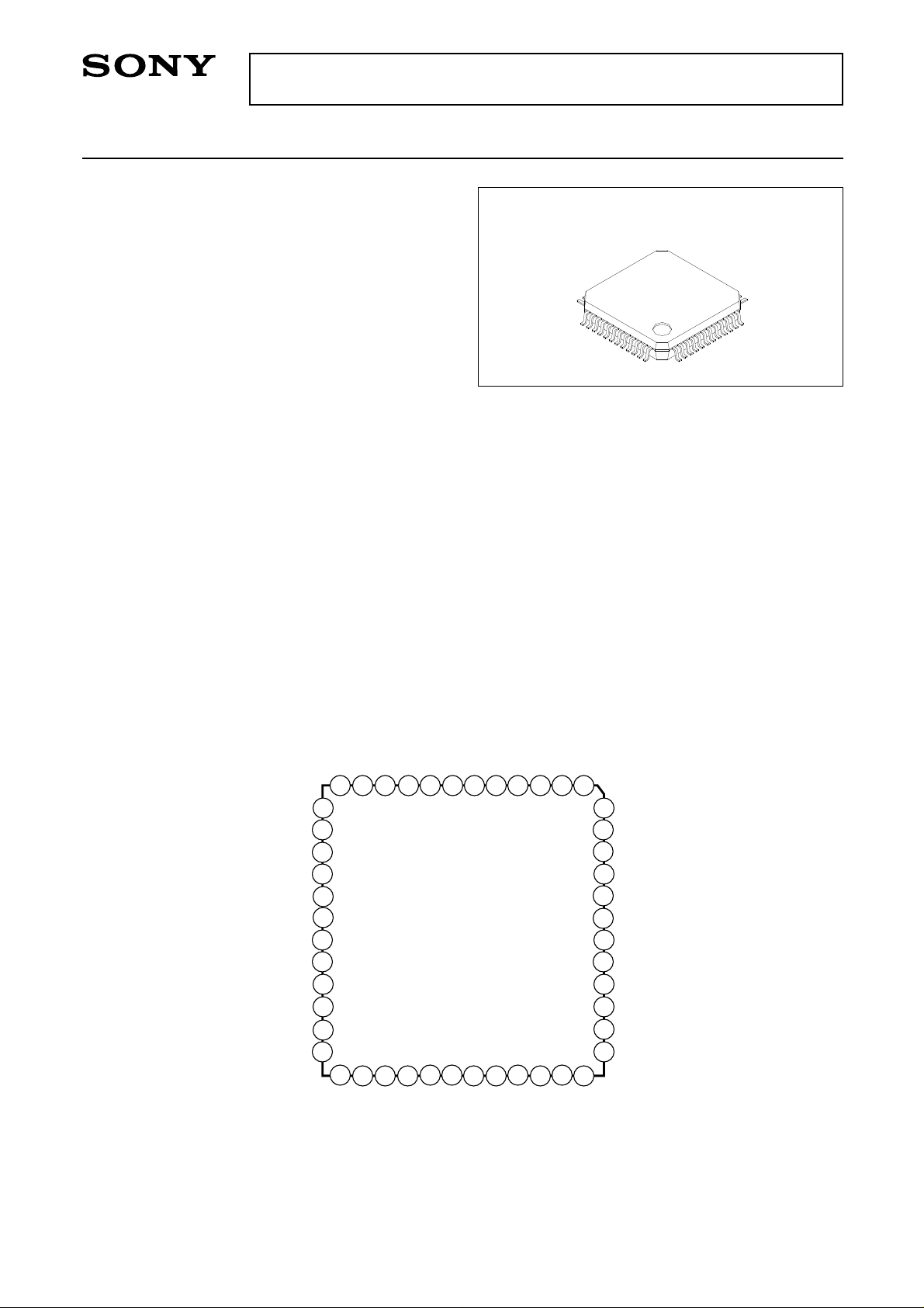
CXA3086Q
48 pin QFP (Plastic)
Structure
Bipolar silicon monolithic IC
Applications
• Magnetic recording (PRML)
• Communications (QPSK, QAM)
• LCDs
• Digital oscilloscopes
RESETN/T
RESET/E
9
10
27
28
CLK/T
2
CC
DV
29
2
CC
DV
DGND2
8
7
30
DGND2
P2D3
P2D4
P2D5 (MSB)
6
5
33
32
31
P1D2
P1D1
P1D0 (LSB)
P2D2
4
P1D3
3
34
P2D1
35
P1D4
DGND2
P2D0 (LSB)
2
48
47
46
45
44
43
42
41
40
39
38
37
36
DGND2
P1D5 (MSB)
DVCC2
DV
CC1
DGND1
N.C.
PS
CLKOUT
INV
SELECT
N.C.
DGND1
DVCC1
DV
CC2
Pin Configuration (Top View)
RESETN/E
12 1
11
13
DV
EE3
14
AGND
15
VRBS
16
V
RB
17
AVCC
18
N.C.
19
IN
V
20
AVCC
21
VRT
VRTS
22
23
AGND
DGND3
Sony reserves the right to change products and specifications without prior notice. This information does not convey any license by
any implication or otherwise under any patents or other right. Application circuits shown, if any, are typical examples illustrating the
operation of the devices. Sony cannot assume responsibility for any problems arising out of the use of these circuits.
24
25
CLK/E
26
CLKN/E
– 1 –
E95619C77
Page 2

CXA3086Q
Absolute Maximum Ratings (Ta = 25°C)
Unit
• Supply voltage AVCC, DVCC1, DVCC2 –0.5 to +7.0 V
DGND3 –0.5 to +7.0 V
DVEE3 –7.0 to +0.5 V
DGND3 – DVEE3 –0.5 to +7.0 V
• Analog input voltage VIN VRT – 2.7 to AVCC V
• Reference input voltage VRT 2.7 to AVCC V
VRB VIN – 2.7 to AVCC V
|VRT – VRB| 2.5 V
∗
• Digital input voltage ECL (∗∗∗/E
1
)DVEE3 to +0.5 V
PECL (∗∗∗/E) –0.5 to DGND3 V
TTL (∗∗∗/T, INV, PS) –0.5 to DVCC1V
other (SELECT) –0.5 to DVCC1V
VID∗2(|∗∗∗/E – ∗∗∗N/E|) 2.7 V
• Storage temperature Tstg –65 to +150 °C
• Allowable power dissipationPD 1.2 W
(when mounted on a glass fabric base epoxy board with 76mm x 114mm, 1.6mm thick)
Recommended Operating Conditions
With a single power supply With dual power supplies Unit
Min. Typ. Max. Min. Typ. Max.
• Supply voltage DVCC1, DVCC2, AVCC +4.75 +5.0 +5.25 +4.75 +5.0 +5.25 V
DGND1, DGND2, AGND –0.05 0 +0.05 –0.05 0 +0.05 V
DGND3 +4.75 +5.0 +5.25 –0.05 0 +0.05 V
DVEE3 –0.05 0 +0.05 –5.5 –5.0 –4.75 V
• Analog input voltage VIN VRB VRT VRB VRT V
• Reference input voltage VRT +2.9 +4.1 +2.9 +4.1 V
VRB +1.4 +2.6 +1.4 +2.6 V
|VRT – VRB| 1.5 2.1 1.5 2.1 V
• Digital input voltage ECL (∗∗∗/E) : VIH DGND3 – 1.05 DGND3 – 0.5 V
: VIL DGND3 – 3.2 DGND3 – 1.4 V
PECL (∗∗∗/E) : VIH DGND3 – 1.05 DGND3 – 0.5 V
: VIL DGND3 – 3.2 DGND3 – 1.4 V
TTL (∗∗∗/T, INV, PS): VIH 2.0 2.0 V
: VIL 0.8 0.8 V
other (SELECT) : VIH DVCC1DVCC1V
: VIL DGND1 DGND1 V
VID∗2(|∗∗∗/E – ∗∗∗N/E|) 0.4 0.8 0.4 0.8 V
• Maximum conversion rate Fc (Straight mode) 100 100 MSPS
(DMUX mode) 140 140 MSPS
• Ambient temperature Ta –20 +75 –20 +75 °C
∗1
∗∗∗/E and ∗∗∗/T indicate CLK/E and CLK/T, etc. for the pin name.
∗2
VID: Input Voltage Differential
ECL and PECL switching level
VID
– 2 –
DGND3
VIH (max.)
IL
V
VTH (DGND3 – 1.2V)
V
IH
V
IL (min.)
Page 3
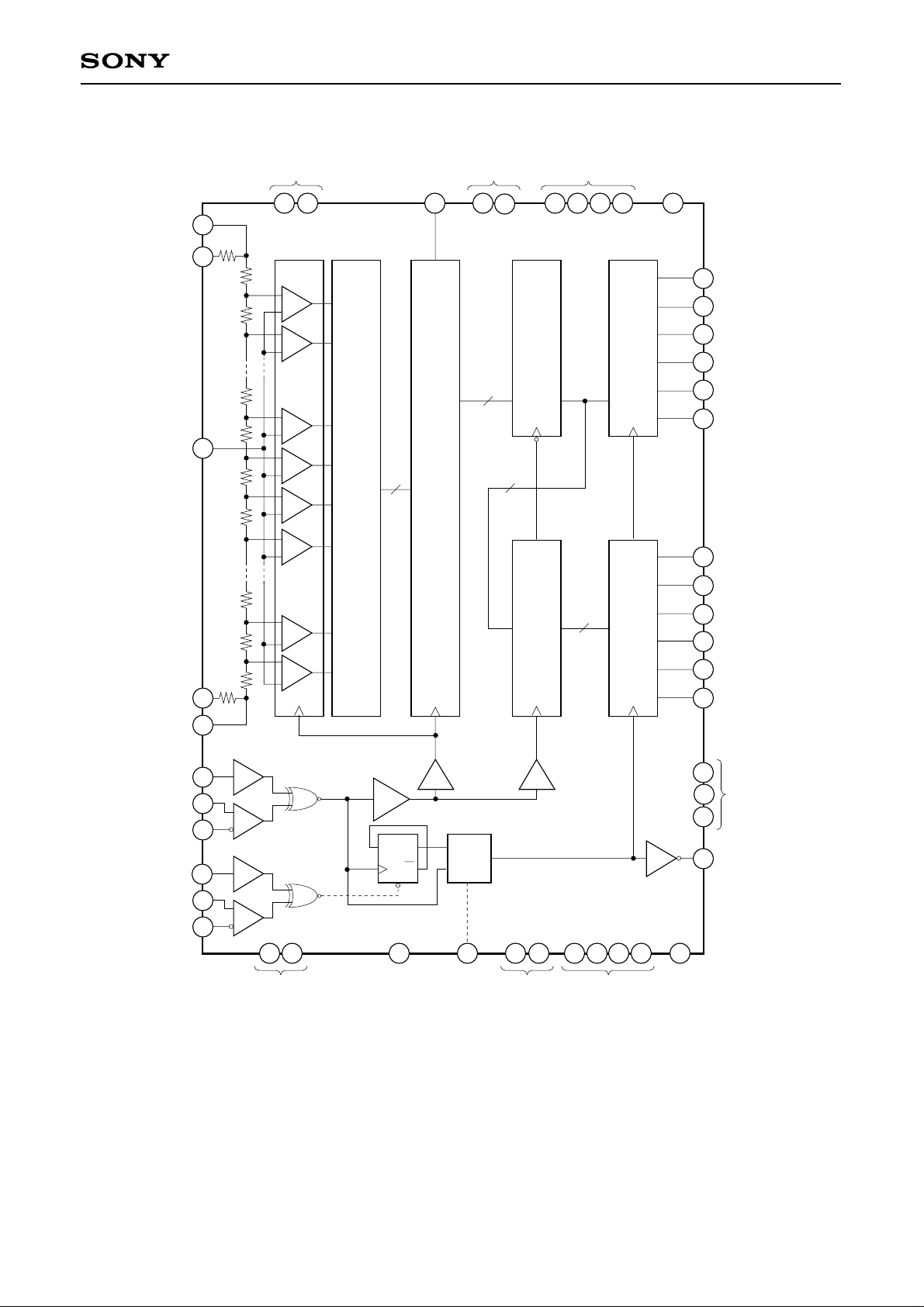
Block Diagram
CXA3086Q
VRTS
V
RT
VIN
VRB
VRBS
19
16
15
22
21
AVCC DVCC2
17
20
INV DGND3
42
DVCC1
38
47
37
9
28
48
24
r1
(MSB)
r
1
r
2
•
•
•
r
30
r
31
r
32
r
33
•
•
•
r
6bit
ENCODER
6bit
6bit LATCH
LATCHA
6bit
TTLOUT
6bit
62
r
r2
63
r
LATCHB
TTLOUT
35
34
33
32
31
30
7
6
5
4
3
2
P1D5
P1D4
P1D3
P1D2
P1D1
P1D0
(LSB)
(MSB)
P2D5
P2D4
P2D3
P2D2
P2D1
P2D0
(LSB)
CLK/T
CLK/E
CLKN/E
RESETN/T
RESETN/E
RESET/E
10
12
27
25
26
11
14
AGND
23
Delay
DQ
44
Q
Select
46
41
SELECTPS DVEE3
39
DGND1
1
DGND2
8
29
36
13
18
40
45
43
N.C.
CLKOUT
– 3 –
Page 4

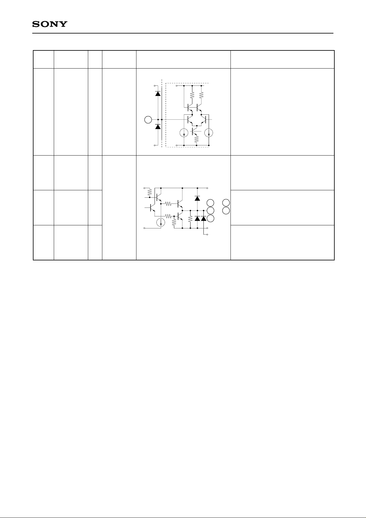
Pin Description and I/O Pin Equivalent Circuit
CXA3086Q
Pin
No.
14, 23
17, 20
1, 8,
29, 36,
39, 46
9, 28,
37, 38,
47, 48
24
Symbol
AGND
AVCC
DGND1
DGND2
DVCC1
DVCC2
DGND3
Standard
I/O
voltage level
GND
+5V
(typ.)
GND
+5V
(typ.)
+5V (typ.)
(With a
single
power
supply)
GND
(With dual
power
supplies)
Equivalent circuit Description
Analog ground.
Separated from the digital ground.
Analog power supply.
Separated from the digital power
supply.
Digital ground.
Digital power supply.
Digital power supply.
Ground for ECL input.
+5V for PECL and TTL input.
13
18, 40,
45
25
26
12
11
DVEE3
N.C.
CLK/E
CLKN/E
RESETN/E
RESET/E
GND
(With a
single
power
supply)
–5V (typ.)
(With dual
power
supplies)
I
I
ECL/
PECL
I
I
DGND3
12
11
DV
EE3
25
26
1.2V
r
r r
Digital power supply.
–5V for ECL input.
Ground for PECL and TTL input.
No connected pin.
Not connected with the internal
circuits.
Clock input.
CLK/E complementary input.
When left open, this pin goes to the
threshold potential.
Only CLK/E can be used for
r
operation, but complementary input
is recommended to attain fast and
stable operation.
Reset input.
When the input is set to low level,
the built-in CLK frequency divider
circuit can be reset.
RESETN/E complementary input.
When left open, this pin goes to the
threshold voltage. Only RESETN/E
can be used for operation.
– 4 –
Page 5

CXA3086Q
Pin
No.
Symbol I/O
27 CLK/T
10
RESETN/T
INV
42
44
PS
Standard
voltage level
I
TTL
I
I
TTL
I
Equivalent circuit Description
DVCC1
27
10
DGND1
DVEE3
r/2
1.5V
r
Clock input.
Reset input.
When left open, this input goes to
high level. When the input is set to
low level, the built-in CLK frequency
divider circuit can be reset.
Data output polarity inversion input.
DVCC1
When left open, this input goes to
high level.
(See Table 1. I/O Correspondence
Table.)
Power saving input.
42
44
When the input is set to low level,
the power saving mode is set.
In this time the all TTL outputs go
DGND1
DVEE3
into the high-impedance state.
Normally, set to high level or left
open.
SELECT
41
VRTS
22
21 VRT
VRB
16
15
VRBS
O
I
I
O
Vcc
or
GND
+4.0V
(typ.)
VRTS
+r1 x Iref
VRBS
–r2 x Iref
+2.0V
(typ.)
DVCC1
41
DGND1
DVEE3
22
21
16
15
Data output mode selection.
(See Table 2. Operating Mode
Table.)
Reference voltage sense.
1
r
r
Comparator 1
r
r
Comparator 2
r
r
Comparator 62
r
r
Comparator 63
r
2
r
By-pass to AGND with a 0.1µF chip
capacitor.
Top reference voltage.
By-pass to AGND with a 1µF tantal
capacitor and a 0.1µF chip
capacitor.
Bottom reference voltage.
By-pass to AGND with a 1µF tantal
capacitor and a 0.1µF chip
capacitor.
Reference voltage sense.
By-pass to AGND with a 0.1µF chip
capacitor.
– 5 –
Page 6
CXA3086Q
Pin
No.
Symbol I/O
19 VIN
P1D0
30
to
35
2
to
7
to
P1D5
P2D0
to
P2D5
43 CLKOUT
Standard
voltage level
I
O
O
O
VRT
to
VRB
TTL
AVCC
19
DVEE3
DVCC1
DGND1
Equivalent circuit Description
Comparator
AVCC
Analog input.
Vref
AGND
Port 1 side data output.
DVCC2
7
to
100k
2
30
43
DGND2
DVEE3
Port 2 side data output.
to
35
Clock output.
(See Table 2. Operating Mode Table.)
– 6 –
Page 7

Electrical Characteristics
(DVCC1, 2, AVCC, DGND3 = +5V, DGND1, 2, AGND, DVEE3 = 0V, VRT = 4V, VRB = 2V, Ta = 25°C)
Item Symbol Min. Typ. Max. UnitConditions
CXA3086Q
Resolution
DC characteristics
Integral linearity error
Differential linearity error
Analog input
Analog input capacitance
Analog input resistance
Analog input current
Reference input
Reference resistance
Reference current
Residual resistance r1
Digital input (ECL, PECL)
Digital input voltage: High
: Low
Threshold voltage
Digital input current: High
: Low
Digital input capacitance
Digital input (TTL)
Digital input voltage: High
: Low
Threshold voltage
Digital input current: High
: Low
Digital input capacitance
6
EIL
EDL
CIN
RIN
IIN
∗3
Rref
∗4
Iref
r1
r2
r2
VIH
VIL
VTH
IIH
IIL
VIN = 2Vp-p, Fc = 5MSPS
VIN = +3.0V + 0.07Vrms
VIH = DGND3 – 0.8V
VIL = DGND3 – 1.6V
16
0
160
6.5
3.0
3.0
DGND3 – 1.05
DGND3 – 3.2
DGND3 – 1.2
–50
–75
7
225
9.0
4.2
4.2
±0.2
±0.2
150
125
308
12.5
5.7
5.7
DGND3 – 0.5
DGND3 – 1.4
+50
0
5
VIH
VIL
VTH
IIH
IIL
VIH = 3.5V
VIL = 0.2V
2.0
–50
–500
0.8
1.5
0
0
5
bits
LSB
LSB
pF
kΩ
µA
Ω
mA
Ω
Ω
V
V
V
µA
µA
pF
V
V
V
µA
µA
pF
Digital output (TTL)
Digital output voltage
Leak current during output off
: High
: Low
VOH
VOL
IOZ
IOH = –2mA
IOL = 1mA
Power saving mode
Switching characteristics
Maximum conversion rate
Aperture jitter
Sampling delay
Clock high pulse width
Clock low pulse width
RESET Signal setup time
RESET Signal hold time
CLKOUT output delay
Data output delay
Output rise time
Output fall time
These characteristics are for PECL input, unless otherwise specified.
∗
Fc
Taj
Tds
Tpw1
Tpw0
T_rs
T_rh
Td_clk
Tdo1
Tdo2
Tr
Tf
DMUX mode
CLK
CLK
RESETN – CLK
RESETN – CLK
(CL = 5pF)
DMUX mode (CL = 5pF)
(CL = 5pF)
0.8 to 2.0V (CL = 5pF)
0.8 to 2.0V (CL = 5pF)
2.4
–15
140
3
2.9
2.9
3.5
0
4.5
∗5
T
6.5
10
4.5
7
T + 1
8
2
2
0.5
70
6
8
T + 2
10
V
V
µA
MSPS
ps
ns
ns
ns
ns
ns
ns
ns
ns
ns
ns
– 7 –
Page 8
Item Symbol Min. Typ. Max. UnitConditions
Dynamic characteristics
Input bandwidth
S/N ratio
Error rate
VIN = 2Vp-p, –3dB
Fc = 140MSPS,
fin = 1kHz Fs
{
DMUX mode
Fc = 140MSPS,
fin = 34.999MHz Fs
{
DMUX mode
Fc = 140MSPS,
fin = 1kHz Fs
DMUX mode
{
Error > 4LSB
Fc = 140MSPS,
fin = 34.999MHz Fs
DMUX mode
{
Error > 4LSB
Fc = 100MSPS,
fin = 24.999MHz Fs
straight mode
{
Error > 4LSB
200
37.0
34.5
10
10
10
–12
–9
–9
CXA3086Q
MHz
dB
dB
∗6
TPS
TPS
TSP
Power supply
Supply current
Supply current
Power consumption
Supply current
Power consumption
∗3
Rref: Resistance value between VRT and VRB
∗4
∗5
∗6
∗7
VIN
VRTS
VRBS
VRT – VRB
Iref =
T =
TPS: Times Per Sample
Pd = (ICC + IEE) · VCC +
Rref
1
Fc
Step
D5 D0 D5 D0
63
1 1 1 1 1 1
62
1 1 1 1 1 0
:
32
1 0 0 0 0 0
31
0 1 1 1 1 1
:
1
0 0 0 0 0 1
0
0 0 0 0 0 0
Table 1. I/O Correspondence Table
1
:
:
ICC
IEE
∗7
Pd
ICC + IEE
Pd
(VRT – VRB)
Rref
INV
0 0 0 0 0 0
0 0 0 0 0 1
0 1 1 1 1 1
1 0 0 0 0 0
1 1 1 1 1 0
1 1 1 1 1 1
Power saving mode
Power saving mode
2
0
:
:
Step
63
62
61
60
59
58
·
·
·
·
·
·
·
5
4
3
2
1
0
54.0
0.4
290
2.0
28
1LSB
r1 × Iref
V
RTSVRT VRBS VRB
67.5
VIN
0.6
360
90
0.8
470
8.0
58
mW
mW
r
2 × Iref
mA
mA
mA
– 8 –
Page 9
Electrical Characteristics Measurement Circuit
Current Consumption Measurement Circuit
CXA3086Q
Sampling Delay Measurement Circuit
Aperture Jitter Measurement Circuit
5V 5V
A A
4V
1.95V
2V
VRT
VIN
VRB
Icc
AVCC
DVCC1
DVCC2
DGND2
DGND1
AGND
DGND3
CLK/E
EE3
DV
I
EE
5MHz PECL
Integral Linearity Error Measurement Circuit
Differential Linearity Error Measurement Circuit
+V
S2
S1: ON when A < B
S1
S2: ON when A > B
100MHz
Amp
OSC1
φ: Variable
V
fr
OSC2
100MHz
IN
CXA3086Q
CLK
ECL
Buffer
6
Aperture Jitter Measurement Method
VIN
CLK
Logic
Analizer
1024
samples
VRT
VRB
–V
A < B A > B
Comparator
IN
DVM
V
CXA3086Q
6 6
A6
to
A1
A0
Controller
Error Rate Measurement Circuit
Signal
Source
C
F
– 1kHz
4
2Vp-p Sin Wave
VIN
CXA3086Q
CLK CLK
B6
B1
B0
∆υ
∆ t
IN
V
“1”“0”
Latch
Buffer
4LSB
00···0
to
11···0
CLK
Where σ (LSB) is the deviation of the output codes when
the largest slew rate point is sampled at the clock which
has exactly the same frequency as the analog input
signal, the aperture jitter Taj is:
Taj = σ/ = σ/ ( )
+
Latch
∆υ
∆t
A
B
Comparator
A > B
to
6
33
32
31
30
29
Sampling timing fluctuation
(= aperture jitter)
64
× 2πf
2
σ (LSB)
Pulse
Counter
Signal
Source
F
C
1/8
– 9 –
Page 10

Description of Operating Modes
The CXA3086Q has two types of operating modes which are selected with Pin 41 (SELECT).
CXA3086Q
Operating
mode
DMUX mode
Straight mode
SELECT
VCC
GND
Maximum
conversion rate
140MSPS
100MSPS
Data output Clock output
Demultiplexed output
70Mbps
Straight output
The input clock is 1/2 frequency divided
and output. 70MHz
The input clock is inverted and output.
100Mbps
100MHz
Table 2. Operating Mode Table
1. DMUX mode (See Application Circuits (1), (2) and (3).)
Set the SELECT pin to Vcc for this mode. In this mode, the clock frequency is divided by 2 in the IC, and the
data is output after being demultiplexed by this 1/2 frequency divided clock. The 1/2 frequency divided clock,
which has adequate setup time and hold time for the output data, is output from the CLKOUT pin.
When resetting this 1/2 frequency divided clock, the low level of the RESET signal should be input to the
RESETN pin (Pin 10 or 12). The RESET signal requires the setup time (T_rs ≥ 3.5ns) and hold time (T_rh ≥
0ns) to the clock rising edge because it is synchronized with and taken in the clock. Therefore, set the RESET
signal to low for T_rs (min.) + T_rh (min.) = 3.5ns or longer to the clock rising edge.
The reset period can be extended by making the low level period of the RESET signal longer because the
clock output pin is fixed to low (reset) during the low level period at the clock rising edge. If the reset start
timing is regarded as not important, the timing where the RESET signal is set from high to low is not so
consequence. However, when the reset is released this timing must become significant because the timing is
used to commence the 1/2 frequency divided clock. In this case, the setup time (T_rs) is also necessary.
See the timing chart for detail. (This chart shows the example of reset for 2T.)
The A/D converter can operate at FC (min.) = 140MSPS in this mode.
– 10 –
Page 11

A
A
A
When the RESET signal is not used.
CXA3086Q
CLK
CXA3086Q
CLK
CLK
A
AA
RESETN
CXA3086Q
B
CLK
RESETN
When the RESET signal is used.
CXA3086Q
A
CLK
RESET signal
CLK
RESETN
A
CXA3086Q
CLK
A
RESETN
B
CLKOUT
A
B
6bit
6bit
6bit
6bit
DATA
CLKOUT
DATA
CLK
RESET signal
CLKOUT
DATA
CLKOUT
DATA
(Reset period)
(Reset period)
2. Straight mode (See Application Circuits (4), (5) and (6).)
Set the SELECT pin to GND for this mode. In this mode, data output can be obtained in accordance with the
clock frequency applied to the A/D converter for applications which use the clock applied to the A/D converter
as the system clock.
The A/D converter can operate at Fc (min.) = 100MSPS in this mode.
Digital input level and supply voltage settings
The logic input level for the CXA3086Q supports ECL, PECL and TTL levels.
The power supplies (DVEE3, DGND3) for the logic input block must be set to match the logic input (CLK and
RESET signals) level.
Digital input level
ECL
PECL
TTL
DVEE3 DGND3 Supply voltage Application circuits
–5V
0V
0V
0V
+5V
+5V
±5V
+5V
+5V
(1) (4)
(2) (5)
(3) (6)
Table 3. Logic Input Level and Power Supply Settings
– 11 –
Page 12

Application Circuit 1
(1) DMUX ECL input
CXA3086Q
ECL RESET Signal
(2) DMUX PECL input
PECL RESET Signal
–5V (D)
AG
AG
+5V (A)
AG
+5V (A)
AG
AG
DG
ECL-CLK
DG
+5V (A)
+5V (A)
+5V (D)
PECL-CLK
+5V (D)
DG
6
9
12 1
10
11
13
14
15
2V
16
17
18
19
20
4V
21
22
23
24
26
27 28
25
+5V (D)
+5V (D)
9
12 1
10
11
13
AG
AG
AG
AG
AG
14
15
2V
16
17
18
19
20
4V
21
22
23
24
26 27
28
25
+5V (D)
5
8
29
DG
DG
8
29
DG
4
7
31
30
6
7
31
30
2
3
35
32
33
34
5
4
3
35
32
33
34
P2D0 to P2D5
DG
6 bit Digital
Data
48
47
46
45
44
43
42
41
40
39
38
37
+5V (D)
DG
+5V (D)
DG
+5V (D)
P1D0 to P1D5
6 bit Digital
Data
P2D0 to P2D5
6 bit Digital
Data
+5V (D)
DG
+5V (D)
DG
+5V (D)
P1D0 to P1D5
6 bit Digital
Data
48
47
46
45
44
43
42
41
40
39
38
37
36
DG
DG
2
36
DG
Latch
Latch
Latch
Latch
6 bit Digital Data
6 bit Digital Data
6 bit Digital Data
6 bit Digital Data
(3) DMUX TTL input
TTL RESET Signal
+5V (A)
+5V (A)
+5V (D)
TTL-CLK
+5V (D)
DG
6
9
12 1
10
DG
AG
AG
AG
AG
AG
11
13
14
15
2V
16
17
18
19
20
4V
21
22
23
24
26
27 28
25
+5V (D)
5
8
29
DG
4
7
31
30
2
3
35
32
33
34
P2D0 to P2D5
DG
6 bit Digital
Data
48
47
46
45
44
43
42
41
40
39
38
37
36
DG
+5V (D)
DG
+5V (D)
DG
+5V (D)
P1D0 to P1D5
6 bit Digital
Data
Latch
Latch
6 bit Digital Data
6 bit Digital Data
– 12 –
Page 13

(4) Straight ECL input
CXA3086Q
(5) Straight PECL input
–5V (D)
AG
AG
+5V (A)
AG
+5V (A)
AG
AG
DG
ECL-CLK
DG
AG
AG
+5V (A)
AG
+5V (A)
AG
AG
+5V (D)
PECL-CLK
+5V (D)
DG
9
12 1
10
8
+5V (D)
+5V (D)
10
27
+5V (D)
28
29
DG
ECL TTL
DG
9
28
29
DG
7
31
30
8
7
30
11
13
14
15
2V
16
17
18
19
20
4V
21
22
23
24
26 27
25
12 1
11
13
14
15
2V
16
17
18
19
20
4V
21
22
23
24
26
25
DG
6
5
4
2
3
48
47
46
45
44
43
42
41
40
39
38
37
35
32
6
5
32
31
36
33
34
DG
DG
4
2
3
46
35
36
33
34
DG
48
47
45
44
43
42
41
40
39
38
37
+5V (D)
DG
+5V (D)
DG
DG
+5V (D)
P1D0 to P1D5
6 bit Digital
Data
+5V (D)
DG
+5V (D)
DG
DG
+5V (D)
P1D0 to P1D5
6 bit Digital
Data
Latch
Latch
6 bit Digital Data
6 bit Digital Data
(6) Straight TTL input
+5V (A)
+5V (A)
+5V (D)
TTL-CLK
PECL TTL
+5V (D)
DG
6
DG
AG
AG
AG
AG
AG
13
14
15
2V
16
17
18
19
20
4V
21
22
23
24
26
27 28
25
+5V (D)
9
12 1
10
11
5
8
7
32
31
30
29
DG
DG
4
2
3
48
47
46
45
44
43
42
41
40
39
37
35
36
33
34
DG
38
+5V (D)
DG
+5V (D)
DG
DG
+5V (D)
P1D0 to P1D5
6 bit Digital
Data
Latch
6 bit Digital Data
– 13 –
Page 14

Application Circuit 2 Straight Mode TTL I/O (When a single power supply is used)
AG
VRTS
4V
DG
1µF
short
Analog
input
AG AG
+5V
(A)
10µF
AG AG
1µF
2V
short
CXA3086Q
VRBS
TTL CLK
(LSB)
(MSB)
P1D0
P1D1
P1D2
P1D3
P1D4
P1D5
25
26
27
28
29
30
31
32
33
34
35
36
CLK/E
CLKN/E
CLK/T
DV
CC2
DGND2
P1D0
P1D1
P1D2
P1D3
P1D4
P1D5
DGND2
24
DGND3
2
CC
DV
37
23
AGND
38
1
CC
DV
22
RTS
V
DGND1
39
40
21
RT
V
N.C.
20
CC
AV
SELECT
41
19
42
IN
V
INV
18
N.C.
CLKOUT
43
17
44
CC
AV
PS
16
45
RB
V
N.C.
RBS
V
DGND1
46
1415
AGND
1
CC
DV
47
13
3
EE
DV
RESETN/E
RESET/E
RESETN/T
DV
CC2
DGND2
P2D5
P2D4
P2D3
P2D2
P2D1
P2D0
DGND2
2
CC
DV
48
12
10
11
5
9
8
7
6
P2D5
P2D4
(MSB)
P2D3
4
3
2
P2D2
P2D1
P2D0
(LSB)
1
10µF
DG
+5V
(D)
CLKOUT
Short the analog system and digital system at one point immediately under the A/D converter.
See the Notes on Operation.
is the chip capacitor of 0.1µF.
Application circuits shown are typical examples illustrating the operation of the devices. Sony cannot assume responsibility for
any problems arising out of the use of these circuits or for any infringement of third party patent and other right due to same.
– 14 –
Page 15

DMUX Mode Timing Chart (Select = VCC)
CXA3086Q
Tds
4.5ns (typ.)
V
IN
CLK
P1D0 to D5 N + 1 N + 3
P2D0 to D5 N
CLK OUT
N – 1
N + 3
N
T
Tpw0Tpw1
T_rhT_rsT_rh
N + 1
(Reset period)
T_rs
N + 2
Td_clk;
7ns (typ.)
8ns (max.)
4.5ns (min.)
2.0V
0.8V
4.5ns (min.)
8ns (max.)
Td_clk
N + 4
2.0V
0.8V
N + 5
Tdo2;
8ns (typ.)
6.5ns (min.)
10ns (max.)
Tdo1
T + 1ns (typ.)
2.0V
0.8V
2.0V
0.8V
2.0V
0.8V
≈T
N + 6
N + 2
N + 7
≈T
RESET signal
– 15 –
Page 16

Straight Mode Timing Chart (Select = GND)
CXA3086Q
V
CLK
P1D0 to D5 NN – 2N – 4
P2D0 to D5
(CLK is inverted and output.)
CLK OUT
N – 1
IN
Tds
4.5ns (typ.)
T
Tpw1
Tdo2; 8ns (typ.)
6.5ns (min.)
10ns (max.)
Td_clk; 7ns (typ.)
4.5ns (min.)
8ns (max.)
Tpw0
2.0V
0.8V
2.0V
0.8V
2.0V
0.8V
N
N – 3 N – 1
N – 4 N – 2 N – 1N – 3N – 5
N + 1
N + 2
N + 3
RESET signal
– 16 –
Page 17

CXA3086Q
Timing of A/D Converter and Peripheral Circuit
In the maximum clock rate of the DEMUX Mode, the timing of 3 channels of ADC CLK OUT in same phase is
described in detail as below.
For example, the CLK OUT from one of the ADC is used as the data latch clock. The clock delay and data
delay are showed in the following specification, i.e.
Td_clk 4.5ns (min.) to 8.0ns (max.)
Tdo2 6.5ns (min.) to 10ns (max.)
These values are considered in all the temperature change and power supply variation. When the maximum
clock rate 140MSPS is used, the set-up time (ts) is seemed to be very small from above specifications. But the
3 channels of ADC are in the same circuit board, so that the DATA OUT delay and CLK OUT delay will be
changed in same trend at the same condition of the temperature change and power supply variation. As a
result, 0.5ns of the delay will be faster, when the highest temperature and highest power supply is used. Also,
0.5ns of the delay will be later, when the lowest temperature and lowest power supply is used. These delay
can be omitted in this case.
When Ta = 25°C, VCC = +5V, the clock delay and data delay are
Td_clk 5.0ns (min.) to 7.5ns (max.)
Tdo2 7.0ns (min.) to 9.5ns (max.)
The timing of the DATA OUT and CLK OUT with above delay variation is showed in below. Consequently, the
set-up time for the data latching can be obtained as ts (min.) = 2.5ns. The output delay change of the DATA OUT
and CLK OUT due to the temperature change and the power supply variation should have the same trend of
the delay change, the minimum ts = 2.5ns can be guaranteed at any temperature change and power supply
variation.
Analog input R
CXA3086Q
Vin
CLK
RESET
P1D/out
P2D/out
CLK OUT
6bit
6bit
Gate Array
Latch
Analog input G
Analog input B
RESET
CLK
RESET signal
CLK OUT
P1D/out
P2D/out
CLK
CXA3086Q
Vin
CLK
RESET
CXA3086Q
Vin
CLK
RESET
( = 1/140MSPS)
th-reset
P1D/out
P2D/out
CLK OUT
P1D/out
P2D/out
CLK OUT
7ns
Td_clk (min.)
5.0ns
<4.5ns>
Td_clk (max.)
7.5ns
<8.0ns>
6bit
6bit
6bit
6bit
Tdo2 (min.)
7.0ns
<6.5ns>
Tdo2 (min.)
9.5ns
<10ns>
ts (min.)
2.5ns
th (min.)
6.5ns
14ns
Note: In the timing chart, the values in the brackets < > are included all the temperature change and the
power supply variation.
– 17 –
Page 18

CXA3086Q
Notes on Operation
• The CXA3086Q is a high-speed A/D converter which is capable of TTL, ECL and PECL level clock input.
Characteristic impedance should be properly matched to ensure optimum performance during high-speed
operation.
• The power supply and grounding have a profound influence on converter performance. The power supply
and grounding method are particularly important during high-speed operation. General points for caution are
as follows.
— The ground pattern should be as large as possible. It is recommended to make the power supply and
ground patterns wider at an inner layer using a multi-layer board.
— To prevent interference between AGND and DGND and between AVcc and DVcc, make sure the
respective patterns are separated. To prevent a DC offset in the power supply pattern, connect the AVcc
and DVcc lines at one point each via a ferrite-bead filter Shorting the AGND and DGND patterns in one
place immediately under the A/D converter improves A/D converter performance.
— Ground the power supply pins (AVcc, DVcc1, DVcc2, DVEE3) as close to each pin as possible with a
0.1µF or larger ceramic chip capacitor.
(Connect the AVcc pin to the AGND pattern and the DVcc1, DVcc2 and DVEE3 pins to the DGND pattern.)
— The digital output wiring should be as short as possible. If the digital output wiring is long, the wiring
capacitance will increase, deteriorating the output slew rate and resulting in reflection to the output
waveform since the original output slew rate is quite fast.
• The analog input pin VIN has an input capacitance of approximately 7pF. To drive the A/D converter with
proper frequency response, it is necessary to prevent performance deterioration due to parasitic capacitance
or parasitic inductance by using a large capacity drive circuit. keeping wiring as short as possible, and using
chip parts for resistors and capacitors, etc.
• The VRT and VRB pins must have adequate by-pass to protect them from high-frequency noise. By-pass them
to AGND with an approximately 1µF tantal capacitor and 0.1µF chip capacitor as short as possible.
• The offset for residual resistance is generated each for the reference voltage pins VRT and VRB.
When the offset voltage has no influence on the IC operation, the voltage should be applied to the VRT and
VRB pins directly, keeping the VRBS pin open. When the reference voltage is to be supplied to these pins
precisely, form the feedback loop circuit with VRT and VRB as a force pin and adjust the offset voltage to be
0V. See the “Application Circuit 2” for details.
• If the CLKN/E pin is not used, by-pass this pin to DGND with an approximately 0.1µF capacitor. At this time,
approximately DGND3 – 1.2V voltage is generated. However, this is not recommended for use as threshold
voltage VBB as it is too weak.
• When the digital input level is ECL or PECL level, ∗∗∗/E pins should be used and ∗∗∗/T pins left open. When
the digital input level is TTL, ∗∗∗/T pins should be used and ∗∗∗/E pins left open.
– 18 –
Page 19

Example of Representative Characteristics
CXA3086Q
Current consumption vs.
Ambient temperature characteristics
70
65
60
55
Current consumption [mA]
50
–25
Ta – Ambient temperature [°C]
Analog input current vs.
Analog input voltage characteristics
25 75
Current consumption vs.
Conversion rate characteristics
90
80
70
60
Current consumption [mA]
50
0
Fc – Conversion rate [MSPS]
Reference current vs.
Ambient temperature characteristics
11
CLK
f
fin = – 1kHz
4
DMUX mode
CL = 5pF
70
140
100
10
VRT = 4V
VRB = 2V
9
50
8
Analog input current [µA]
0
234
Analog input voltage [V]
Reference current [mA]
7
–25 25 75
Ta – Ambient temperature [°C]
– 19 –
Page 20

CXA3086Q
40
35
SNR [dB]
30
180
170
SNR vs. Input frequency response
Fc = 140MSPS
1
550
30310
Input frequency [MHz]
Maximum conversion rate vs.
Ambient temperature characteristics
CLK
f
fin = – 1kHz
4
Error > 4LSB
Error rate: 10–9TPS
100
Error rate vs. Conversion rate characteristics
–6
10
f
CLK
fin = – 1kHz
–7
10
–8
10
Error rate [TPS]
–9
10
–10
10
4
Error > 4LSB
140 160 200
180
Fc – Conversion rate [MSPS]
160
150
Fc – Maximum conversion rate [MSPS]
140
–25
25 75
Ta – Ambient temperature [°C]
– 20 –
Page 21

CXA3086Q
CXA3086Q Evaluation Board
Description
The CXA3086Q Evaluation Board is a special board designed to maximize and facilitate the evaluation
performance of the CXA3086Q. After latching the CXA3086Q output data with a frequency divided clock, the
analog signal can be regenerated by a 10-bit high-speed D/A converter. The latched data can also be
extracted externally via a 24-pin cable connector.
Features
• Resolution: 6 bits
• Maximum conversion rate: 140MSPS (min.)
• Supply voltage: ±5.0V
• Dual analog input pins: DIR.IN: AC coupling input pin
AMP.IN: Operational amplifier input pin
• Clock frequency division: 1/1 to 1/16
Absolute Maximum Ratings
• Supply voltage VCC –0.5 to +7.0 V
VEE –7.0 to +0.5 V
Recommended Operating Conditions Min. Typ. Max.
• Supply voltage VCC +4.75 +5.0 +5.25 V
GND 0 V
VEE –5.25 –5.0 –4.75 V
• Analog input AMP. IN –0.75 0 +1.05 V
DIR. IN 1.5 2.0 2.2 Vp-p
• Clock input CLK. IN 0.8 1.0 1.2 Vp-p
– 21 –
Page 22

(–1.0V)
D/A OUT
FULL SCALE. R5
P2 side OUT
CXA3086Q
P1 side OUT
FULL SCALE. R4
D/A
INV
INV
NORM
PS
PS
NORM
A/D
INV
INV
NORM
SELECT
DMUX
Straight
(–1.0V)
D/A OUT
SW4
SW3
SW2
SW1
CON4
6
6
6
AGND
DAC
(ECL)
TTL/ECL
(TTL)
LATCH
(TTL)
P2D0 to D5
RT
V
P1D0 to D5
CXA3086Q
VRB
VIN
CON5
DAC
6
(ECL)
6
(TTL)
LATCH
6
(TTL)
CLK CLKOUT
AGND
TTL/ECL
4
(ECL)
TTL/ECL
(TTL)
S2
(TTL)
PECL/TTL
CON8 CON7
P1 side DATA P2 side DATA
Block Diagram
OFFSET. R3
VRT. R2
VRB. R1
OFFSET
Vrt
Vrb
CON2
DIR IN
51Ω
Vrt
270Ω
AGND
AGND
A
130Ω
CON1
B
× (–2)
82Ω
AMP IN
– 22 –
Vrb S1
AGND
AGND
AGND
(PECL)
VBB
1kΩ 390Ω
CON3
0.1µF
51Ω
CLK IN
1kΩ
DGND
DGND
4
(PECL)
Counter
EE GND VCC
V
CON6
Page 23

Pin Description and I/O Level
CXA3086Q
Pin No.
CON1
CON2
CON3
CON4
CON5
CON6
CON7
Symbol I/O
AMP. IN
DIR. IN
CLK. IN
P2 side OUT
P1 side OUT
VCC
GND
VEE
P2 side DATA
I
I
I
O
O
I
I
I
O
Standard
I/O level
0.95Vp-p
2.0Vp-p
1.0Vp-p
0 to –1V
0 to –1V
+5.0V
0V
–5.0V
TTL
Current Description
Doubles the analog input signal amplitude using the
operational amplifier. The input impedance is 50Ω.
AC coupling input. Suitable for sine waves and other
repeating waveforms. The input impedance is 50Ω.
The CXA3086Q operates at the PECL level clock
using the sine wave-to-PECL conversion circuit.
The input impedance is 50Ω.
Allows the D/A converted waveform of the
CXA3086Q port 2 side data to be observed.
The output impedance is 50Ω.
Allows the D/A converted waveform of the
CXA3086Q port 1 side data to be observed.
The output impedance is 50Ω.
0.8A
The inside of the board is divided into analog and
digital systems.
–0.6A
The CXA3086Q port 2 side data output is latched at
the frequency divided clock and then output.
CON8
P1 side DATA
O
TTL
The CXA3086Q port 1 side data output is latched at
the frequency divided clock and then output.
Board Adjustments and Settings
1. VRB.R1: CXA3086Q VRB voltage adjusting volume.
2. VRT.R2: CXA3086Q VRT voltage adjusting volume.
3. OFFSET.R3: Adjusting volume for matching the AMP.IN input and DIR.IN input signal ranges to the
CXA3086Q input range.
4. FULL SCALE.R4: Full-scale adjusting volume for the port 2 D/A output. (–1V: Typ.)
5. FULL SCALE.R5: Full-scale adjusting volume for the port 1 D/A output. (–1V: Typ.)
6. S1: Switching junction for the dual analog input pins.
Set as follows according to the input pins used.
Junction
Symbol
AMP.IN
DIR.IN
AB
OPEN
0.1µF
SHORT
10kΩ
7. S2: Setting junction for the clock frequency division ratio. The operating speed after
latching is determined by the frequency division ratio set here.
When set to CLK OUT, it operates according to the CXA3086Q clock output.
8. SW1 SELECT: CXA3086Q output mode selector switch.
9. SW2 A/D INV: CXA3086Q output polarity inversion switch.
10. SW3 PS: CXA3086Q PS switch.
11. SW4 D/A INV: D/A converter output polarity inversion switch.
– 23 –
Page 24

Notes on Board Operation
1. The factory settings for the CXA3086Q Evaluation Board are as follows.
CXA3086Q
VRB.R1 = 1.5V
VRT.R2 = 3.0V
FULL SCALE.R4 = –1V
FULL SCALE.R5 = –1V
S1 A : OPEN, B : SHORT
S2 8 : SHORT (1/8 frequency division)
OFFSET.R3 = 2.25V
When using the board in this condition, the input signals should be input at the amplitudes shown below.
(The frequency is set as desired.)
Analog input signal: CON1 (AMP.IN)
Clock input signal: CON3 (CLK.IN)
0V center, 800mVp-p or less
0V center, 1.0Vp-p
2. When the analog signal is input from the CON1 (AMP.IN) pin, IC2:CLC404 limits the input dynamic range
of the A/D converter's analog input signal.
3. When the analog input signal is a sine wave or other repeating waveform, the signal can be input from the
CON2 (DIR.IN) pin with AC coupling. In these cases, the input dynamic range is not limited, but the VRT
level may be limited by IC3: NJM3403A.
4. In the evaluation board of the CXA3086Q, CLC404 (Comlinear) is employed for IC2 to drive the analog
input signal. Though, CLC505 (Comlinear) can also be used instead of CLC404, there should be a little
change in the peripheral circuit in this case.
– 24 –
Page 25

CXA3086Q Evaluation Board Timing Chart
CXA3086Q
CON2
DIR IN
CON3
CLK IN
CXA3086Q
CLK
CXA3086Q
P1 side DATA
(PECL)
(TTL)
N
N + 1
2Vp-p
1Vp-p
N – 4 N – 3 N – 2 N – 1
0V
0V
N + 2
N + 3
CON8
P1 side DATA
CLK
CON8
P1 side DATA
DATA
CON5
P1 side OUT
Operating Conditions CXA3086Q operating mode
Analog input
S2 setting
Approximately 6.0ns
(TTL)
N – 6
(TTL)
N – 6
(Analog regeneration waveform)
0 to –1V
Approximately 9.0ns
N – 2N – 4
N – 4
N – 2
: Straight mode
: DIR IN pin input
: 1/2 frequency divided clock
– 25 –
Page 26

Circuit Diagram
CXA3086Q
D1
TL431CP
AGND
AVCC
CON6
L1 L2 L3 L4 L5 L6
C1
33µFC233µF
AVEE DVEE AGND DGND AVCC DVCC
AGND AVEE
C5
1µF
R7
510
R1
2k
R8
510
R2
1k
R6
51
R3
10k
AMP IN
R9
7.5k
R10
22k
CON1
AGND
CLK IN
200k
C7
1µF
R11
AGND
AGND
AGND AVCC
CON3
DGND
C14
0.1µF
R13
82
C16
0.1µF
DGND
2
3
R19
1µF
11
1
4
NJM3403A
R14
130
1µF
C13
0.1µF
51
C6
390k
IC3A
C8
R12
AGND AVEE
C15
0.1µF
R15
270
2
3
AGND
C17
0.1µF
AGND AVCC
R201kR21
390
11
IC4D
10H116 (PECL)
AGND
CON2
DIR IN
AGND
R16
270
4
6
IC2
7
CLC404
IC4B
10H116 (PECL)
10
9
R22
1k
C3
33µF
IC3B
NJM3403A
6
5
R17
43
IC3C
NJM3403A
10
9
7
6
R18
VCCGNDVEE
DVCC
EE3
DV
AGND
RBS
V
VRB
AVCC
N.C.
IN
V
AVCC
VRT
VRTS
AGND
DGND3
R25 130 R28 82
R26 130 R29 82
R27 130 R30 82
DGND
DGND
DVCC
12
11
RESETN/E
CLK/E
26 27 28
25
10
RESET/E
RESETN/T
CLK/T
CLKN/E
DVCC
C24
0.1µF
9
CC2
DV
2
CC
DV
C23
0.1µF
SELECT
8
7
DGND2
CXA3086Q
DGND2
30
29
DVCC
SW4
D/A INV
SW3
PS
SW2
A/D INV
SW1
6
P2D5
IC1
P1D0
31
DGND
5
P2D4
P1D1
32
DGND
P2D3
P1D2
33
4
13
12
11
P2D2
P1D3
9
7
6
5
34
3
CLK
S1
S2
D0
D1
D2
D3
P2D1
P1D4
35
2
P2D0
P1D5
DGND
1
DGND2
DVCC2
DV
DGND1
N.C.
CLKOUT
SELECT
N.C.
DGND1
DV
DV
DGND2
36
DGND
IC5
10H136 (PECL)
CC1
PS
INV
CC1
CC2
C4
33µF
DGND
AGND
7
C18
C9
0.1µF
DVCC
DGND
1µF
AV
CC
CC
AV
C10
1µF
AGND
10H116 (PECL)
5
4
IC4A
C21
0.1µF
DVCC
3
2
51
A
B
S1
8
R23
82
R24
130
C19
0.1µF
C20
0.1µF
DGND
10H116 (PECL)
13
12
C27
0.1µF
IC4C
13
14
15
16
17
18
19
20
21
22
23
24
15
14
48
47
46
45
44
43
42
41
40
39
38
37
Cout
Q3
Q2
Q1
Q0
C28
0.1µF
0.1µF
C26
0.1µF
C27
0.1µF
C25
15
14
DGND
DGND
4
3
2
DAINV
ADINV
SELECT
P2D5
P2D4
P2D3
P2D2
P2D1
P2D0
DVCC
DGND
CLKOUT
ADINV
SELECT
DGND
DV
P1D5
P1D4
P1D3
P1D2
P1D1
P1D0
1/16
PS
PS
CC
1/8
1/4
1/2
– 26 –
CLK
CLKN
Page 27

DGND
C31
0.1µF
P2D5
P2D4
P2D3
P2D2
P2D1
P2D0
P1D5
P1D4
P1D3
P1D2
P1D1
P1D0
DAINV
CLKOUT
1/16
1/8
1/4
1/2
CLK
CLKN
DVCC
DGND
IC14
74ALS541
911
DGND
OC
1
CLK
11
1D 1Q
2
2D 2Q
3
3D 3Q
4
4D 4Q
5
5D 5Q
6
6D 6Q
7
7D 7Q
8
8D 8Q
9
DGND
OC
1
CLK
11
1D 1Q
2
2D 2Q
3
3D 3Q
4
4D 4Q
5
5D 5Q
6
6D 6Q
7
7D 7Q
8
8D 8Q
9
DGND
R51
620
R31 82 R34 130
R32 82 R35 130
R33 82 R36 130
DGND
IC6
74AS574
IC7
74AS574
19
17
24
1
23
22
21
20
16
15
14
13
12
11
OE
V
D0
D0N
D1
D1N
D2
D2N
D3
D3N
D4
D4N
D5
D5N
CXA3086Q
DVccDGND
1
17
16
15
14
13
12
IC9
100324
IC10
100324
IC11
10H124
25
C43
0.1µF
2
26
NQ5
NQ4
NQ3
NQ0
NQ1
NQ2
NQ5
NQ4
NQ3
NQ0
NQ1
NQ2
DVCC
DGND
CON7
P2 side DATA
14
Q5
13
12
Q4
11
9
Q3
10
24
Q0
1
2
Q1
3
5
Q2
4
14
Q5
13
12
Q4
11
9
Q3
10
24
Q0
1
2
Q1
3
5
Q2
4
2
Y1
4
1
Y2
3
Y2
15
Y3
12
Y3
14
Y4
13
Y4
1
DVEE
DVEE
DGND
DVEE
2
25
26
C47
0.1µF
C44
0.1µF
C46
0.1µF
0.1µF
DGND
C45
DVEE
DGND
P1 side DATA
R48
620
R37
R38
R50
620
CON8
R47
620
1
MSB
2
3
4
5
D5
6
D6
7
D7
8
D8
9
D9
10
LSB
11
NC
12
NC
13
R40
130
R39
130
14
10
11
12
13
14
R46
CLKN
CLK
DV
EE
1
MSB
2
D2
3
D3
4
D4
5
D5
6
D6
7
D7
8
D8
9
D9
LSB
NC
NC
CLKN
CLK
620
DVEE
82
82
R49
620
IC12
CX20201-1
IC13
CX20201-1
AGND
VREFD2
AV
NCD4
NC
NC
NC
NC
OUT
NC
AGND
DGND
INV
DV
AGND
VREF
AV
NC
NC
NC
NC
NC
OUT
NC
AGND
DGND
INV
DV
C51
28
0.1µF
27
26
EED3
25
24
C52
23
0.1µF
22
21
20
19
18
17
16
0.1µF
15
EE
C54
28
0.1µF
27
26
EE
25
24
0.1µF
23
22
21
20
19
18
17
16
15
EE
C50
0.1µF
R41
620
DVEE
C53
C55
C56
0.1µF
R4
2k
R5
2k
AGND
AGND
DGND
AGND
R421kR43
C11
AVEE
1µF
CON4
P2 side OUT
AGND
DGND
DVEE
AGND
R441kR45
C12
1µF
AVEE
CON5
P1 side OUT
AGND
DGND
DVEE
270
D2
TL431CP
270
D3
TL431CP
C42
0.1µF
IC15
74ALS541
17
3
P2D5
P2D4
P2D3
P2D2
P2D1
P2D0
19
18
P2D5
17
P2D4
16
P2D3
15
P2D2
14
P2D1
13
P2D0
12
19
18
17
16
15
14
13
12
BB
2
Q0
3
Q1
IC8
100390
4
Q2
8
Q3
9
Q4
10
Q5
CLKOUT
1/16
1/8
1/4
1/2
1/1
S2
P1D5
P1D4
P1D3
P1D2
P1D1
P1D0
16
4
15
5
6
14
13
7
12
8
DGND
DVCC
19
E
15
5D
16
4D
17
3D
21
0D
22
1D
23
2D
DVCC
19
E
15
5D
16
4D
17
3D
21
0D
22
1D
23
2D
6
B
5
A1 Y1
7
A2
10
A3
11
A4
IC14
74ALS541
P1D5
3
P1D4
4
P1D3
5
P1D2
6
P1D1
7
P1D0
8
– 27 –
Page 28

Component List
CXA3086Q
No. Product name Function
IC1 CXA3086Q 6-bit A/D converter
IC2 CLC404AJE OP-AMP
IC3 NJM3403AM OP-AMP
IC4 MC10H116L ECL Buffer
IC5 MC10H136L ECL Countor
IC6, 7 74AS574N TTL Latch
IC8 100390 PECL→TTL conversion
IC9, 10 100324PC TTL→ECL conversion
IC11 MC10H124L TTL→ECL conversion
IC12, 13 CXA20201A-1 10-bit D/A converter
IC14, 15 74ALS541N TTL Buffer
D1 to 3 TL431CP Shunt regulator
SW1 to 4 ATE1D-2F3-10 Toggle switch
S1, 2 JX-1 Short pin
CON1 to 5 01K0315 BNC connector
CON6 TJ-563 Power supply connector
CON7, 8 (FAP-2601-1202) Flat cable connector
L1 to 6 ZBF503D-00 Ferrite-bead filter
C1 to 4 Tantal capacitor 33µF
C5 to 12 Tantal capacitor 1µF
C13 Ceramic capacitor 0.1µF
All parts other than those listed above
Chip capacitor 0.1µF
No. Product name Function
R2 RJ-5W-1K 1kΩ volume resistor
R1, 4, 5 RJ-5W-2K 2kΩ volume resistor
R3 RJ-5W-10K 10kΩ volume resistor
R47 to 51 RGLD4X621J 620Ω network resistor
R6, 18, 19 FRD-25SR (0.25W) 51Ω
R7.8 FRD-25SR (0.25W) 510Ω
R9 FRD-25SR (0.25W) 7.5kΩ
R10 FRD-25SR (0.25W) 22kΩ
R11 FRD-25SR (0.25W) 200kΩ
R12 FRD-25SR (0.25W) 390kΩ
R13, 23, 28 to 33, 37, 38 FRD-25SR (0.25W) 82Ω
R14, 24 to 27, 34 to 36, 39, 40 FRD-25SR (0.25W) 130Ω
R15, 16, 43, 45 FRD-25SR (0.25W) 270Ω
R17 FRD-25SR (0.25W) 43Ω
R20, 22, 42, 44 FRD-25SR (0.25W) 1kΩ
R21 FRD-25SR (0.25W) 390Ω
R41, 46 FRD-25SR (0.25W) 620Ω
∗
CON7 and 8 are not mounted when boards are shipped. (Manufacturer: YAMAICHI Electronics Co., Ltd.)
Component side silk diagram
– 28 –
Page 29

CXA3086Q
Component side pattern diagram
Solder side pattern diagram
– 29 –
Page 30

Package Outline Unit: mm
CXA3086Q
48PIN QFP (PLASTIC)
15.3 ± 0.4
37
48
+ 0.4
12.0 – 0.1
2536
24
13
112
0.8 0.3 – 0.1
+ 0.15
± 0.12
M
+ 0.35
2.2 – 0.15
+ 0.1
0.15 – 0.05
0.15
+ 0.2
0.1 – 0.1
13.5
0.9 ± 0.2
PACKAGE STRUCTURE
EPOXY RESIN
SOLDER / PALLADIUM
PLATING
COPPER / 42 ALLOY
0.7g
SONY CODE
EIAJ CODE
JEDEC CODE
QFP-48P-L04
∗QFP048-P-1212-B
PACKAGE MATERIAL
LEAD TREATMENT
LEAD MATERIAL
PACKAGE WEIGHT
NOTE : PALLADIUM PLATING
This product uses S-PdPPF (Sony Spec.-Palladium Pre-Plated Lead Frame).
– 30 –
 Loading...