

Page 1
L-band Down Converter for Satellite Tuner
Description
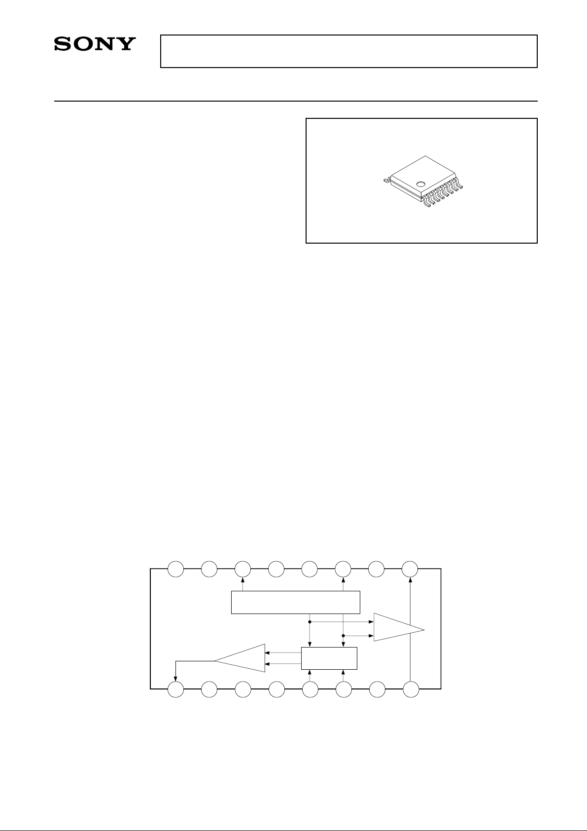
The CXA3068N is a monolithic IC to down-convert
the L-band (930 to 2150 MHz) signal for the satellite
broadcasting receiver. It has a double-balanced
mixer, local oscillator circuit and IF amplifier on chip.
Features
• Balance-type Colpitts oscillator circuit provides a
stable and wide range oscillation.
Oscillation frequency : 2.63 GHz
• Small leak of the local oscillation signal due to the
double-balanced mixer.
• Oscillation frequency drift is small, caused by the
change of impedance at the pre-stage of RF input.
• Local oscillator output circuit for PLL.
• Single 5 V power supply operation.
• Low current consumption. ICC=53 mA (typ.)
• 16-pin SSOP package contributes to reduction in
set size.
Absolute Maximum Ratings (Ta=25 °C)
• Supply voltage VCC –0.3 to +5.5 V
• Storage temperature Tstg –55 to +150 °C
• Allowable power dissipation
Operating Conditions
• Supply voltage VCC 4.75 to 5.3 V
• Ambient temperature Topr –20 to 75 °C
CXA3068N
16 pin SSOP (Plastic)
PD 625 mW
(When mounted on board)
Applications
• Satellite broadcasting tuners for BS, CS, DSS and
DVB. (Frequency conversion to the second IF)
Structure
Bipolar silicon monolithic IC
Block Diagram and Pin Configuration
VCC1
1 2 3 4 5 6 7 8
GND1
OSCB1
IF AMP
NC
OSC
NC
MIX
OSCB2
GND1
10111213141516
BUFF
OSCOUT1
9
IFOUT
Sony reserves the right to change products and specifications without prior notice. This information does not convey any license by
any implication or otherwise under any patents or other right. Application circuits shown, if any, are typical examples illustrating the
operation of the devices. Sony cannot assume responsibility for any problems arising out of the use of these circuits.
VCC2
GND2
GND2
RFIN1
RFIN2
—1—
GND1
OSCOUT2
E95Z07-TE
Page 2
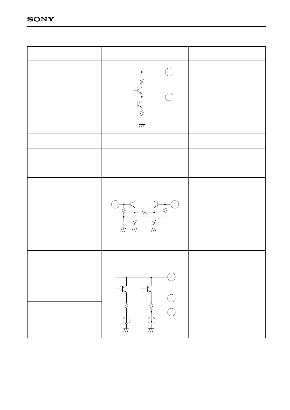
Pin Description and Equivalent Circuit
CXA3068N
Pin
No. voltage (V)
1
2
3
4
Symbol
IF OUT
VCC2
GND2
GND2
Typical pin
2.5
5.0
0
0
Equivalent circuit Description
VCC2
2
1
IF output.
IF block power supply.
IF block GND.
IF block GND.
5
6
7
8
9
RF IN1
RF IN2
GND1
OSC OUT2
OSC OUT1
1.8
1.8
0
3.5
3.5
5 6
2k
40
VCC1
40
2k
16
9
8
RF input.
Normally, a decoupling capacitor
is connected at Pin 5 to GND and
Pin 6 is used for input.
RF block GND.
Local oscillation output.
—2—
Page 3
CXA3068N
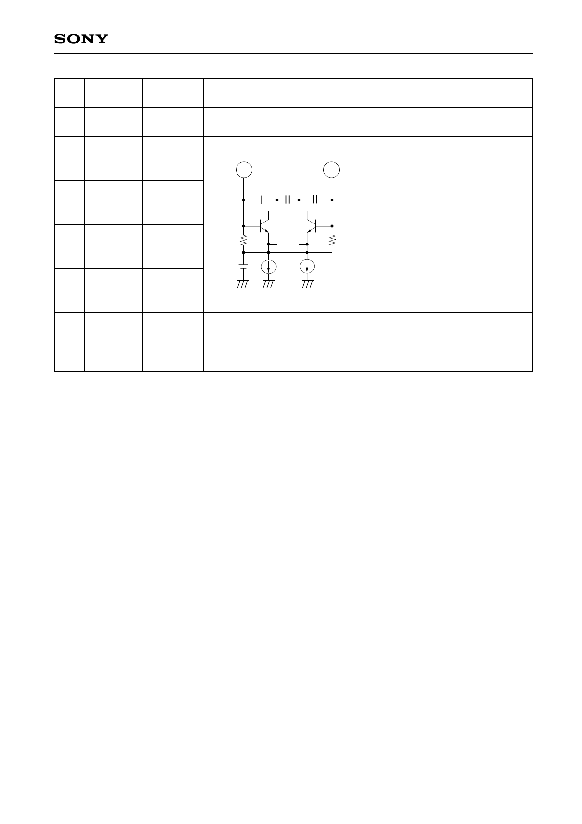
Pin
No. voltage (V)
10
11
12
13
14
15
16
Symbol
GND1
OSC B2
NC
NC
OSC B1
GND1
VCC1
Typical pin
0
2.4
—
—
2.4
0
5.0
Equivalent circuit Description
RF block GND.
14 11
Oscillator.
2k
2k
RF block GND.
RF block power supply.
—3—
Page 4
CXA3068N
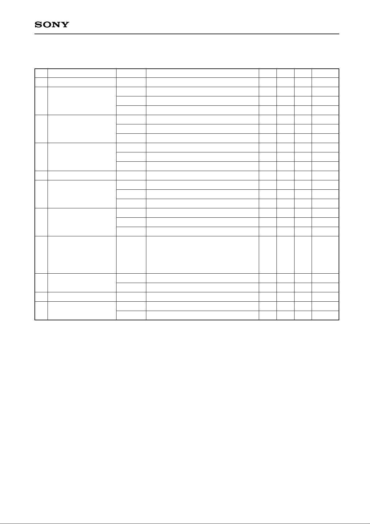
Electrical Characteristics (Ta=25 °C, VCC=5 V, refer to the Electrical Characteristics Measurement Circuit.)
Input frequency: 950 to 2150 MHz
No
1
Current consumption
2
Conversion gain ∗1
3
Noise figure ∗1, 2
4
Local oscillation output
5
IF maximum output
RF pin local oscillation
6
leakage
IF pin local oscillation
7
leakage
Third-order
8
intermodulation
distortion ∗1, 3
Local oscillation phase
9
noise
10
IF output VSWR
11
RF input impedance
∗
1) Measured value for untuned inputs.
∗
2) Noise figure is uncorrected for image.
∗
3) Measure S/I of the desired intermediate frequency (480 MHz) and distortion component (460 MHz) with a
Item
Symbol
ICC
CG1
CG2
CG3
NF1
NF2
NF3
POSC1
POSC2
POSC3
PO (sat)
RFLK1
RFLK2
RFLK3
IFLK1
IFLK2
IFLK3
IM3
CN1
CN2
IFVSWR
rπ
Cπ
Measurement conditions
No signal
fin = 950 MHz, fIF = 480 MHz
fin = 1450 MHz, fIF = 480 MHz
fin = 2150 MHz, fIF = 480 MHz
fin = 950 MHz, fIF = 480 MHz
fin = 1450 MHz, fIF = 480 MHz
fin = 2150 MHz, fIF = 480 MHz
fOSC = 1430 to 1830 MHz
fOSC = 1830 to 2230 MHz
fOSC = 2230 to 2630 MHz
fIF = 480 MHz
fOSC = 1430 to 1830 MHz
fOSC = 1830 to 2230 MHz
fOSC = 2230 to 2630 MHz
fOSC = 1430 to 1830 MHz
fOSC = 1830 to 2230 MHz
fOSC = 2230 to 2630 MHz
Pin = –25 dBm
fin = 950 MHz + 960 MHz
fout = 470 MHz + 480 MHz
S/I of 460 MHz and 480 MHz
fOSC=1430 MHz, offset 10 kHz
fOSC=1430 MHz, offset 100 kHz
f = 480 MHz
f = 950 MHz
Min.
31.0
16
18
19
–10
–10
–11
5.5
Typ.
53.0
19
21
22
16
14
14
–6
–6
–7
8.5
45.0
74
95
1.2
140
5
Max.
75.0
23
25
26
19
16
16
11.0
–20
–20
–20
–20
–32
–32
Unit
mA
dB
dB
dB
dB
dB
dB
dBm
dBm
dBm
dBm
dBm
dBm
dBm
dBm
dBm
dBm
dB
dBc/Hz
dBc/Hz
Ω
pF
spectrum analyzer, assuming input level of the reception frequency to be –25 dBm (when IC input pin is
converted for 50 Ω).
—4—
Page 5

LOout
CXA3068N
1n
20k
1T379
1T379
10k
10k
47p
47p
1013 12 91116 15 14
NC
NC
GND1
OSCB2
OSCB1
GND1
OSCOUT2
CXA3068N
OSCOUT1
GND1
RFIN2
RFIN1
GND2
GND2
VCC2
2 61 87543
1n
100p
RFin
100p
1n
6P
1n
VC
+5V
Electrical Characteristics Measurement Circuit
VCC1
—5—
1n
IF OUT
IFout
Page 6

Description of Operation (Refer to the Electrical Characteristics Measurement Circuit.)
1) Oscillator circuit
The oscillator circuit is formed with two Colpitts oscillators, and oscillation is provided at the differential
input via an LC resonance circuit including a varicap diode. This is oscillated only by attaching an LC
resonance circuit externally because feedback capacitance, etc. are built in for oscillation.
2) Mixer circuit
This is a double-balance mixer having small leak of local oscillation signal. The RF signal is input to Pins
5 and 6. In normal use, the signal is input to one pin while the other pin is connected to GND via
decoupling capacitor.
3) IF amplifier circuit
The mixer output signal is amplified by the IF amplifier and output to Pin 1. The IF output is emitterfollower output and output impedance is approximately 50 Ω (480 MHz).
4) PLL oscillation signal output circuit
The output circuit is built in to drive the PLL for tuning. This is emitter-follower output and output
impedance is approximately 50 Ω.
CXA3068N
—6—
Page 7

CXA3068N
Current consumption vs. Supply voltage
60
55
50
Current consumption [mA]
45
Supply voltage [V]
Conversion gain vs. Reception frequency (untuned input)
25
fIF = 480MHz
20
15
Conversion gain
10
5.35.04.7
0.8 1.2 1.4 1.8 2.2
Reception frequency [GHz]
2.01.61.0
Noise figure vs. Reception frequency (untuned input, in DSB)
24
fIF = 480MHz
20
16
Noise figure [dB]
12
2.01.61.00.8 1.2 1.4 1.8 2.2
Reception frequency [GHz]
Local oscillation output level vs. Local oscillation frequency
+5
0
–5
–10
Local oscillation output level [dBm]
2.62.21.61.4 1.8 2.0 2.4 2.8
Local oscillation frequency [GHz]
—7—
Page 8

CXA3068N
IF pin local oscillation leak vs. Local oscillation frequency
–20
–30
–40
–50
–60
IF pin local oscillation leak [dBm]
1.4 1.6 1.8 2.0 2.2 2.4 2.6 2.8 1.4 1.6 1.8 2.0 2.2 2.4 2.6 2.8
Local oscillation frequency [GHz]
Input/output characteristics (untuned input)
+10
0
RF pin oscillation frequency leak vs. Local oscillation frequency
–20
–30
–40
–50
–60
RF pin oscillation frequency leak [dBm]
Local oscillation frequency [GHz]
= Fundamental-frequency (480MHz)
= Third-harmonics (470MHz)
–10
–20
–30
–50
IF output level [dBm]
–40
–60
–70
–50 –40 –30 –20 –10 0
RF input level [dBm]
(935MHz, 940MHz)
—8—
Page 9

Input Impedance
CXA3068N
j10
0
–j10
1450MHz
j25
–j25
j50
50
2150MHz
–j100
j100
j150
–j150
j250
–j250
5 6
7
8
950MHz
–j50
S11
—9—
Page 10

Output Impedance (IF)
CXA3068N
480MHz
j10
0
–j10
j25
–j25
50
–j50
j50
400MHz
j100
j150
j250
–j250
–j150
2 31
–j100
S11
Output Impedance (local oscillation output)
j50
j25
2630MHz
j10
0
–j10
–j25
50
–j100
j100
j150
–j150
j250
–j250
6 87
1011
9
–j50
1430MHZ
—10—
S11
Page 11

Package Outline Unit : mm
CXA3068N
16PIN SSOP (PLASTIC)
+ 0.1
0.22 – 0.05
16
1
∗5.0 ± 0.1
9
8
0.65 ± 0.12
∗4.4 ± 0.1
0.1 ± 0.1
0.5 ± 0.2
A
+ 0.05
0.15 – 0.02
+ 0.2
1.25 – 0.1
0.1
6.4 ± 0.2
0° to 10°
DETAIL A
NOTE: Dimension “∗” does not include mold protrusion.
SONY CODE
EIAJ CODE
JEDEC CODE
SSOP-16P-L01
SSOP016-P-0044
PACKAGE STRUCTURE
PACKAGE MATERIAL
LEAD TREATMENT
LEAD MATERIAL
PACKAGE WEIGHT
EPOXY RESIN
SOLDER / PALLADIUM
COPPER / 42 ALLOY
0.1g
PLATING
—11—
 Loading...