

Page 1

Decoder/Driver/Timing Generator for Color LCD Panels
Description
The CXA3017R is an IC designed to drive the color
LCD panels LCX005BK/BKB, LCX009AK/AKB,
LCX024AK/AKB, LCX027AK/AKB and DCX501BK.
This IC allows two-panel simultaneous and switching
drive by simultaneously outputting the timing pulses
for the LCX005BK/BKB, LCX009AK/AKB, LCX024AK/AKB,
LCX027AK/AKB and DCX501BK.
This IC greatly reduces the number of peripheral
circuits and parts by incorporating an RGB decoder,
driver, and timing generator for video signals onto a
single chip. This chip has a built-in serial interface
circuit and electronic attenuators which allow various
settings to be performed by microcomputer control,
etc.
Features
• Color LCD panel LCX005BK/BKB, LCX009AK/AKB,
LCX024AK/AKB, LCX027AK/AKB and DCX501BK driver
• Supports two-panel simultaneous and switching
drive using the LCX005BK/BKB, LCX009AK/AKB,
LCX024AK/AKB, LCX027AK/AKB and the DCX501BK
• Supports NTSC and PAL systems
• Supports 16:9 wide display
(letter box and pulse elimination display)
• Supports composite inputs, Y/C inputs and Y/color
difference inputs
• Serial interface circuit
• Electronic attenuators (D/A converter)
• VCO
• BPF, trap and delay line
• Sharpness function
• 2-point γ correction circuit
• R, G, B signal delay time adjustment circuit
• Polarity inversion circuit (line inverted mode)
• Supports external RGB input
• D/A output pin (0 to 3V, 8 levels)
• Supports AC drive for LCD panel during no signal
Applications
• Compact LCD monitors
• LCD viewfinders
• Compact liquid crystal projectors, etc.
Structure
Bi-CMOS IC
Absolute Maximum Ratings (Ta = 25°C)
• Supply voltage VCC1 – GND1 6 V
VCC2 – GND2 14 V
VCC3 – GND3 14 V
VDD1, 2 – VSS 4.5 V
• Analog input pin voltageVINA –0.3 to VCC1V
•Digital input pin voltage VIND –0.3 to VDD1 + 0.3V
• Operating temperature Topr –15 to +75 °C
• Storage temperature Tstg –40 to +125 °C
• Allowable power dissipation
∗1
PD (Ta ≤ 75°C)
Approximately 350mW
Operating Conditions
Supply voltage VCC1 – GND1 2.7 to 3.6 V
VCC2 – GND2 11.0 to 13.5 V
VCC3 – GND3 11.0 to 13.5 V
VDD1, 2 – VSS 2.7 to 3.6 V
∗1
With substrate Size: 30 × 30 × 1.6mm
Material: Glass fabric base epoxy
– 1 –
E98Y29-PS
Sony reserves the right to change products and specifications without prior notice. This information does not convey any license by
any implication or otherwise under any patents or other right. Application circuits shown, if any, are typical examples illustrating the
operation of the devices. Sony cannot assume responsibility for any problems arising out of the use of these circuits.
CXA3017R
64 pin LQFP (Plastic)
For the availability of this product, please contact the sales office.
Page 2

– 2 –
CXA3017R
Block Diagram
SIG.CENTER
POL SW
SUBBRIGHT
GAMMA
DEMOD
LPF
CONTRAST
EXT SW
BRIGHT
S/H
INT/EXT
VXO
HUE
PS
KILLER
FILT ADJ
COLOR CONT
BPF
PIC CONT
DL1
TRAP
CLAMP
ACC AMP
H.FILTER
REG
R G B
+12V
+12V
GND1
V
SS
+3.0V
Buf
EXT COLOR
& BALANCE
HUE
HUE
COLOR
R-BRT
B-BRT
γ -1
γ -2
D/A
VGATE
VJOG
VPAL
VWIN
WIDE
PALSW
D/A
HCNT
H-PULSE
HAFC
PLL-COUNTER
& DECODER
HGATE
H-SKEW DET
PD
CLP
BGP
SBLK
+3V
MATRIX
Buf
POL SW
PSIGBRIGHT
PSIG-BRT
APC
ACC DET
HD
GND3
GND2
FRP
COLOR
PAL ID
CLAMP
DA OUT
VD
EN2
EN1
XEN1
VCK1
VCK2
VCK3
VCK4
VST
XVST
HD
PCG
XPCG
HCK1
HCK2
V
SS
XHST1
HST1
HST2
CLR
BLK
SCLK
DATA
LOAD
V
DD
1
TRAP
EXT B
EXT G
EXT R
TEST1
RPD
VCC1
VXO OUT
VXO IN
APC
R-Y IN
C OUT
V REG
C IN
RESET
Y IN
TEST2
SYNC IN
VSEP TC
GND1
F0 ADJ
B-Y IN
V
DD
2
DWN
RGT1
FB PSIG
GND3
PSIG
V
CC
3
B OUT
FB B
GND2
FB G
R OUT
FB R
V
CC
2
G OUT
BRIGHT
2
3
4
5
6
7
8
9
10
11
12
13
14 15
16
17
18
19
20
21
22
23
24
25
26
27
28
29
30
40
39
38
37
36
35
34
31
32
33
41
42
43
44
45
46
47
48
49
50
51
52
53
54
55
56
57
58
59
60
63
64
61
62
1
Buf
Buf
BLKLIM
WHTLIM
USER
BRIGHT
+3V
I/F
HUE
COLOR
BRIGHT
CONT
R-BRT
B-BRT
γ-1
VCO
PSIG-BRT
R-CONT
B-CONT
PICTURE
USER-BRT
BLKLIM
WHTLIM
γ-2
SERIAL BAS I/F
PALSW
INT/EXT
USERBRT
VCO
VCO
SYNC SEP
V SEP
PICTURE
SUB
CONTRAST
R-CONT
B-CONT
CONT
Page 3

– 3 –
CXA3017R
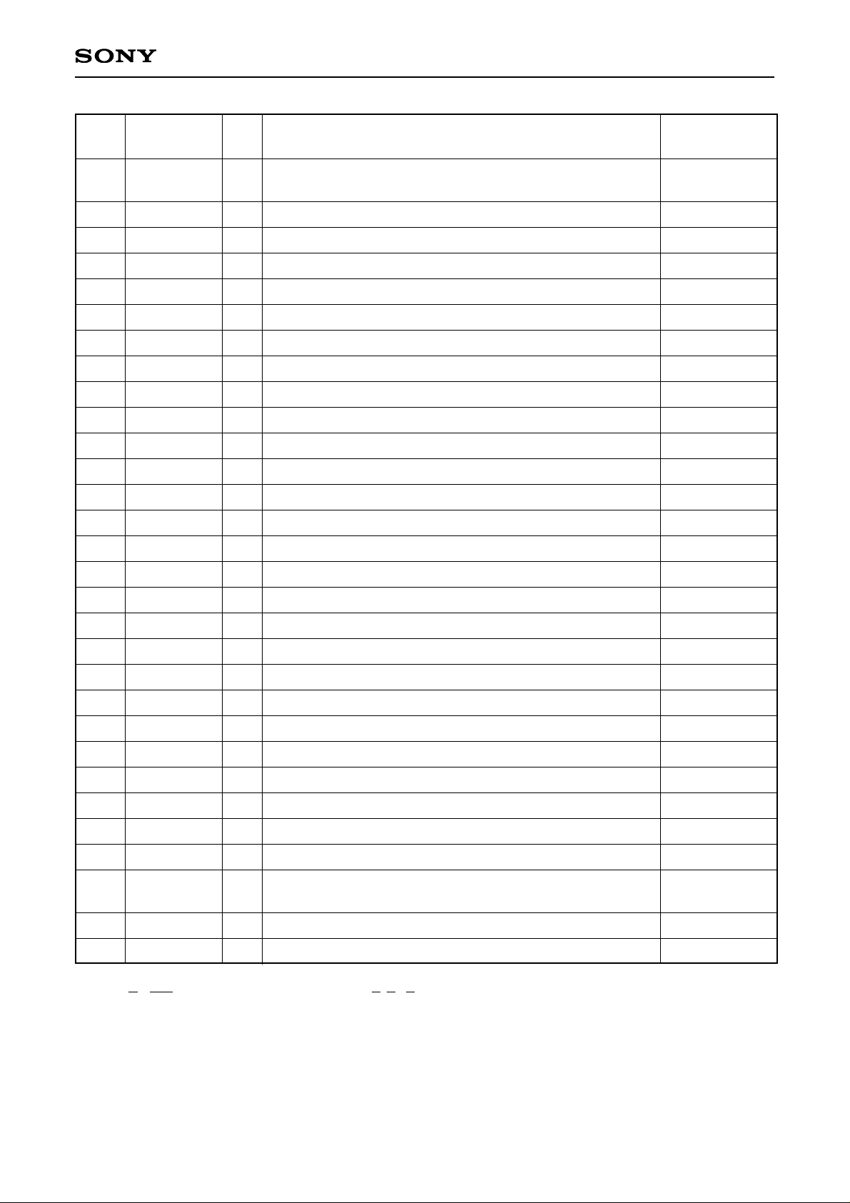
Pin Description
Pin
No.
1
2
3
4
5
6
7
8
9
10
11
12
13
14
15
16
17
18
19
20
21
22
23
24
25
26
27
28
29
30
31
32
33
34
EXT R
EXT G
EXT B
TRAP
VDD1
LOAD
DATA
SCLK
RPD
TEST1
BLK
CLR
HST2
HST1
XHST1
VSS
HCK2
HCK1
XPCG
PCG
HD
XVST
VST
VCK4
VCK3
VCK2
VCK1
XEN1
EN1
EN2
VD
DA OUT
VDD2
DWN
Symbol
L
I
I
I
O
I
I
I
O
I
O
O
O
O
O
O
O
O
O
O
O
O
O
O
O
O
O
O
O
O
O
O
External digital R input
External digital G input
External digital B input
External trap connection
Digital 3V power supply for oscillation cell
Serial interface load input
Serial interface data input
Serial interface clock input
Phase comparator output
Test (Connect to GND.)
BLK pulse output
CLR pulse output
H start pulse 2 output
H start pulse 1 output
XH start pulse 1 output (reverse polarity of HST1)
Digital 3V GND
H clock pulse 2 output
H clock pulse 1 output
XPCG pulse output (reverse polarity of PCG)
PCG (precharge) pulse output
HD pulse output
XV start pulse output (reverse polarity of VST)
V start pulse output
V clock pulse 4 output
V clock pulse 3 output
V clock pulse 2 output
V clock pulse 1 output
XEN pulse 1 output (reverse polarity of EN1)
EN pulse 1 output
EN pulse 2 output
VD pulse output
DAC output
Digital 3V power supply
DCX501BK up/down inverted display switching
(open collector output)
I/O Description
Input pin processing
for open status
Page 4
– 4 –
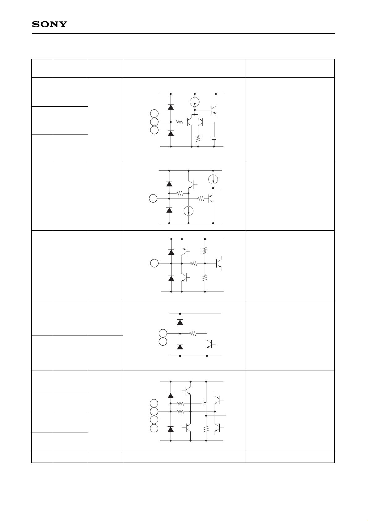
CXA3017R
Pin
No.
35
36
37
38
39
40
41
42
43
44
45
46
47
48
49
50
51
52
53
54
55
56
57
58
59
60
61
62
63
64
L
RGT1
FB PSIG
GND3
PSIG
VCC3
B OUT
FB B
GND2
G OUT
FB G
R OUT
FB R
VCC2
SIG.CENTER
VCC1
VXO OUT
VXO IN
APC
B-Y IN
R-Y IN
C OUT
V REG
C IN
RESET
Y IN
TEST2
SYNC IN
VSEP TC
F0 ADJ
GND1
Symbol
O
I
O
O
I
O
I
O
I
I
O
I
O
I
I
O
O
I
I
I
I
I
O
DCX501BK right/left inverted display switching
(open collector output)
PSIG signal DC voltage feedback circuit capacitor connection
Analog 12V GND for PSIG
PSIG output
Analog 12V power supply for PSIG
B signal output
B signal DC voltage feedback circuit capacitor connection
Analog 12V GND
G signal output
G signal DC voltage feedback circuit capacitor connection
R signal output
R signal DC voltage feedback circuit capacitor connection
Analog 12V power supply
R, G, B and PSIG output DC voltage adjustment
Analog 3V power supply
VXO output
VXO input
APC detective filter connection
B-Y color difference signal input
R-Y color difference signal input
Chroma signal output
Constant voltage capacitor connection
Chroma signal input
System reset
Y signal input
Test (Connect to GND.)
Video input for sync separation
Capacitor connection for vertical sync separation
(or external VSYNC input)
Internal filter adjusting resistor connection
Analog 3V GND
I/O Description
Input pin processing
for open status
∗
DWN: DOWN SCAN and UP SCAN RGT: RIGHT SCAN and LEFT SCAN
Page 5
– 5 –
CXA3017R
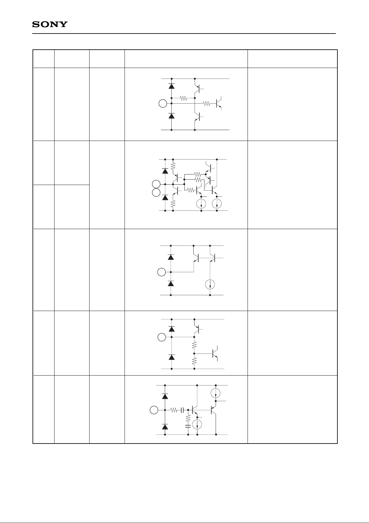
Analog Block Pin Description
Pin
No.
Symbol Pin voltage Equivalent circuit Description
4
TRAP
1.0V
4
VCC1
GND1
200µA
1k
300
75µA
External trap connection.
Connect the trap between this
pin and GND to eliminate the
chroma component.
Leave this pin open when
using Y/C and Y/color
difference mode.
32
DA OUT
0.2 to 2.9V
VDD2
V
SS
50k
50k
32
50k
DAC output.
8-level, 7-step DC voltage from
approximately 0.2 to 2.9V is
output from this pin.
34
35
DWN
—
RGT1
—
35
34
VCC2
GND2
500
DCX501BK up/down and
right/left inversion switching.
These pins are open collector
outputs, so first connect a
100kΩ resistor between these
pins and the panel V
DD (15.5V)
and then connect to the
DCX501BK.
1 EXT-R
2 EXT-G
3 EXT-B
External digital signal inputs.
There are two thresholds: Vth1
(= 1.0V) and Vth2 (= 2.0V).
When one of the RGB signals
exceeds Vth1, all of the RGB
outputs go to black level; when
an input exceeds Vth2, only
the corresponding output goes
to white level.
Connect these pins to GND
when not used.
VCC1
GND1
25µA
300
1.1V
2
3
1
50k
—
41 FB B
36 FB PSIG
44 FB G
46
FB R
Smoothing capacitor
connection for the feedback
circuit of R, G, B and PSIG
output DC level control.
Use a low-leakage capacitor
because of high impedance.
VCC1
GND2
100k
36
41
44
46
1k
1k
1.5V
37 GND3
0V
GND for the PSIG circuit.
Page 6

– 6 –
CXA3017R
48
SIG.
CENTER
VCC2
2
RGB/PSIG output DC voltage
control.
When used with a VCC2 or
VCC3 of 12V or more, or when
used with a signal center
voltage of other than VCC2/2 or
VCC3/2, apply voltage of 5.2 to
6.5V from an external source.
48
VCC2
GND2
150k
300
150k
10k
39
VCC3
12V
12V power supply for the PSIG
circuit.
PSIG signal output.
VCC3
GND3
20
38
150
38
PSIG
VCC2
2
40
B OUT
43
G OUT
45
R OUT
VCC2
2
RGB signal outputs.
VCC2
GND2
40µA
20
20
40
43
45
42
GND2
0V
12V GND.
49 VCC1
3.0V
3.0V power supply.
47 VCC2
12V
12V power supply.
50
VXO OUT
1.2V
VXO output.
Leave this pin open when
using Y/color difference mode.
50
VCC1
GND1
200
370µA
51
VXO IN
1.6V
VXO input.
Leave this pin open when
using Y/color difference mode.
GND1
10k
1.6V
VCC1
500
51
3.5k
10p
3.5k
Pin
No.
Symbol Pin voltage Equivalent circuit Description
Page 7
– 7 –
CXA3017R
Pin
No.
Symbol Pin voltage Equivalent circuit Description
53 B-Y IN
54 R-Y IN
—
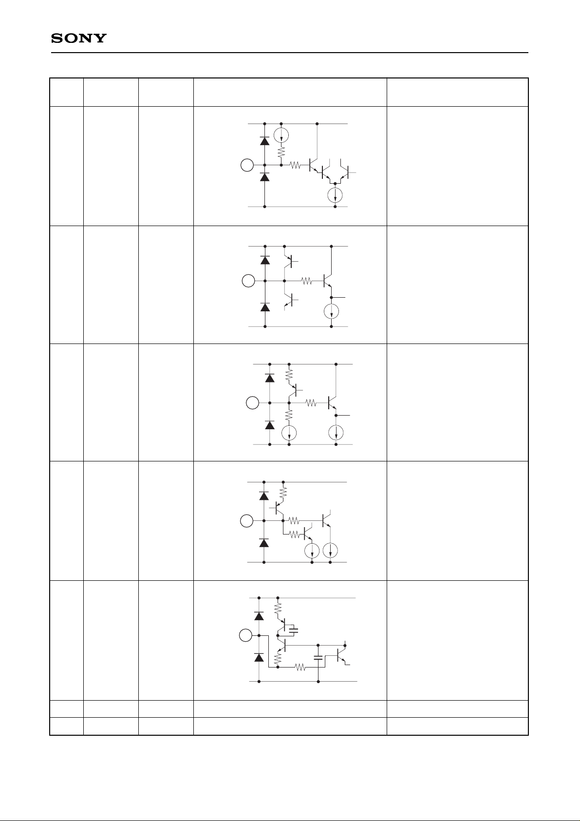
Y/color difference signal inputs.
When using color difference
input, the standard signal input
level is 0.3Vp-p (75% color bar)
and the clamp level is
approximately 1.7V.
During D-PAL, the COUT (Pin
55) chroma signal is U/V
separated and then input.
Input at low impedance (75Ω or
less).
53
54
VCC1
GND1
40µA
4k
4k
10k
5k
1k
30µA
55
C OUT
1.2V
Color adjusted chroma signal
output during D-PAL. The
output level is tripled in order
to compensate for the
attenuation of the external U/V
separation delay line. The
standard burst output level is
approximately 200mVp-p.
Leave this pin open in modes
other than D-PAL.
50µA
VCC1
GND1
55
∗
D-PAL is a demodulation method that uses an external delay line during demodulation.
S-PAL is a demodulation method that internally processes chroma demodulation.
52 APC
1.7V
APC detective filter
connection.
Leave this pin open when
using Y/color difference mode.
1k
GND1
VCC1
52
500
56 V REG
2.0V
Smoothing capacitor
connection for the internally
generated constant voltage
source circuit.
Connect a capacitor of 1µF or
more.
VCC1
GND1
18.5k
30k
56
57
C IN —
Video signal input when using
composite signal input.
Chroma signal input when
using Y/C signal input.
Leave this pin open when
using Y/color difference mode.
57
50k
V
CC1
GND1
15µA
50k
5p
10p
30µA
Page 8
– 8 –
CXA3017R
Pin
No.
Symbol Pin voltage Equivalent circuit Description
58
RESET
—
TG block system reset pin.
The system is reset when this
pin is connected to GND.
Connect a capacitor between
this pin and GND.
1k
V
DD1
GND1
2µA
58
300
59
Y IN
Y signal input.
The standard signal input level
is 0.5Vp-p (100% white level
from the sync tip).
Input at low impedance (75Ω
or less).
VCC1
GND1
59
20µA
1k
63
F0 ADJ
1.5V
Filter reference current
generation.
Connect resistance of 15 kΩ
between this pin and GND1 to
adjust the internal filters using
the outflow current value.
Leave this pin open when
using Y/C or Y/color difference
mode.
VCC1
GND1
200
500
5p
63
500
5p
62
VSEP TC
1.7V
Capacitor connection for
vertical sync separation.
VDD1
GND1
20µA
20µA
500
1k
62
1k
1.6V
61 SYNC IN
1.6V
Sync input.
Normally inputs the Y signal.
The standard signal input level
is 0.5Vp-p (100% white level
from the sync tip).
Input at low impedance (75Ω
or less).
VDD1
GND1
12µA
1k
61
0.6µA
500
1k
64 GND1
0V
3.0V GND.
60
TEST2
0V
Test. Connect to GND.
Page 9
– 9 –
CXA3017R
Pin
No.
Symbol Pin voltage Equivalent circuit Description
Digital Block Pin Description
VSS
1k
6
7
8
5 VDD1
6 LOAD
7 DATA
8 SCLK
9
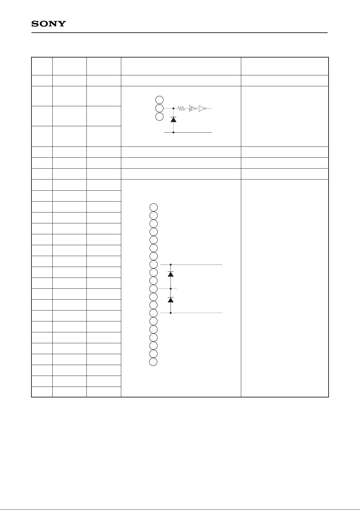
33
10
RPD
VDD2
TEST1
Power supply for VCO.
Serial bus inputs.
Phase comparator output.
Power supply for digital block.
Test. Connect to GND.
VDD2
V
SS
11
12
13
14
15
17
18
19
20
21
22
23
24
25
26
27
28
29
30
31
11
12
13
14
15
17
18
19
20
21
22
23
24
25
26
27
28
29
30
31
BLK
CLR
HST2
HST1
XHST1
HCK2
HCK1
XPCG
PCG
HD
XVST
VST
VCK4
VCK3
VCK2
VCK1
XEN1
EN1
EN2
VD
Digital block outputs.
Page 10

– 10 –
CXA3017R
Setting Conditions for Measuring Electrical Characteristics
Use the Electrical Characteristics Measurement Circuit on page 30 while measuring electrical characteristics.
Also, the TG (timing generator) block must be initialized by performing Settings 1 and 2 below.
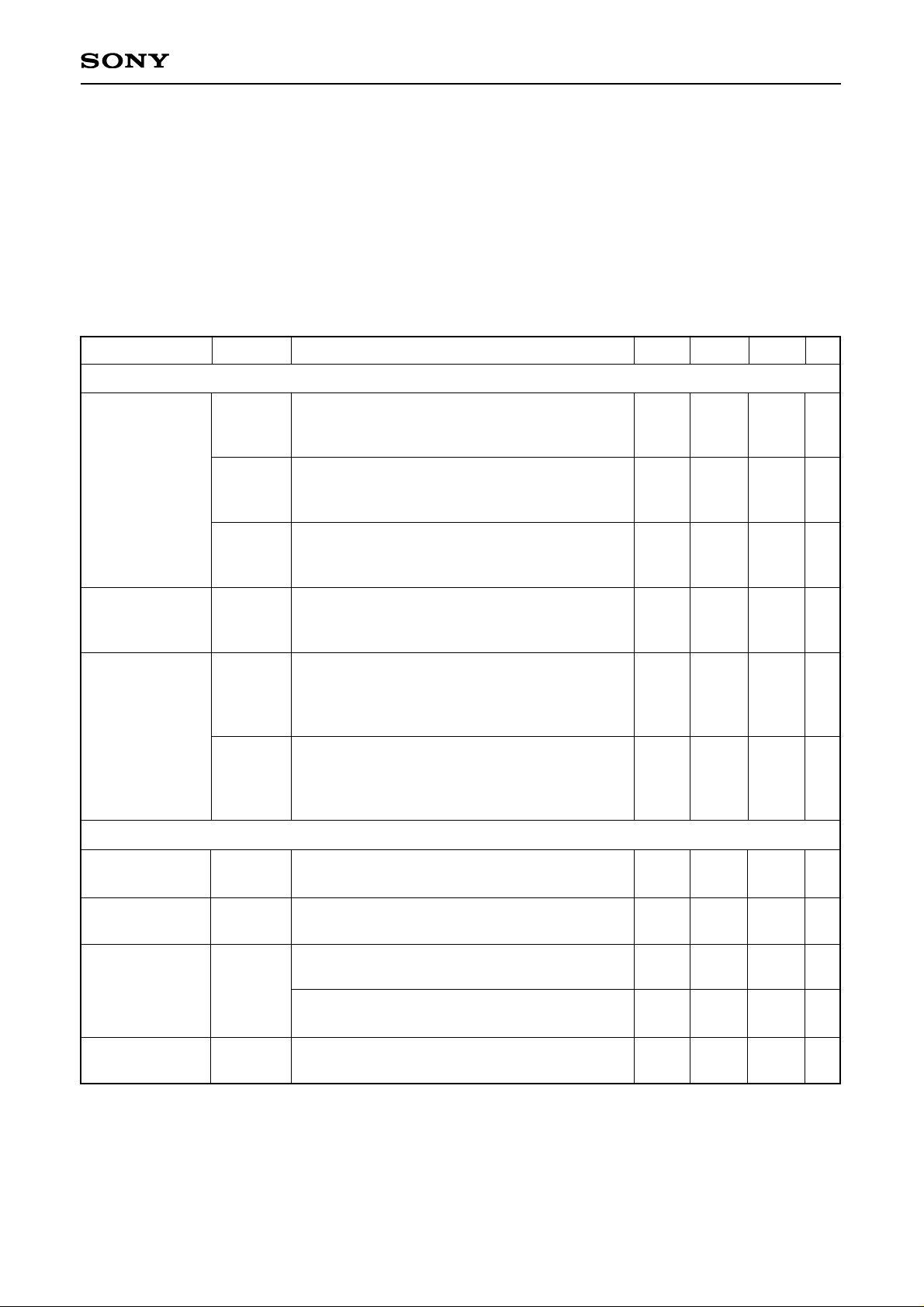
Setting 1. System reset
After turning on the power, set SW58 to ON and start up V58 from GND in order to activate the TG
block system reset. (See Fig. 1-1.)
The serial bus is set to the default values.
Setting 2. Horizontal AFC adjustment
Input SIG5 (VL = 0mV) to (A) and adjust serial bus register VCO so that the TP9 phase comparison
output waveform (near VSYNC) is horizontal.
SW48 = OFF, SW58 = ON, V58 = 3.0V
(See Fig. 1-2.)
Note) When measuring a band of 2MHz or more such as Y signal frequency response or sharpness characteristics
among the items being measured, the measurement must be made with the sample-and-hold circuit set to
through (sample and hold not performed) by the serial bus.
VDD
TR
TR > 10µs
V58 (PWRST)
SIG5
TP9
TP9
approximately 1/2V
DD
VSYNC VSYNC
Adjust to a horizontal waveform.
Fig. 1-1. System reset
Fig. 1-2. Horizontal AFC adjustment
Page 11
– 11 –
CXA3017R
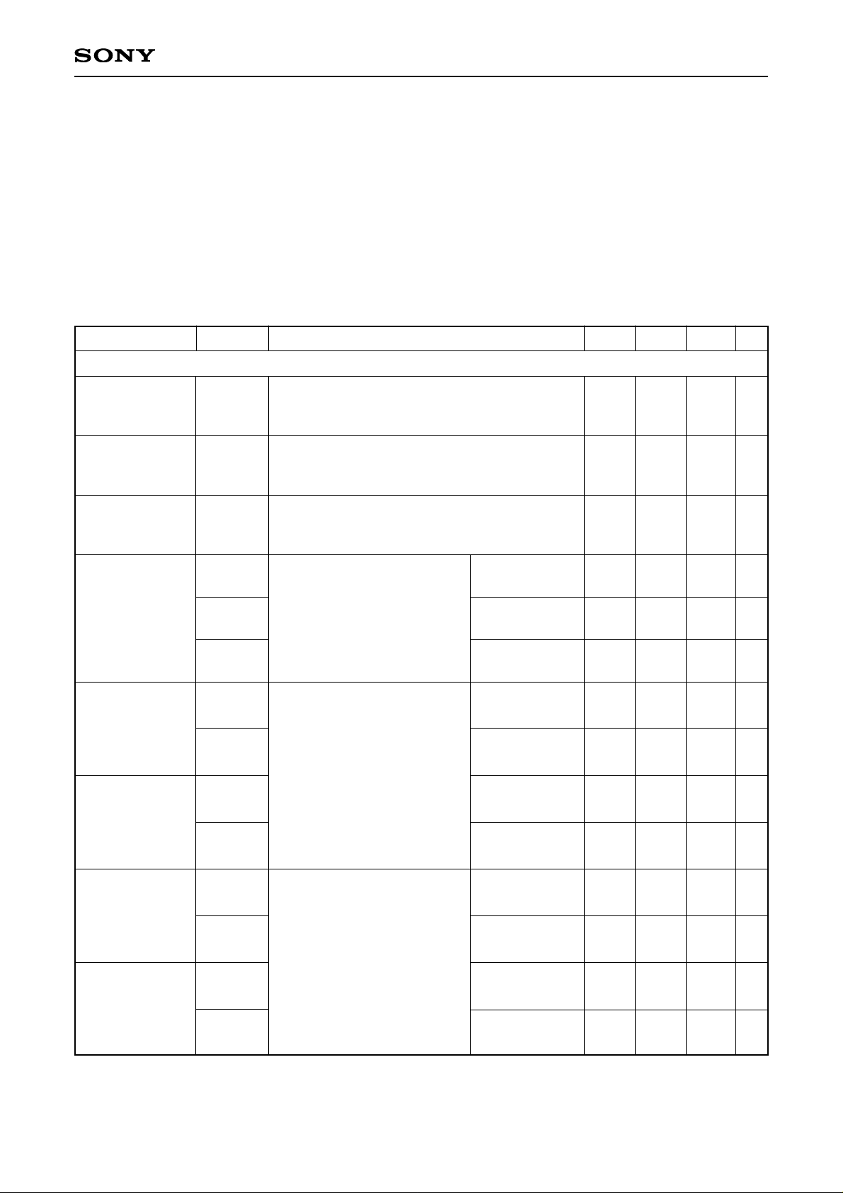
Digital block I/O characteristics
Digital block input pins
∗
1
SW57 = A (A) = SIG4, (B) = SIG2
0.3V
DD
V
VIL
Low level input
voltage
Digital block input pins
∗
1
SW57 = A (A) = SIG4, (B) = SIG2
0.7V
DD
V
VIH
High level input
voltage
VDD = 3.0V IOH = –1.2mA
∗
2
SW57 = A (A) = SIG4, (B) = SIG2
2.8
V
VOH1
High level output
voltage
VDD = 2.7V IOH = –1.2mA
∗
2
SW57 = A (A) = SIG4, (B) = SIG2
2.6
V
IOL = 1.2mA
∗
2
SW57 = A (A) = SIG4, (B) = SIG2
0.3
V
VOL1
Low level output
voltage
∗1
Digital block input pins: SCLK, DATA, LOAD
∗2
Output pins except RPD: BLK, CLR, HST2, HST1, XHST1, HCK2, HCK1, XPCG, PCG, HD, XVST, VST,
VCK4, VCK3, VCK2, VCK1, XEN1, EN1, EN2, VD
Electrical Characteristics — DC Characteristics
Unless otherwise specified, Settings 1 and 2 and the following setting conditions are required.
VCC1 = 3.0V, VCC2 = VCC3 = 12.0V, GND1 = GND2 = GND3 = 0V, VDD1 = VDD2 = 3.0V, VSS = 0V, Ta = 25°C
SW1/SW2/SW3 = A, SW53/SW54/SW57 = B
SW58 = ON, SW48 = OFF
V58 = 3.0V
Set the serial bus registers to the "Serial Bus Register Initial Settings". Unspecified items should be set to the
default settings.
Input SIG4 to (A) and SIG2 (0dB) to (B), and measure
the I
CC1 current value. COMP input mode.
SW57 = A
Input SIG4 to (A) and SIG2 (0dB) to (B), and measure
the I
CC1 current value. Y/C input mode.
SW57 = A
Input SIG4 to (A), (D) and (E) and measure the I
CC1
current value. Y/color difference input mode.
SW53 = SW54 = A
Input SIG4 to (A) and SIG2 (0dB) to (B), and measure
the I
CC2 current value.
SW57 = A
Input SIG4 to (A) and SIG2 (0dB) to (B), and measure
the I
DD3 and IDD4 current values.
I
DD1 = IDD3 + IDD4, LCX009AK/AKB
SW57 = A
Input SIG4 to (A) and SIG2 (0dB) to (B), and measure
the I
DD3 and IDD4 current values.
I
DD2 = IDD3 + IDD4, LCX005BK/BKB
SW57 = A
27
24
19
6
8.5
7.5
34
30
25
8
11
10
41
37
30
10
13.5
12.5
mA
mA
mA
mA
mA
mA
I
CC11
I
CC12
I
CC13
I
CC2
I
DD1
IDD2
Item
Current characteristics
Current
consumption
VCC1
Current
consumption
V
CC2, 3
Current
consumption
V
DD1, 2
Symbol Conditions Min. Typ. Max. Unit
Page 12
– 12 –
CXA3017R
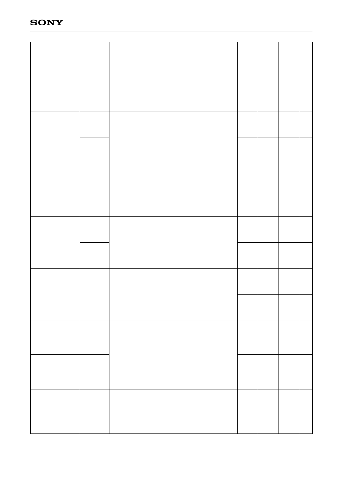
Electrical Characteristics — AC Characteristics
Unless otherwise specified, Settings 1 and 2 and the following setting conditions are required.
VCC1 = 3.0V, VCC2 = VCC3 = 12.0V, GND1 = GND2 = GND3 = 0V, VDD1 = VDD2 = 3.0V, VSS = 0V, Ta = 25°C
SW1, SW2, SW3 = A SW53, SW54, SW57 = B
SW58 = ON SW48 = OFF
V58 = 3.0V
Set the serial bus registers to the "Serial Bus Register Initial Settings". Unspecified items should be set to the
default settings.
Unless otherwise specified, measure the non-inverted outputs for TP40, TP43 and TP45.
19
14
–3
5.0
2.5
3.0
21
16
1
23
18
3
dB
dB
dB
MHz
MHz
MHz
GV
GCNTTP
GCNTMN
FCYYC
FCYCMN
FCYCMP
Item
Y signal system
Video maximum
gain
Contrast
characteristics
TYP
Contrast
characteristics
MIN
Y signal frequency
response
11 14
–3 0
11 14
–1
2
dB
dB
dB
dB
8
11
dB
–5
–2
dB
6
9
dB
–6
–3
dB
GSHP1X
GSHP1N
GSHP2X
GSHP2N
Picture quality
adjustment
variable amount 1
(Y/C input)
LCX009AK/AKB
Picture quality
adjustment
variable amount 2
(Y/C input)
LCX005BK/BKB
Symbol Conditions Min. Typ. Max. Unit
Y/C input
Composite input
(NTSC)
Composite input
(PAL)
2.5MHz MAX
2.5MHz MIN
1.8MHz MAX
1.8MHz MIN
1.8MHz MAX
1.8MHz MIN
2.5MHz MAX
2.5MHz MIN
Input SIG4 to (A) and measure the ratio between the
output amplitude (white-black) and input amplitude at
TP43.
Input SIG4 to (A) and measure the ratio between the
output amplitude (white-black) and input amplitude at
TP43.
Input SIG4 to (A) and measure the ratio between the
output amplitude (white-black) and input amplitude at
TP43.
Assume the output amplitude at
TP43 when SIG1 (0dB, no burst,
100kHz) is input to (A) as 0dB.
Vary the frequency of the input
signal to obtain the frequency
with an output amplitude of –3dB.
CL = 400pF
Assume the output amplitude at
TP43 when SIG7 (100kHz) is
input to (A) as 0dB. Obtain the
amount by which the output
amplitude of SIG7 (2.5MHz or
1.8MHz) changes when PICTURE
is set to the MAX and MIN values.
GSHP3X
GSHP3N
GSHP4X
GSHP4N
Picture quality
adjustment
variable amount 3
(composite input)
LCX005BK/BKB
Picture quality
adjustment
variable amount 4
(composite input)
LCX009AK/AKB
Assume the output amplitude at
TP43 when SIG7 (100kHz) is
input to (A) as 0dB. Obtain the
amount by which the output
amplitude of SIG7 (1.8MHz or
2.5MHz) changes when PICTURE
is set to the MAX and MIN values.
Page 13

– 13 –
CXA3017R
Input SIG2 (0dB) to (A). Using a spectrum analyzer,
measure the input and the 3.58MHz or 4.43MHz
component of TP43, and obtain
CRLEKY = 150mV × 10
∆CLK/20
using their difference ∆CLK.
CRLEKY 30 mV
Carrier leak
(residual carrier)
TDYYC
TDYCMN
TDYCMP
TDYDEF
260
520
520
100
360
620
620
200
460
720
720
300
ns
ns
ns
ns
Y signal I/O delay
time
Y/C input
Composite input
(NTSC)
Composite input
(PAL)
Y/color difference input
SW53 = SW54 = A
Input SIG9 to (A). Measure
the delay time from the 2T
pulse peak of the input signal
to the 2T pulse peak of the
non-inverted output at TP43.
–3
0
3 dB
–3 0 3
dB
–3
0
3
dB
–3
±500
Hz
±500 Hz
+3 +5 dB
–25
–20
dB
0
3
dB
ACC1
ACC2
FAPC
GCOLMX
GCOLMN
Item
Chroma signal block
ACC amplitude
characteristics 1
ACC amplitude
characteristics 2
APC pull-in range
Color adjustment
characteristics
MAX
Color adjustment
characteristics
MIN
–30 –40 deg
30 60 deg
HUEMX
HUEMN
HUE adjustment
characteristics
MAX
HUE adjustment
characteristics
MIN
Symbol Conditions Min. Typ. Max. Unit
NTSC
PAL
NTSC
PAL
NTSC
PAL
Input SIG5 (VL = 150mV) to (A) and SIG2
(0dB/+6dB/–20dB, 3.58MHz burst/chroma
phase = 180°, or 4.43MHz burst/chroma
phase = ±135°) to (B). Measure the output
amplitude at TP55, assuming the output
corresponding to 0dB, +6dB and –20dB as
V0, V1 and V2, respectively.
ACC1 = 20 log (V1/V0)
ACC2 = 20 log (V2/V0)
Input SIG5 (VL = 150mV) to (A) and SIG2
(0dB, 3.58MHz burst/chroma phase = 180°,
or 4.43MHz burst/chroma phase = ±135°) to
(B). Vary the SIG2 burst frequency and
measure the frequency f1 at which the TP40
output appears (the killer mode is canceled).
NTSC: FAPCN = f1 – 3579545Hz
PAL: FAPCP = f1 – 4433619Hz
Input SIG5 (VL = 150mV) to (A) and SIG2 (0dB,
3.58MHz burst/chroma phase = 180°) to (B). Assume
the chroma signal amplitude at TP55 when serial bus
register COLOR = 128, 255 and 0 as V0, V1 and V2,
respectively.
GCOLMX = 20 log (V1/V0)
GCOLMN = 20 log (V2/V0)
Input SIG5 (VL = 150mV) to (A) and SIG2 (0dB,
burst/chroma phase variable) to (B). Assume the
phase at which the output amplitude at TP40 reaches
a minimum when serial bus register HUE = 128, 255
and 0 as θ0, θ1 and θ2, respectively.
HUEMX = θ1 – θ0
HUEMN = θ2 – θ0
SW57 = A
Page 14
– 14 –
CXA3017R
Item Symbol Conditions Min. Typ. Max. Unit
θRBN
θGBN
VRBP
VGBP
99
230
109
242
119
254
deg
0.33
0.65
0.40
0.75
0.47
0.85
deg
θRBP
θGBP
80
23290244
100
256
deg
deg
GEXCMX
+3
+5
dB
GEXCMN
Color difference
input color
adjustment
characteristics MAX
Demodulation
output phase
difference (PAL)
Demodulation
output amplitude
ratio (PAL)
Demodulation
output phase
difference (NTSC)
Color difference
input color
adjustment
characteristics MIN
Color difference
balance
–20 –15 dB
VEXCBL 0.8 1.0 1.2
Input SIG5 (VL = 150mV) to (A) and SIG2 (0dB,
3.58MHz) to (B) and vary the chroma phase. Assume
the phase at which the amplitude at TP40, TP43 and
TP45 reaches a maximum as θB, θG and θR,
respectively.
θRBN = θR – θB, θGBN = θG – θB
SW57 = A
Input SIG5 (VL = 150mV) to (A) and SIG2 (0dB,
4.43MHz) to (B) and vary the chroma phase. Assume
the maximum amplitude at TP40 as VB, the maximum
amplitude at TP43 as VG, and the maximum amplitude
at TP45 as VR.
VRBP = VR/VB, VGBP = VG/VB
SW57 = A
Input SIG5 (VL = 150mV) to (A) and SIG2 (0dB,
4.43MHz) to (B) and vary the chroma phase. Assume
the phase at which the amplitude at TP40, TP43 and
TP45 reaches a maximum as θB, θG and θR,
respectively.
θRBP = θR – θB, θGBP = θG – θB
SW57 = A
Input SIG5 (VL = 150mV) to (A) and SIG1 (0dB,
100kHz, no burst) to (D). Assume the output
amplitude at TP40 (100kHz) when serial bus register
COLOR = 128 as VC0, when COLOR = 0 as VC2,
and when SIG1 is set to –10dB and COLOR = 255
as VC1.
GEXCMX = 20 log (VC1/VC0) + 10
GEXCMN = 20 log (VC2/VC0)
SW53 = SW54 = A
Input SIG5 (VL = 150mV) to (A) and SIG1 (0dB,
100kHz, no burst) to (D) and (E). Assume the output
amplitude at TP40 (100kHz) as VB and the output
amplitude at TP45 (100kHz) as VR.
VEXCBL = VR/VB
SW53 = SW54 = A
Input SIG5 (VL = 150mV) to (A) and SIG2
(level variable, 3.58MHz burst/chroma phase
= 180°, or 4.43MHz burst/chroma phase =
±135°) to (B), and measure the output
amplitude at TP40. Gradually reduce the
SIG2 amplitude level and measure the level
at which the killer operation is activated.
SW57 = A
–36 –30 dB
–36
–30
dB
ACKN
ACKP
Killer operation
input level
NTSC
PAL
VGBN
VRBN
0.25
0.53
0.32
0.63
0.39
0.73
Input SIG5 (VL = 150mV) to (A) and SIG2 (0dB,
3.58MHz) to (B) and vary the chroma phase. Assume
the maximum amplitude at TP40 as VB, the maximum
amplitude at TP43 as VG, and the maximum amplitude
at TP45 as VR.
VRBN = VR/VB, VGBN = VG/VB
SW57 = A
Demodulation
output amplitude
ratio (NTSC)
Page 15

– 15 –
CXA3017R
Color difference
input balance
adjustment R
Color difference
input balance
adjustment B
GEXRMX
–5
–2
dB
GEXRMN
+2
+3
dB
GEXBMX
+2
+3 dB
GEXBMN –5 –2
dB
Input SIG5 (VL = 150mV) to (A) and SIG1 (–6dB,
100kHz, no burst) to (D) and (E). Assume the output
amplitude at TP45 (100kHz) and TP40 (100kHz)
when serial bus register HUE = 128 as VR0 and VB0,
respectively, when HUE = 255 as VR1 and VB1,
respectively, and when HUE = 0 as VR2 and VB2,
respectively.
GEXRMX = 20 log (VR1/VR0)
GEXRMN = 20 log (VR2/VR0)
GEXBMX = 20 log (VB1/VB0)
GEXBMN = 20 log (VB2/VB0)
SW53 = SW54 = A
Item Symbol Conditions Min. Typ. Max. Unit
VEXGBN 0.23 0.26 0.29
0.46 0.51 0.56
VEXGRN
5.85
5.2
6.00
0
6.15
100
6.5
V
mV
V
G-Y matrix
characteristics
(NTSC)
Input SIG5 (VL = 150mV) to (A) and SIG1 (0dB,
100kHz, no burst) to (D). Assume the output
amplitude at TP40 (100kHz) as VEXB and the output
amplitude at TP43 (100kHz) as VEXBG.
VEXGBN = VEXBG/VEXB
SW53 = SW54 = A
Input SIG5 (VL = 150mV) to (A) and SIG1 (0dB,
100kHz, no burst) to (E). Assume the output
amplitude at TP45 (100kHz) as VEXR and the output
amplitude at TP43 (100kHz) as VEXRG.
VEXGRN = VEXRG/VEXR
SW53 = SW54 = A
VEXGBP 0.17 0.20 0.23
0.46 0.51 0.56
VEXGRP
G-Y matrix
characteristics
(PAL)
Input SIG5 (VL = 150mV) to (A) and SIG1 (0dB,
100kHz, no burst) to (D). Assume the output
amplitude at TP40 (100kHz) as VEXB and the output
amplitude at TP43 (100kHz) as VEXBG.
VEXGBP = VEXBG/VEXB
SW53 = SW54 = A
Input SIG5 (VL = 150mV) to (A) and SIG1 (0dB,
100kHz, no burst) to (E). Assume the output
amplitude at TP45 (100kHz) as VEXR and the output
amplitude at TP43 (100kHz) as VEXRG.
VEXGRP = VEXRG/VEXR
SW53 = SW54 = A
VOUT
∆VOUT
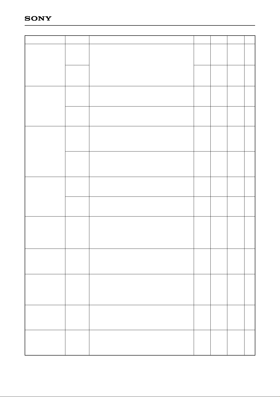
Input SIG5 (VL = 0mV) to (A). Adjust serial bus
registers BRIGHT and PSIG-BRT so that the output
(black-black) at TP43 and TP38 is 9Vp-p and measure
the DC voltage at TP40, TP43, TP45 and TP38.
Input SIG5 (VL = 0mV) to (A). Adjust serial bus
registers BRIGHT and PSIG-BRT so that the output
(black-black) at TP43 and TP38 is 9Vp-p, measure the
DC voltage at TP40, TP43, TP45 and TP38, and obtain
the maximum difference between each of these values.
RGB signal output block
RGB signal and
PSIG output DC
voltage
RGB signal and
PSIG output DC
voltage difference
VORNG
Set V48 to 5.2V or 6.5V in the VOUT measurement
conditions and confirm that ∆VOUT in the preceding
item is satisfied and that |V48 – VOUT| ≤ 0.15V.
SW48 = ON
SIG center variable
range
Page 16
– 16 –
CXA3017R
Item Symbol Conditions Min. Typ. Max. Unit
±1.3
±1.7
V
–3.0
–2.5
V
2.5
3.0
V
SBBRT
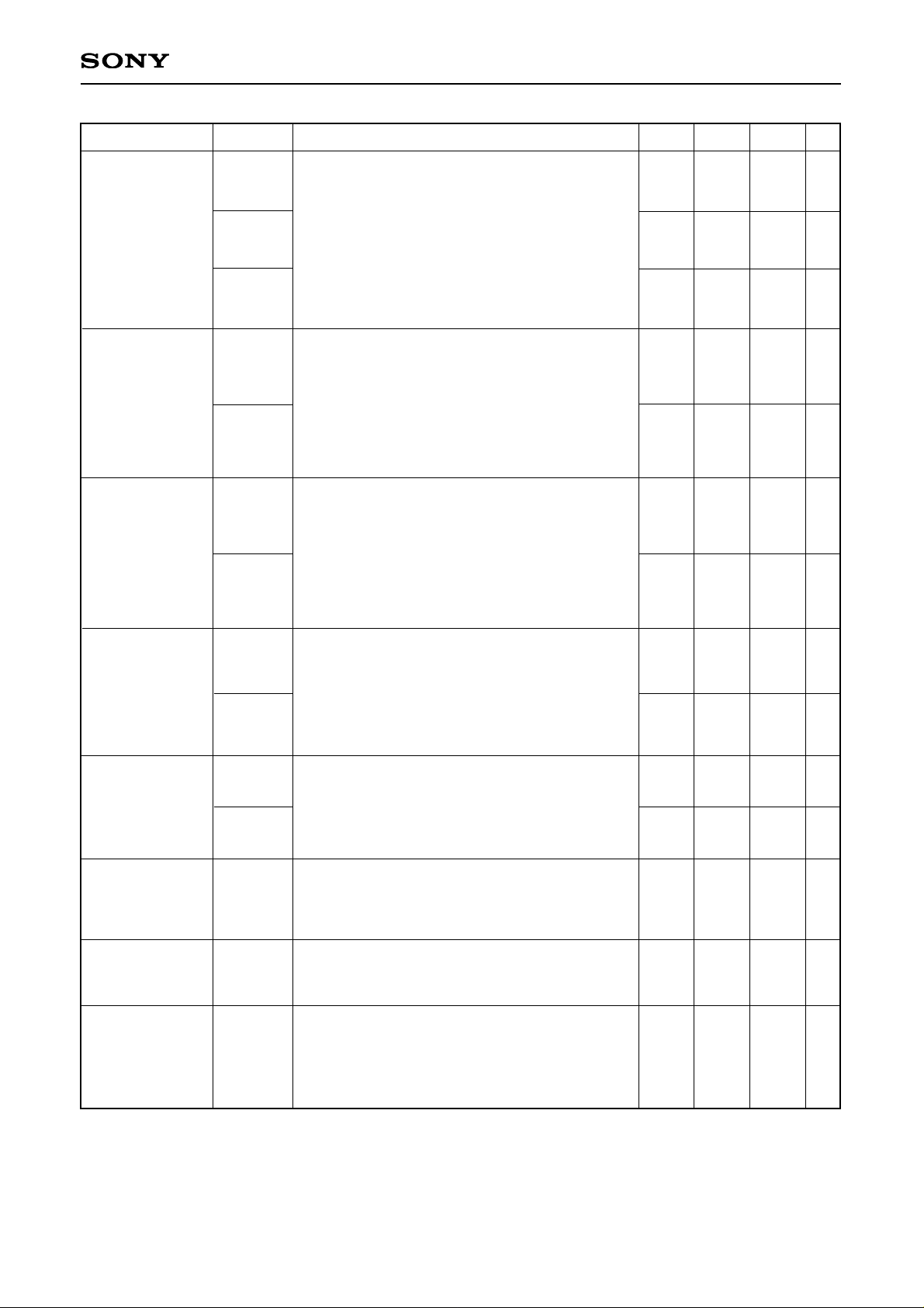
Input SIG5 (VL = 0mV) to (A) and measure the
difference between the outputs (black-black) at TP40
and TP45 and the output (black-black) at TP43 when
serial bus registers R-BRT = B-BRT = 0 and when
R-BRT = B-BRT = 255.
Amount of change
in sub-brightness
–0.6
0
0.6
dB
∆GRGB
Input SIG4 to (A) and obtain the level difference
between the maximum and minimum non-inverted
output amplitudes (white-black) at TP40, TP43 and
TP45.
Difference in gain
between RGB
output signals
±1.5
±2
dB
SBCNT
Input SIG4 to (A) and measure the difference between
the non-inverted outputs (white-black) at TP40 and
TP45 and the non-inverted output (white-black) at
TP43 when serial bus registers R-CNT = B-CNT = 0
and when R-CNT = B-CNT = 255.
Amount of change
in sub-contrast
–0.3
0
0.3
dB
∆GINV
Input SIG4 to (A) and obtain the difference between
the non-inverted output amplitudes (white-black) and
the inverted output amplitudes at TP40, TP43 and
TP45.
Difference in RGB
output inverted/
non-inverted gain
300 mV
∆VBL
Input SIG4 to (A) and obtain the level difference
between the maximum and minimum black levels of
both the inverted and non-inverted outputs at TP40,
TP43 and TP45.
Difference in black
level potential
between RGB
output signals
UBRTMX
UBRTMN
Input SIG3 to (A) and measure the amount of change
in the black level output at TP40, TP43 and TP45
when serial bus register USER-BRT is changed from
128 to 255.
Input SIG3 to (A) and measure the amount of change
in the white level output at TP40, TP43 and TP45
when serial bus register USER-BRT is changed from
128 to 0.
Amount of change
in user brightness
–2.5
–2.0 V
2.0
2.5
V
BRTMX
BRTMN
Input SIG3 to (A) and measure the black level output
at TP40, TP43 and TP45 when serial bus register
BRIGHT is changed from 128 to 255.
Input SIG3 to (A) and measure the white level output
at TP40, TP43 and TP45 when serial bus register
BRIGHT is changed from 128 to 0.
Amount of change
in brightness
PSIGMX
PSIGMN
Input SIG3 (VL = 0mV) to (A) and measure the output
(black-black) at TP38 when serial bus register
PSIG-BRT = 255.
Input SIG3 (VL = 0mV) to (A) and measure the output
(black-black) at TP38 when serial bus register
PSIG-BRT = 0.
Amount of change
in PSIG output
VLIMMX
VLIMMN
Input SIG3 to (A). Vary BLKLIM and measure the
maximum value VLIMMX and minimum value
VLIMMN of the voltage range (black-black) over
which the black limiter operates for the TP38, TP40,
TP43 and TP45 outputs. Assume the value when
BLKLIM = 0 as VLIMMX, and when BLKLIM = 255 as
VLIMMN.
RGB and PSIG
output black limiter
operation voltage
9.0
9.0
7.0
1.5
Vp-p
Vp-p
Vp-p
Vp-p
Page 17
– 17 –
CXA3017R
Input SIG8 to (A). Adjust the non-inverted output
amplitude (black-white) at TP43 to 3.5Vp-p with serial
bus register CONT and the black level at TP43 to 1.5V
with serial bus register RBT.
Measure VG1, VG2 and VG3.
Gγ1 = 20 log (VG1/0.0375)
Gγ2 = 20 log (VG2/0.0375)
Gγ3 = 20 log (VG3/0.0375)
(See Fig. 5 for definitions of VG1, VG2 and VG3.)
Input SIG8 to (A) and adjust serial bus register
BRIGHT so that the output at TP43 is 9Vp-p (blackblack).
Read the point where the gain of the non-inverted
output at TP43 changes when serial bus register
γ1 = 0 and 255 from the input signal IRE level.
Vγ1MN when γ1 = 0, and Vγ 1MX when γ1 = 255.
Input SIG8 to (A) and adjust serial bus register
BRIGHT so that the output at TP43 is 9Vp-p (blackblack).
Read the point where the gain of the non-inverted
output at TP43 changes when serial bus register
γ2 = 0 and 255 from the input signal IRE level.
Vγ2MN when γ2 = 0, and Vγ 2MX when γ2 = 255.
γ gain
γ1 adjustment
variable range
γ2 adjustment
variable range
Gγ1
Gγ2
Gγ3
23.0
26.0
29.0 dB
12.0 15.0 18.0 dB
18.0 22.0
26.0
dB
Vγ1MN
Vγ1MX
Vγ2MN
Vγ2MX
0 IRE
100
IRE
100
IRE
0 IRE
Item Symbol Conditions Min. Typ. Max. Unit
0
100 mV
∆VWLIM
White limiter DC
voltage difference
Input SIG5 (VL = 350mV) to (A). Measure the DC
voltage at TP40, TP43 and TP45 and obtain the
difference versus the RGB output voltage VOUT.
3.0
Vp-p
VDROFF
RGB output range
when FRP polarity
inversion is stopped
Input SIG8 to (A). Assume the black limiter level of
the output at TP40, TP43 and TP45 when serial bus
register BRIGHT = 0 as VDRB and the white limiter
level when BRIGHT = 255 as VDRW.
VDROFF = VDRW – VDRB
Input SIG4 to (A) and adjust serial bus register PSIGBRT so that the output at TP38 is 9Vp-p (black-black).
Measure the time it takes to change to an amplitude of
9Vp-p.
tPSIGH: rise time, tPSIGL: fall time
Load: 20000pF
PSIG transition
time
tPSIGH
tPSIGL
1.5
3.0 µs
1.5
3.0
µs
Input SIG3 to (A) and measure the potential difference
between the white limiter level of the TP43 output and
SIGCENTER.
VWLIMX when WHITELIM = 0
VWLIMN when WHITELIM = 3
RGB output white
limiter operation
voltage
VWLIMX
VWLIMN
1.0
1.1
1.2
V
0.45
0.55
0.65
V
Input SIG5 (VL = 0mV) to (A) and adjust BLKLIM so that
the output at TP43 is 9Vp-p (black-black). Measure the
DC voltage at TP40, TP43 and TP45 and obtain the
difference versus the RGB output voltage VOUT.
Black limiter DC
voltage difference
∆VBLIM
0
100
mV
Page 18
TDSY1
TDSY2
HPLLN
HPLLP
2.3 2.6 2.9 µs
4.3
4.6
4.9
µs
±500 ±1000 Hz
±500 ±1000 Hz
NTSC
PAL
WSSEP
VSSEP
2.0 µs
40
60
mV
Input sync signal
width sensitivity
Sync separation
input sensitivity
HD output delay
time
Horizontal pull-in
range
Sync separation, TG block
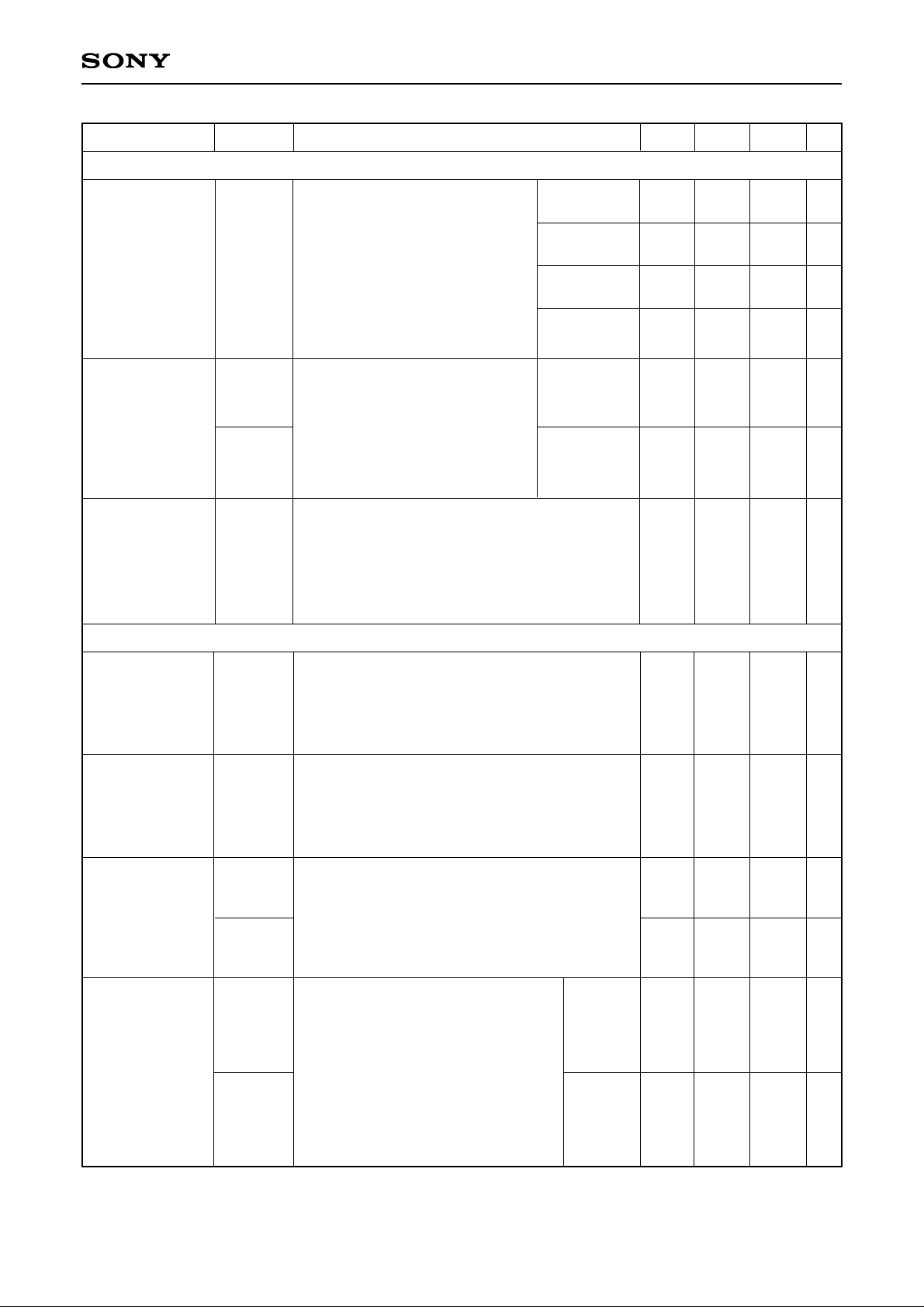
Input SIG5 (VL = 0mV, VS = 143mV, WS variable) to
(A) and confirm that it is synchronized with the HD
output at TP21. Gradually narrow the WS of SIG5
from 4.7µs and obtain the WS at which
synchronization with the HD output at TP21 is lost.
Input SIG5 (VL = 0mV, WS = 4.7µs, VS variable) to
(A) and confirm that it is synchronized with the HD
output at TP21. Gradually reduce the VS of SIG5 from
143mV and obtain the VS at which synchronization
with the HD output at TP21 is lost.
Input SIG5 (VL = 0mV, WS = 4.7µs, VS = 143mV) to
(A) and measure the delay time with the HD output at
TP21. TDSY1 is from the falling edge of the input
HSYNC to the rising edge of the HD output, and
TDSY2 is from the falling edge of the input HSYNC to
the falling edge of the HD output.
Input SIG5 (VL = 0mV, WS = 4.7µs, VS =
143mV, horizontal frequency variable) to
(A) and confirm that it is synchronized
with the HD output at TP21. Obtain the
frequency f
H at which the input and
output are synchronized by changing the
horizontal frequency of SIG5 from the
non-synchronized condition.
HPLLN = f
H – 15734, HPLLP = fH – 15625
– 18 –
CXA3017R
Item Symbol Conditions Min. Typ. Max. Unit
ATBPF
ATRAPN
ATRAPP
DEMLPF
–18
–12
dB
–16 –10 dB
–6 –2 dB
–6
–2 dB
–40 –30 dB
–40
–30
dB
0.9
1.2
1.5 MHz
NTSC 1.5MHz
PAL 2.0MHz
NTSC 5.5MHz
PAL 6.8MHz
NTSC
PAL
Amount of BPF
attenuation
Amount of TRAP
attenuation
R-Y and B-Y LPF
characteristics
Filter characteristics
Assume the chroma amplitude at
TP55 when SIG5 (VL = 0mV) is input
to (A) and SIG1 (0dB at input center
frequency (3.58MHz or 4.43MHz)) is
input to (B) as 0dB. Obtain the
amount by which the output at TP55
is attenuated when the frequencies
noted on the right are input.
SW57 = A
Input SIG2 (0dB, 3.58MHz and
4.43MHz) to (A) and measure the
output at TP43 with a spectrum
analyzer. Assume the amplitude at
TP43 during Y/C input mode as 0dB,
and obtain the amount of attenuation
during COMP input mode.
Assume the amplitude of the 100kHz component of
the output at TP43 when SIG5 (VL = 150mV) is input
to (A) and SIG2 (0dB, 3.58MHz + 100kHz) is input to
(B) as 0dB. Obtain the frequency which attenuates
the beat component of the output by 3dB when the
SIG2 frequency is increased with respect to 3.58MHz.
Page 19
– 19 –
CXA3017R
Item Symbol Conditions Min. Typ. Max. Unit
tTLH
tTHL
∆T
DTYHC
30
ns
30
ns
10
ns
47 50 53
%
Output transition
time
(page 11
∗
2
pins)
Cross-point time
difference
HCK duty
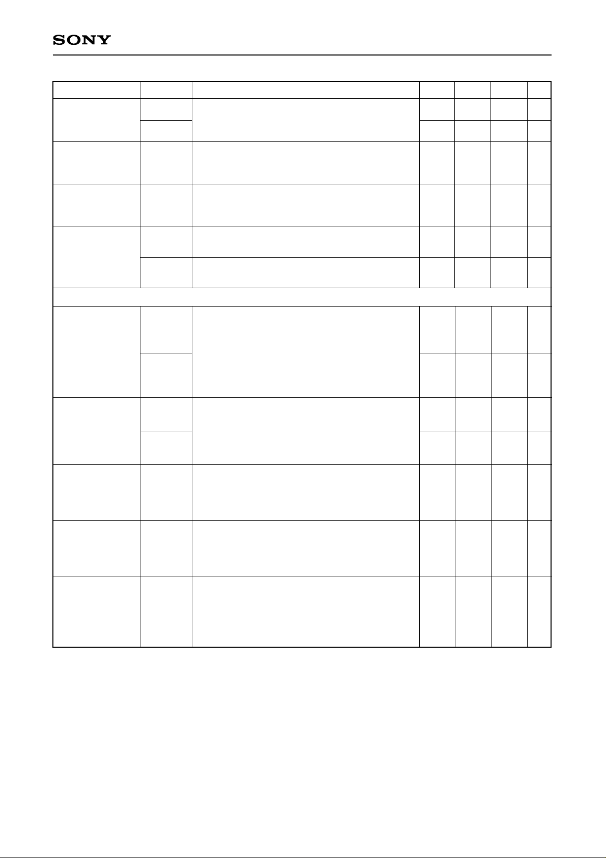
Input SIG5 (VL = 0mV) to (A) and measure the
transition time for each output.
Load = 50pF (See Fig. 3.) SW57 = A
Input SIG5 (VL = 0mV) to (A) and measure
HCK1/HCK2, VCK1/VCK2 and VCK3/VCK4.
Load = 50pF (See Fig. 4.) SW57 = A
Input SIG5 (VL = 0mV) to (A) and measure the
HCK1/HCK2 duty.
Load = 50pF, SW57 = A
2.7
V
VBKLTH
DA OUT output
voltage
Measure the output voltage at TP23 when DA OUT = 7.
I
OH = –1mA
0.3
V
VBKLTL
Measure the output voltage at TP23 when DA OUT = 0.
I
OH = 1mA
EXTWT
3.0
V
180
ns
Input SIG5 (VL = 0mV) to (A) and SIG6 (VL = 2.7V) to
(C). Measure the difference from the black level of the
outputs at TP40, TP43 and TP45.
SW1 = SW2 = SW3 = B
TEXMIN
Input SIG5 (VL = 0mV) to (A) and SIG6 (VL = 2.7V) to
(C). Measure the minimum pulse width at which each
of the outputs at TP40, TP43 and TP45 reach the
white limiter.
SW1 = SW2 = SW3 = B
Output white level
during external
RGB input
Minimum pulse
width during
external RGB input
VTEXTB
VTEXTW
TD1EXT
TD2EXT
0.8 1.0 1.2
V
1.8
2.0 2.2
V
50 90
130
ns
50 100 140
ns
Input SIG5 (VL = 0mV) to (A) and SIG6 (VL variable) to
(C). Raise the SIG6 amplitude (VL) from 0V and assume
the voltage where the outputs at TP40, TP43 and TP45
go to black level as VTEXTB. Then raise the amplitude
further and assume the voltage where these outputs go
to white level as VTEXTW.
SW1 = SW2 = SW3 = B
Input SIG5 (VL = 0mV) to (A) and SIG6 (VL = 3V) to (C).
Measure the rise delay time TD1EXT and the fall delay
time TD2EXT of the outputs at TP40, TP43 and TP45.
(See Fig. 2.)
SW1 = SW2 = SW3 = B
External I/O characteristics
External RGB input
threshold voltage
Propagation delay
time between
external RGB input
and output
EXTBK
0
V
Input SIG5 (VL = 0mV) to (A) and SIG6 (VL = 1.7V) to
(C). Measure the difference from the black level of the
outputs at TP40, TP43 and TP45.
SW1 = SW2 = SW3 = B
Output blanking
level during
external RGB input
Page 20
– 20 –
CXA3017R
Item Symbol Conditions Min. Typ. Max. Unit
LOAD setup time, activated by the rising edge of SCLK.
(See Fig. 6.)
DATA setup time, activated by the rising edge of SCLK.
(See Fig. 6.)
LOAD hold time, activated by the rising edge of SCLK.
(See Fig. 6.)
DATA hold time, activated by the rising edge of SCLK.
(See Fig. 6.)
SCLK pulse width. (See Fig. 6.)
SCLK pulse width. (See Fig. 6.)
LOAD pulse width. (See Fig. 6.)
150
150
150
150
156
156
1
ns
ns
ns
ns
ns
ns
µs
ts0
ts1
th0
th1
tw1L
tw1H
tw2
Serial transfer block
Data setup time
Data hold time
Minimum pulse
width
Page 21
– 21 –
CXA3017R
Setting 2
Current characteristics
Digital block I/O characteristics
Y signal block
Description of Electrical Characteristics Measurement Methods
Serial Bus Register Initial Settings
Item
Symbol
Serial bus
Mode settings
Input
System
Panel
S/H HUE COL BRT CNT
R-
BRT
B-
BRT
γ1
γ2
DAC settings
Low level input
voltage
High level input
voltage
High level output
voltage
Low level output
voltage
Video maximum
gain
Contrast
characteristics TYP
Contrast
characteristics MIN
I
CC11
ICC12
I
CC13ICC2IDD1
IDD2
VIL
VIH
VOH1
VOL1
GV
GCNTTP
GCNTMN
COMP
COMP
Y/C
Y/color
difference
COMP
COMP
COMP
COMP
COMP
COMP
COMP
COMP
COMP
COMP
NTSC
NTSC
NTSC
NTSC
NTSC
NTSC
NTSC
NTSC
NTSC
NTSC
NTSC
NTSC
NTSC
NTSC
—
—
—
—
501
009
005
—
—
—
—
—
—
—
1
1
1
1
1
1
1
1
1
1
1
ALL
ALL
ALL
FRP
ON
ON
ON
ON
ON
ON
ON
ON
ON
ON
ON
ON
ON
ON
128
128
128
128
128
128
128
128
128
128
128
128
128
128
128
128
128
128
128
128
128
128
128
128
128
128
128
128
128
128
128
128
128
128
128
128
128
128
128
128
128
128
128
128
128
128
128
128
128
128
128
128
128
255
128
0
128
128
128
128
128
128
128
128
128
128
128
128
128
128
128
128
128
128
128
128
128
128
128
128
128
128
128
128
0
0
0
0
0
0
0
0
0
0
0
0
0
0
0
0
0
0
0
0
0
0
0
0
0
0
0
0
VCO
ADJ
ADJ
ADJ
ADJ
ADJ
ADJ
ADJ
ADJ
ADJ
ADJ
ADJ
ADJ
ADJ
ADJ
PIC
128
128
128
128
128
128
128
128
128
128
128
128
128
128
BLK
LIM
0
0
0
0
0
0
0
0
0
0
0
0
0
0
WHITE
LIM
3
3
3
3
3
3
3
3
3
3
3
3
3
3
USER
-BRT
128
128
128
128
128
128
128
128
128
128
128
128
128
128
R-
CNT
128
128
128
128
128
128
128
128
128
128
128
128
128
128
B-
CNT
128
128
128
128
128
128
128
128
128
128
128
128
128
128
PSIG
BRT
128
128
128
128
128
128
128
128
128
128
128
128
128
128
DA
OUT
—
—
—
—
—
—
—
—
—
—
—
—
—
—
(—: don't care, ADJ: adjustment, SET: setting)
VCO must be reset when the panel mode is changed.
Horizontal AFC
adjustment
Current
consumption V
CC1
Current
consumption V
CC2, 3
Current
consumption V
DD1, 2
Page 22
– 22 –
CXA3017R
Y signal blockChroma signal block
Item
Symbol
Serial bus
Mode settings
Input
System
Panel
S/H HUE
COL BRT CNT
R-
BRT
B-
BRT
γ1
γ2
DAC settings
Y signal frequency
response
Carrier leak (Y block)
Y signal I/O delay
tim
e
ACC amplitude
characteristics 1
ACC amplitude
characteristics 2
APC pull-in range
FCYYC
FCYCMN
FCYCMP
GSHP1X
GSHP1N
GSHP2X
GSHP2N
GSHP3X
GSHP3N
GSHP4X
GSHP4N
CRLEKY
TDYYC
TDYCMN
TDYCMP
TDYDEF
ACC1
ACC2
FAPC
Y/C
COMP
COMP
Y/C
Y/C
Y/C
Y/C
COMP
COMP
COMP
COMP
COMP
Y/C
COMP
COMP
Y/color
difference
COMP
COMP
COMP
COMP
COMP
COMP
NTSC
NTSC
SPAL
NTSC
NTSC
NTSC
NTSC
NTSC
NTSC
NTSC
NTSC
—
—
NTSC
SPAL
—
NTSC
SPAL
NTSC
SPAL
NTSC
SPAL
009
005
005
009
009
005
005
005
005
009
009
—
—
—
—
—
—
—
—
—
—
—
ALL
ALL
ALL
ALL
ALL
ALL
ALL
ALL
ALL
ALL
ALL
ALL
ALL
ALL
ALL
ALL
ALL
ALL
ALL
ALL
ALL
ALL
FRP
ON
ON
ON
ON
ON
ON
ON
ON
ON
ON
ON
ON
ON
ON
ON
ON
ON
ON
ON
ON
ON
ON
128
128
128
128
128
128
128
128
128
128
128
128
128
128
128
128
128
128
128
128
128
128
128
128
128
128
128
128
128
128
128
128
128
128
128
128
128
128
128
128
128
128
128
128
128
128
128
128
128
128
128
128
128
128
128
128
128
128
128
128
128
128
128
128
128
128
128
128
128
128
128
128
128
128
128
128
128
128
128
128
128
128
128
128
128
128
128
128
128
128
128
128
128
128
128
128
128
128
128
128
128
128
128
128
128
128
128
128
128
128
180
128
128
128
128
128
128
128
128
128
128
128
128
128
128
128
128
128
128
128
128
128
0
0
0
0
0
0
0
0
0
0
0
0
0
0
0
0
0
0
0
0
0
0
0
0
0
0
0
0
0
0
0
0
0
0
0
0
0
0
0
0
0
0
0
0
VCO
ADJ
ADJ
ADJ
ADJ
ADJ
ADJ
ADJ
ADJ
ADJ
ADJ
ADJ
ADJ
ADJ
ADJ
ADJ
ADJ
ADJ
ADJ
ADJ
ADJ
ADJ
ADJ
PIC
180
128
128
255
0
255
0
255
0
255
0
128
128
128
128
128
128
128
128
128
128
128
BLK
LIM
0
0
0
0
0
0
0
0
0
0
0
0
0
0
0
0
0
0
0
0
0
0
WHITE
LIM
3
3
3
3
3
3
3
3
3
3
3
3
3
3
3
3
3
3
3
3
3
3
USER
-BRT
128
128
128
128
128
128
128
128
128
128
128
128
128
128
128
128
128
128
128
128
128
128
R-
CNT
128
128
128
128
128
128
128
128
128
128
128
128
128
128
128
128
128
128
128
128
128
128
B-
CNT
128
128
128
128
128
128
128
128
128
128
128
128
128
128
128
128
128
128
128
128
128
128
PSIG
BRT
128
128
128
128
128
128
128
128
128
128
128
128
128
128
128
128
128
128
128
128
128
128
DA
OUT
—
—
—
—
—
—
—
—
—
—
—
—
—
—
—
—
—
—
—
—
—
—
(—: don't care, ADJ: adjustment, SET: setting)VCO must be reset when the panel mode is changed.
Picture quality
adjustment variable
amount 1
Picture quality
adjustment variable
amount 2
Picture quality
adjustment variable
amount 3
Picture quality
adjustment variable
amount 4
Page 23

– 23 –
CXA3017R
Chroma signal block
Item
Symbol
Serial bus
Mode settings
Input
System
Panel
S/H HUE COL BRT CNT
R-
BRT
B-
BRT
γ1
γ2
DAC settings
Color adjustment
characteristics MAX
Color adjustment
characteristics MIN
HUE adjustment
characteristics MAX
HUE adjustment
characteristics MIN
Killer operation
input level
Color difference
input color
adjustment
Color difference
balance
GCOLMX
GCOLMN
HUEMX
HUEMN
ACKN
ACKP
VRBN
VGBN
θRBN
θGBN
VRBP
VGBP
θRBP
θGBP
GEXCMX
GEXCMN
VEXCBL
COMP
COMP
COMP
COMP
COMP
COMP
COMP
COMP
COMP
COMP
COMP
COMP
COMP
COMP
Y/color
difference
Y/color
difference
Y/color
difference
NTSC
NTSC
NTSC
NTSC
NTSC
SPAL
NTSC
NTSC
NTSC
NTSC
SPAL
SPAL
SPAL
SPAL
—
—
—
—
—
—
—
—
—
—
—
—
—
—
—
—
—
—
—
—
ALL
ALL
ALL
ALL
ALL
ALL
ALL
ALL
ALL
ALL
ALL
ALL
ALL
ALL
ALL
ALL
ALL
FRP
ON
ON
ON
ON
ON
ON
ON
ON
ON
ON
ON
ON
ON
ON
ON
ON
ON
128
128
255
0
128
128
128
128
128
128
128
128
128
128
128
128
128
255
0
128
128
128
128
128
128
128
128
128
128
128
128
255
0
128
128
128
150
150
150
150
150
150
150
150
150
150
150
150
128
128
128
128
128
128
128
128
128
128
128
128
128
128
128
128
128
128
128
128
128
128
128
128
128
128
128
128
128
128
128
128
128
128
128
128
128
128
128
128
128
128
128
128
128
128
128
128
128
128
128
128
128
128
0
0
0
0
0
0
0
0
0
0
0
0
0
0
0
0
0
0
0
0
0
0
0
0
0
0
0
0
0
0
0
0
0
0
VCO
ADJ
ADJ
ADJ
ADJ
ADJ
ADJ
ADJ
ADJ
ADJ
ADJ
ADJ
ADJ
ADJ
ADJ
ADJ
ADJ
ADJ
PIC
128
128
128
128
128
128
128
128
128
128
128
128
128
128
128
128
128
BLK
LIM
0
0
0
0
0
0
0
0
0
0
0
0
0
0
0
0
0
WHITE
LIM
3
3
3
3
3
3
3
3
3
3
3
3
3
3
3
3
3
USER
-BRT
128
128
128
128
128
128
128
128
128
128
128
128
128
128
128
128
128
R-
CNT
128
128
128
128
128
128
128
128
128
128
128
128
128
128
128
128
128
B-
CNT
128
128
128
128
128
128
128
128
128
128
128
128
128
128
128
128
128
PSIG
BRT
128
128
128
128
128
128
128
128
128
128
128
128
128
128
128
128
128
DA
OUT
—
—
—
—
—
—
—
—
—
—
—
—
—
—
—
—
—
(—: don't care, ADJ: adjustment, SET: setting)VCO must be reset when the panel mode is changed.
Demodulation
output amplitude
ratio (NTSC)
Demodulation
output phase
difference (NTSC)
Demodulation
output amplitude
ratio (PAL)
Demodulation
output phase
difference (PAL)
Page 24

– 24 –
CXA3017R
RGB signal output block
Item
Symbol
Serial bus
Mode settings
Input
System
Panel
S/H HUE COL BRT CNT
R-
BRT
B-
BRT
γ1
γ2
DAC settings
Color difference
input balance
adjustment R
Color difference
input balance
adjustment B
G-Y matrix
characteristics
(NTSC)
G-Y matrix
characteristics
(PAL)
RGB/PSIG output
DC voltage
RGB/PSIG output
DC voltage difference
SIG center variable
range
Amount of change
in PSIG output
GEXRMX
GEXRMN
GEXBMX
GEXBMN
VEXGBN
VEXGRN
VEXGBP
VEXGRP
VOUT
∆
VOUT
VORNG
VLIMMX
VLIMMN
PSIGMX
PSIGMN
Y/color
difference
Y/color
difference
Y/color
difference
Y/color
difference
Y/color
difference
Y/color
difference
Y/color
difference
Y/color
difference
—
—
—
—
—
—
—
—
—
—
—
NTSC
NTSC
SPAL
SPAL
—
—
—
—
—
—
—
—
—
—
—
—
—
—
—
—
—
—
—
—
—
—
ALL
ALL
ALL
ALL
ALL
ALL
ALL
ALL
ALL
ALL
ALL
ALL
ALL
ALL
ALL
FRP
ON
ON
ON
ON
ON
ON
ON
ON
ON
ON
ON
ON
ON
ON
ON
255
0
255
0
128
128
128
128
128
128
128
128
128
128
128
128
128
128
128
128
128
128
128
128
128
128
128
128
128
128
128
128
128
128
128
128
128
128
ADJ
ADJ
ADJ
80
80
128
128
128
128
128
128
128
128
128
128
128
128
128
255
255
255
255
128
128
128
128
128
128
128
128
128
128
128
128
128
128
128
128
128
128
128
128
128
128
128
128
128
128
128
128
128
128
0
0
0
0
0
0
0
0
0
0
0
0
0
0
0
0
0
0
0
0
0
0
0
0
0
0
0
0
0
0
VCO
ADJ
ADJ
ADJ
ADJ
ADJ
ADJ
ADJ
ADJ
ADJ
ADJ
ADJ
ADJ
ADJ
ADJ
ADJ
PIC
128
128
128
128
128
128
128
128
128
128
128
128
128
128
128
BLK
LIM
0
0
0
0
0
0
0
0
0
0
0
0
255
0
0
WHITE
LIM
3
3
3
3
3
3
3
3
3
3
3
3
3
3
3
USER
-BRT
128
128
128
128
128
128
128
128
128
128
128
128
128
128
128
R-
CNT
128
128
128
128
128
128
128
128
128
128
128
128
128
128
128
B-
CNT
128
128
128
128
128
128
128
128
128
128
128
128
128
128
128
PSIG
BRT
128
128
128
128
128
128
128
128
128
128
128
128
128
255
0
DA
OUT
—
—
—
—
—
—
—
—
—
—
—
—
—
—
—
(—: don't care, ADJ: adjustment, SET: setting)VCO must be reset when the panel mode is changed.
RGB output/PSIG
black limiter
operation voltage
Chroma signal block
Page 25

– 25 –
CXA3017R
RGB signal output block
Item
Symbol
Serial bus
Mode settings DAC settings
Amount of change
in user brightness
Amount of change
in brightness
Amount of change
in sub brightness
Difference in gain
between RGB signals
Amount of change
in sub-contrast
Difference in RGB
inverted/non-inverted
gain
Difference in black
level potential
between RGB signals
γ gain
γ1 adjustment
variable range
γ2 adjustment
variable range
PSIG transition time
UBRTMX
UBRTMN
BRTMX
BRTMN
SBBRT
∆GRGB
SBCNT
∆GINV
∆VBL
Gγ1
Gγ2
Gγ3
V
γ
1MN
V
γ
1MX
V
γ
2MN
V
γ
2MX
tPSIG
—
—
—
—
—
—
—
—
—
—
—
—
—
—
—
—
—
—
—
—
—
—
—
—
—
—
—
—
—
—
—
—
—
—
—
—
—
—
—
—
—
—
—
—
—
—
—
—
—
—
—
ALL
ALL
ALL
ALL
ALL
ALL
ALL
ALL
ALL
ALL
ALL
ALL
ALL
ALL
ALL
ALL
ALL
ON
ON
ON
ON
ON
ON
ON
ON
ON
ON
ON
ON
ON
ON
ON
ON
ON
128
128
128
128
128
128
128
128
128
128
128
128
128
128
128
128
128
128
128
128
128
128
128
128
128
128
128
128
128
128
128
128
128
128
128
128
255
0
160
128
128
128
128
ADJ
ADJ
ADJ
80
80
80
80
128
255
255
255
255
128
128
128
128
128
ADJ
ADJ
ADJ
60
60
60
60
128
128
128
128
128
SET
128
128
128
128
128
128
128
128
128
128
128
128
128
128
128
128
SET
128
128
128
128
128
128
128
128
128
128
128
128
0
0
0
0
0
0
0
0
0
140
140
140
0
255
0
0
128
0
0
0
0
0
0
0
0
0
230
230
230
0
0
0
255
128
ADJ
ADJ
ADJ
ADJ
ADJ
ADJ
ADJ
ADJ
ADJ
ADJ
ADJ
ADJ
ADJ
ADJ
ADJ
ADJ
ADJ
128
128
128
128
128
128
128
128
128
128
128
128
128
128
128
128
128
0
0
0
0
0
0
0
0
0
0
0
0
0
0
0
0
0
3
3
3
3
3
3
3
3
3
3
3
3
3
3
3
3
3
255
0
128
128
128
128
128
128
128
128
128
128
128
128
128
128
128
128
128
128
128
128
128
SET
128
128
128
128
128
128
128
128
128
128
128
128
128
128
128
128
SET
128
128
128
128
128
128
128
128
128
128
128
128
128
128
128
128
128
128
128
128
128
128
128
128
128
128
SET
—
—
—
—
—
—
—
—
—
—
—
—
—
—
—
—
—
(—: don't care, ADJ: adjustment, SET: setting)VCO must be reset when the panel mode is changed.
Input
System
Panel
S/H HUE COL BRT CNT
R-
BRT
B-
BRT
γ1
γ2
FRP
VCOPIC
BLK
LIM
WHITE
LIM
USER
-BRT
R-
CNT
B-
CNT
PSIG
BRT
DA
OUT
Page 26

– 26 –
CXA3017R
Item
Symbol
Serial bus
Mode settings DAC settings
RGB output white
limiter operation
voltage
Black limiter DC
voltage difference
White limiter DC
voltage difference
RGB output range
when FRP polarity
inversion is stopped
Amount of BPF
attenuation
Amount of TRAP
attenuation
R-Y and B-Y LPF
characteristics
Input sync signal
width sensitivity
Sync separation
input sensitivity
HD output delay
time
Horizontal pull-in
range
Output transition
time
VWLIM
∆
VBLIM
∆
VWLIM
VDROFF
ATBPF
ATRAPN
ATRAPP
DEMLPF
WSSEP
VSSEP
TDSY1
TDSY2
HPLLN
HPLLP
tTLH
tTHL
—
—
—
—
COMP
SET
SET
Y/C
—
—
—
—
—
—
COMP
COMP
—
—
—
—
SET
NTSC
SPAL
NTSC
—
—
NTSC
NTSC
NTSC
SPAL
NTSC
NTSC
—
—
—
—
—
—
—
—
—
—
009
009
—
—
—
—
ALL
ALL
ALL
ALL
ALL
ALL
ALL
ALL
ALL
ALL
ALL
ALL
ALL
ALL
1
1
ON
ON
ON
OFF
ON
ON
ON
ON
ON
ON
ON
ON
ON
ON
ON
ON
128
128
128
128
128
128
128
128
128
128
128
128
128
128
128
128
128
128
128
128
128
128
128
128
128
128
128
128
128
128
128
128
128
0
255
SET
128
128
128
150
128
128
128
128
128
128
128
128
128
128
128
128
128
128
128
128
128
128
128
128
128
128
128
128
128
128
128
128
128
128
128
128
128
128
128
128
128
128
128
128
128
128
128
128
128
128
128
128
128
128
128
128
128
128
128
128
0
0
0
0
0
0
0
0
0
0
0
0
0
0
0
0
255
0
0
0
0
0
0
0
0
0
0
0
0
0
0
0
ADJ
ADJ
ADJ
ADJ
ADJ
ADJ
ADJ
ADJ
ADJ
ADJ
ADJ
ADJ
ADJ
ADJ
ADJ
ADJ
128
128
128
128
128
128
128
128
128
128
128
128
128
128
128
128
0
ADJ
0
0
0
0
0
0
0
0
0
0
0
0
0
0
SET
0
0
3
3
3
3
3
3
3
3
3
3
3
3
3
0
128
128
0
128
128
128
128
128
128
128
128
128
128
128
128
128
128
128
128
128
128
128
128
128
128
128
128
128
128
128
128
128
128
128
128
128
128
128
128
128
128
128
128
128
128
128
128
128
128
128
128
128
128
128
128
128
128
128
128
128
128
128
128
—
—
—
—
—
—
—
—
—
—
—
—
—
—
—
—
(—: don't care, ADJ: adjustment, SET: setting)
VCO must be reset when the panel mode is changed.
Sync, TG block Filter characteristics
Input
System
Panel
S/H HUE COL BRT CNT
R-
BRT
B-
BRT
γ1
γ2
FRP
VCOPIC
BLK
LIM
WHITE
LIM
USER
-BRT
R-
CNT
B-
CNT
PSIG
BRT
DA
OUT
RGB signal output block
Page 27

– 27 –
CXA3017R
Item
Symbol
Serial bus
Mode settings DAC settings
Cross-point time
difference
HCK duty
DA OUT output
voltage
External RGB input
threshold voltage
External RGB input
blanking level
External RGB input
output white level
External RGB input
minimum pulse width
∆T
DTYHC
VBKLTH
VBKLTL
VTEXTB
VTEXTW
TD1EXT
TD2EXT
EXTBK
EXTWT
TEXMIN
COMP
COMP
—
—
—
—
—
—
—
—
—
NTSC
NTSC
—
—
—
—
—
—
—
—
—
—
—
—
—
—
—
—
—
—
—
—
1
1
—
—
ALL
ALL
ALL
ALL
ALL
ALL
ALL
ON
ON
—
—
ON
ON
ON
ON
ON
ON
ON
128
128
—
—
128
128
128
128
128
128
128
128
128
—
—
128
128
128
128
128
128
128
128
128
—
—
128
128
128
128
128
100
128
128
128
—
—
128
128
128
128
128
128
128
128
128
—
—
128
128
128
128
128
128
128
128
128
—
—
128
128
128
128
128
128
128
0
0
—
—
0
0
0
0
0
0
0
0
0
—
—
0
0
0
0
0
0
0
ADJ
ADJ
—
—
ADJ
ADJ
ADJ
ADJ
ADJ
ADJ
ADJ
128
128
—
—
128
128
128
128
128
128
128
0
0
—
—
0
0
0
0
0
0
0
3
3
—
—
3
3
3
3
3
3
3
128
128
—
—
128
128
128
128
128
128
128
128
128
—
—
128
128
128
128
128
128
128
128
128
—
—
128
128
128
128
128
128
128
128
128
—
—
128
128
128
128
128
128
128
—
—
7
0
—
—
—
—
—
—
—
(—: don't care, ADJ: adjustment, SET: setting)VCO must be reset when the panel mode is changed.
Sync, TG block
Input
System
Panel
S/H HUE COL BRT CNT
R-
BRT
B-
BRT
γ1
γ2
FRP
VCOPIC
BLK
LIM
WHITE
LIM
USER
-BRT
R-
CNT
B-
CNT
PSIG
BRT
DA
OUT
Propagation delay
time between external
RGB input and output
External I/O characteristics
Page 28

– 28 –
CXA3017R
SIG6
TP40, 43, 45
non-inverted output
TD1EXT TD2EXT
3V
0V
50%
100%
Fig. 2. Conditions for measuring the delay between external RGB input and output
tTLH
90%
tTHL
10%
50%
∆T
∆T
Fig. 3. Output transition time measurement
conditions
Fig. 4. Cross-point time difference measurement
conditions
VG1
Non-inverted output
VG2
VG3
3.5V
White
Black
1.5V
Input
Fig. 5. γ characteristics measurement conditions
Electrical Characteristic Measurement Method Diagrams
Page 29
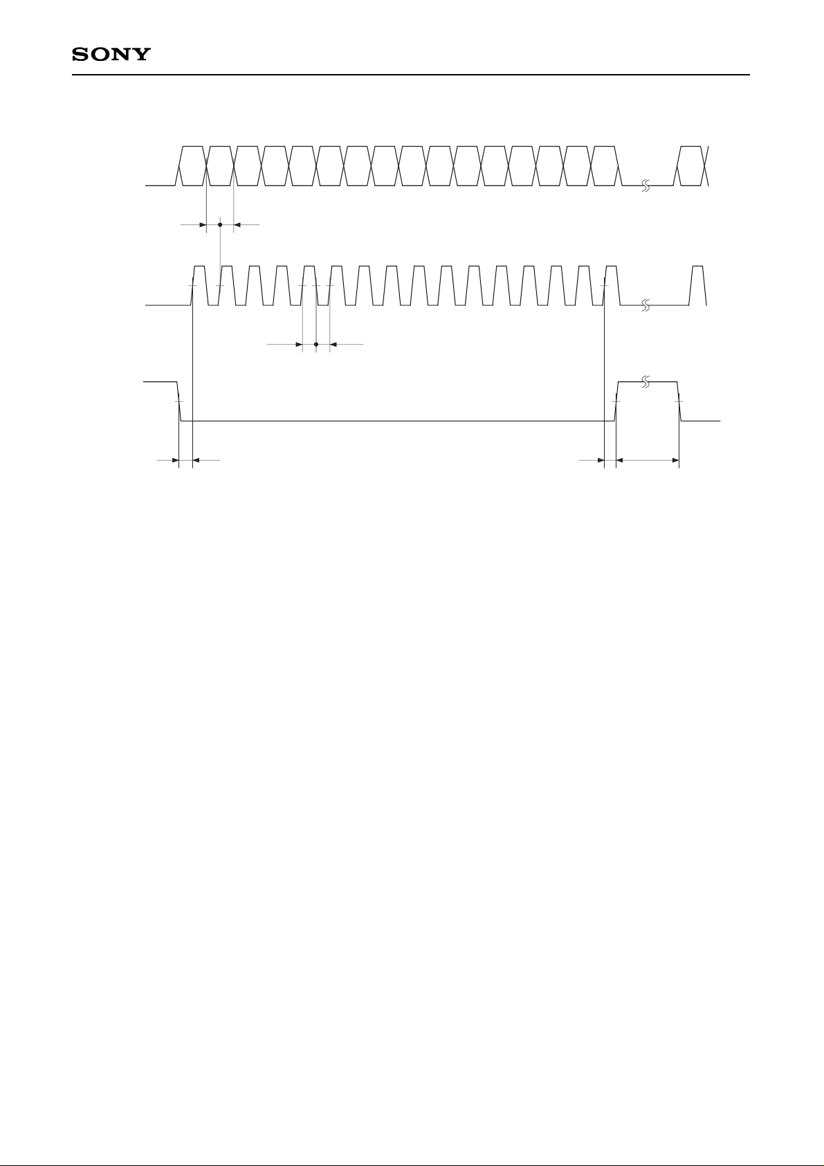
– 29 –
CXA3017R
D15 D14 D13 D12 D11 D10 D9 D8 D7 D6 D5 D4 D3 D2 D1 D0 D15
ts1 th1
tw1H tw1L
50%
DATA
SCLK
50%
th0 tw2ts0
LOAD
Fig. 6. Serial transfer block measurement conditions
Page 30

– 30 –
CXA3017R
Input Waveforms
SG No. Waveform
SIG1
143mV
150mV
150mV
Sine wave video signal: With/without burst
Amplitude and frequency variable
← Value noted
on left: 0 dB
SIG2
SIG3
143mV
150mV
← Value noted
on left: 0 dB
Chroma signal: Burst, chroma frequency (3.579545MHz, 4.433619MHz)
Chroma phase and burst frequency variable
143mV
357mV
Ramp waveform
1H
SIG4
SIG5
143mV
150mV
5-step staircase waveform
1H
VL
VS
WS
VL amplitude variable
VS variable: 143mV unless otherwise specified
WS variable: 4.7µs unless otherwise specified
f
H variable: 15.734kHz (NTSC) or 15.625kHz (PAL)
unless otherwise specified
fH
Page 31

– 31 –
CXA3017R
SG No. Waveform
SIG6
VL
VL amplitude variable
Horizontal sync signal
30µs 5µs
SIG7
143mV
75mV
Frequency variable
175mV
SIG8
143mV
357mV
10-step staircase waveform
1H
SIG9
357mV
143mV
1H
SIN
2
2T pulse waveform
Page 32

– 32 –
CXA3017R
Electrical Characteristics Measurement Circuit
V58
47µ
0.01µ
+12V
0.1µ
47µ 0.01µ
2
3
4
5
6
7
8
9
10
11
12
13
14
15
16
1
46
40
39
38
37
36
35
34
33
41
42
43
44
45
47
48
49
50
51
52
53
54
55
56
57
58
59
60
63
64
61
62
17
18
19
20
21
22
23
24
25
26
27
28
29
30
31
32
16p
0.33µ
+3V
VCC1
VXO IN
APC
B-Y IN
R-Y IN
C OUT
V REG
C IN
RESET
Y IN
TEST2
SYNC IN
VSEP TC
F0 ADJ
GND1
DA OUT
VD
EN2
EN1
XEN1
VCK1
VCK2
VCK3
VCK4
VST
XVST
HD
PCG
XPCG
HCK1
HCK2
V
SS
XHST1
HST1
HST2
CLR
BLK
SCLK
DATA
LOAD
V
DD
1
TRAP
EXT B
EXT G
EXT R
V
DD
2
DWN
RGT1
FB PSIG
GND3
PSIG
V
CC
3
B OUT
FB B
GND2
FB G
R OUT
FB R
V
CC
2
SIG.CENTER
VXO OUT
RPD
TEST1
G OUT
(C)
TP32
TP31
TP30
TP29
TP28
TP27
TP26
TP25
TP24
TP23
TP22
TP21
TP20
TP19
TP18
TP17
TP6 TP7 TP8
TP10 TP11 TP12 TP14 TP15TP13
10k
3.3µ
6800p
TP9
A
B
SW2
A
B
SW3
A
B
SW1
47µ 0.01µ
+3V
IDD4
A
IDD3
A
∗
3
ICC2
A
0.1µ
0.1µ
0.1µ
0.01µ
400p
TP43
400p
TP40
20000p
TP38
+15.5V
100k
100k
TP35
TP34
SW48
V48
47µ
0.01µ
+3V
ICC1
A
∗
2
15k
0.01µ
1µ
1µ
TP60
(A)
SW58
(B)
A
B
SW57
TP55
(E)
A
B
0.1µ
A
B
0.1µ
SW54
SW53
∗
1
0.22µ
0.033µ
10k
400p
TP45
(D)
3.9k
∗1
Used crystal: KINSEKI CX-5F
Frequency deviation: within ±30ppm,
frequency temperature characteristics: within ±30ppm,
load capacity: 16pF
NTSC: 3.579545MHz
PAL: 4.433619MHz
∗2
Resistance value tolerance: ±2%,
temperature coefficient: ±200ppm or less
∗3
Trap (TDK)
NTSC: NLT4532-S3R6B
PAL: NLT4532-S4R4
Page 33

– 33 –
CXA3017R
Description of Operation
The CXA3017R incorporates the three functions of an RGB decoder block, an RGB driver block and a timing
generator (TG) block onto a single chip using Bi-CMOS technology.
1) RGB decoder block
• Input mode switching
The input mode (composite input, Y/C input, Y/color difference input) can be switched by the serial bus settings.
During composite input: The composite signal is input to Pins 57, 59 and 61.
During Y/C input: The Y signal is input to Pins 59 and 61, and the C signal to Pin 57.
During Y/color difference input: The Y signal is input to Pins 59 and 61, the B-Y signal to Pin 53, and the R-Y
signal to Pin 54.
• System switching
The input system (NTSC, SPAL, DPAL) can be switched by the serial bus settings. (DPAL uses external
delay lines.)
• Trap, BPF
The center frequency of the built-in trap and BPF can be switched to 3.58MHz during NTSC and 4.43MHz
during PAL.
During composite input, the Y signal enters the trap circuit and the C signal enters the BPF. These signals do
not pass through the trap or BPF during Y/C input and Y/color difference input.
• ACC detection, ACC amplifier
The amplitude of the burst signal output from the ACC amplifier is detected and the ACC amplifier is controlled
to maintain the burst signal amplitude at a constant level.
• VXO, APC detection
The VXO local oscillation circuit is a crystal oscillation circuit. The phases of the input burst signal and the
VXO oscillator output are compared in the APC detection block, and the detective output is used to form a
PLL that controls the VXO oscillation frequency, which means that the need for adjustments is eliminated.
• External inputs
These are digital inputs with two thresholds. When one of the RGB inputs is higher than the lower threshold
Vth1 (≈ 1.0V), all RGB outputs go to black level. When the higher threshold Vth2 (≈ 2.0V) is exceeded, the
output for only the signal in question goes to white level, while the other outputs remain at black level.
Page 34
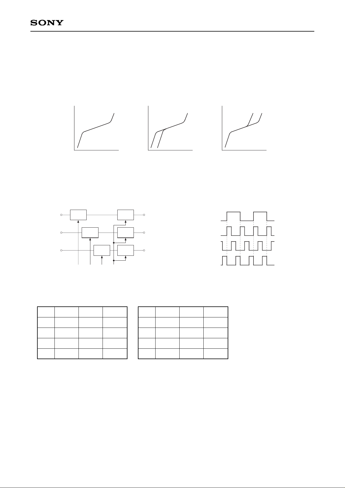
– 34 –
CXA3017R
• Sample-and-hold circuit
As LCD panels sample RGB signals simultaneously, RGB signals output from the CXA3017R must be
sampled-and-held in sync with the LCD panel drive pulses.
S/H4
S/H4
S/H4
G
R
B
S/H2
SH2
S/H1
SH1
S/H3
SH3 SH4
HCK1
A
B
C
2) RGB driver block
• γ correction
In order to support the characteristics of LCD panels, the I/O characteristics are as shown in Fig. 1. The γ gain
transition point A voltage changes as shown in Fig. 2 by adjusting the serial bus register γ1, and the transition
point B voltage changes as shown in Fig. 3 by adjusting γ2.
Input
Output
Fig. 1
A
B
Input
Output
Fig. 2
A
B
Input
Output
Fig. 3
A'
B'
A
B
SH1: R signal SH pulse
SH2: G signal SH pulse
SH3: B signal SH pulse
SH4: RGB signal SH pulse
SHS1,2,3: Serial data settings
The sample-and-hold circuit performs sample and hold by receiving the SH1 to SH4 pulses from the TG
block. Since LCD panels perform color coding using an RGB delta arrangement, each horizontal line must
be compensated by 1.5 dots. This relationship is reversed during right/left inversion. This compensation
timing is also generated by the TG block. The sample-and-hold timing changes according to the phase
relationship with the HCK1 pulse, so the timing should be set to SHS1, 2 or 3 in accordance with the actual
board.
RGT = H (normal)
SHS1
SH1
SH2
SH3
SH4
B
Through
A
C
A
Through
C
B
C
Through
B
A
SHS2 SHS3
RGT = L (right/left inversion)
SHS1
SH1
SH2
SH3
SH4
B
A
Through
C
A
C
Through
B
C
B
Through
A
SHS2 SHS3
Page 35

– 35 –
CXA3017R
• RGB output
RGB outputs (Pins 40, 43 and 45) are inverted each horizontal line by the FRP pulse (internal pulse) supplied
from the TG block as shown in the figure below. Feedback is applied so that the center voltage (Vsig center)
of the output signal matches the reference voltage (VCC2 + GND2)/2 (or the voltage input to SIG CENTER
(Pin 48)). In addition, the white level output is clipped at the limiter operation point that is set by the serial bus
register WHITE LIM, and the black level output is clipped at the limiter operation point that is set by the serial
bus register BLKLIM.
Video IN
FRP
RGB OUT
Black level limiter
White level limiter
White level limiter
Black level limiter
Vsig center
3) TG block
• PLL and AFC circuits
The TG block contains a PLL circuit phase comparator and frequency division counter and a VCO circuit, and
comprises a PLL circuit.
The PLL error detection signal is generated by the HSYNC block, and the integral value of the phase comparison
output of the entire bottom of HSYNC and the internal frequency division counter becomes RPD (Pin 9).
The CXA3017R controls the internal VCO with the RPD output to stabilize the oscillation frequency at 690fH
(NTSC) or 716fH (PAL) for the LCX005BK/BKB and LCX024AK/AKB, and 1034fH (NTSC) or 1072fH (PAL) for
the LCX009AK/AKB, LCX027AK/AKB and DCX501BK. The PLL of this system is adjusted by adjusting the
serial bus register VCO so that the RPD output waveform is constant near VSYNC as shown in the figure
Adjust to a horizontal waveform.
Video signal
RPD (Pin 9)
Horizontal AFC adjustment
• H position
The horizontal display position can be set at 2fH intervals in 32 different ways by the serial bus settings. Note
that the delay difference between the RGB signal and the drive pulse differs according to the board, so adjust
the serial bus register H position so that the picture center matches the center of the LCD panel.
Page 36

– 36 –
CXA3017R
• Wide mode
Wide mode can be selected by setting wide mode with the serial bus aspect switching register. In this mode,
aspect ratio conversion is performed by pulse elimination processing to enable 16:9 quasi-WIDE display.
Vertical pulse elimination scanning of 1/4 for NTSC and 10/28 for PAL is performed and the video signal is
compressed in order to achieve a 16:9 aspect ratio during the wide mode period. In addition, high-speed
scan is performed in areas outside of the active area to display black in the upper 28 lines and the lower 28
(27) lines. Black display is performed by limiting the video signal input during the V blanking period and
writing a black level signal in its place.
• Right/left inversion
The LCD panel is arranged in a delta arrangement, where identical signal lines are offset by 1.5 dots from
adjoining lines. For this reason, a 1.5-bit offset is attached to the horizontal start pulse (HST) between odd
lines and even lines. HCK and S/H are also 1.5-bit offset. Therefore, when the panel is driven by left scan
(Reverse scan), this offset relationship is inverted for even and odd lines.
Moreover, since the dot arrangement is asymmetrical, the HST position is also changed.
RGT = H: Right scan mode
RGT = L: Left scan mode
(H and L are the LCD panel input levels.)
H SCANNER
Left scan
(Reverse scan)
Right scan
(Normal scan)
Active area
V SCANNER
LCD panel
Active area Active area
Black active area
Vertical high-speed scan
Vertical pulse elimination scan
16:9 display4:3 display
225 LINES
(218 LINES)
169 LINES
(163 LINES)
28 LINES
(28 LINES)
28 LINES
(27 LINES)
Black active area
Numbers inside parentheses are for the LCX005BK/BKB and LCX024AK/AKB; other numbers are for the
LCX009AK/AKB, LCX027AK/AKB and DCX501BK.
Page 37

– 37 –
CXA3017R
• AC driving of LCD panels during no signal
HST, XHST, HCK1, HCK2, VST, XVST, VCK1, VCK2, PCG, XPCG, EN, XEN, HD, VD, and FRP (internal
pulse) are made to run freely so that the LCD panel is AC driven even when there is no composite sync from
the SYNCIN pin.
During this time, the HSYNC separation circuit stops and the PLL counter is made to run freely. In addition,
the VSYNC separation circuit is also stopped, so the auxiliary V counter is used to create the reference pulse
for generating VD, VST and XVST. The cycle of this V counter is designed to be 525/2H for NTSC and
625/2H for PAL. However, when there is no vertical sync signal for 5 fields, the no signal state is assumed
and the free running VD, VST and XVST pulses are generated from the next field. In addition, RPD is kept at
high impedance when there is no signal in order to prevent the AFC circuit from causing errors due to phase
comparison.
Page 38
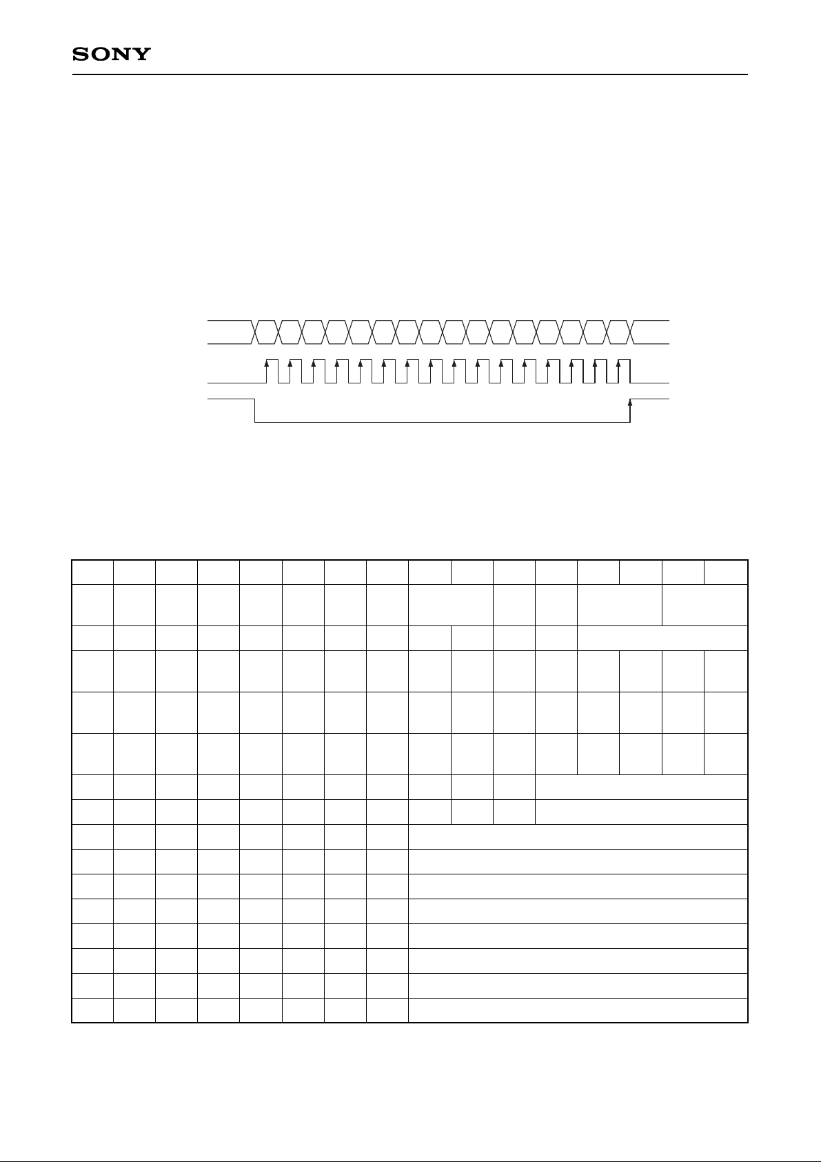
– 38 –
CXA3017R
Description of Serial Control Operation
1) Control method
Control data consists of 16 bits of data which is loaded one bit at a time at the rising edge of SCLK. This
loading operation starts from the falling edge of LOAD and is completed at the next rising edge.
Digital block control data is established by the vertical sync signal, so if data is transferred multiple times for
the same item, the data immediately before the vertical sync signal is valid. Analog (electronic attenuator)
block control data becomes valid each time the LOAD signal is input.
D15 D14 D13 D12 D11 D10 D9 D8 D7 D6 D5 D4 D3 D2 D1 D0
DATA
SCLK
LOAD
Serial transfer timing
2) Serial data map
The serial data map is as follows.
D15
0
0
0
0
0
0
0
1
1
1
1
1
1
1
1
0
0
0
0
0
0
0
0
0
0
0
0
0
0
0
0
0
0
0
0
0
0
0
0
0
0
0
0
0
0
0
0
0
0
0
0
0
0
0
0
0
0
0
0
0
0
0
0
0
0
0
0
0
0
0
0
0
0
0
0
0
0
0
0
1
1
1
0
0
0
0
1
1
1
1
0
0
1
1
0
0
1
0
0
1
1
0
0
1
1
0
1
0
1
0
1
0
0
1
0
1
0
1
0
1
∗
∗
∗
∗
∗
∗
D14 D13 D12 D11 D10 D9 D8 D7 D6 D5 D4 D3 D2 D1 D0
S/H phase
HD-POSITION
H-POSITION
HUE
COLOR
BRIGHT
CONTRAST
R-BRIGHT
B-BRIGHT
γ-1
γ-2
VD
polarity
HD
polarity
External
VSYNC
PLL
adjustment 2
PLL
adjustment 1
0
0
0 0
TEST1
Panel 2
SYNC
GEN
RGT1RGT2DWN
FRP
inversion
P-FRP
inversion
stop
FRP
inversion
stop
TEST2
TEST3
TEST4
TEST5
0
0
0
FRP4096
inversion
POWER
SAVE
Aspect
SYNC
detection
Y/color
difference
clamp
System
Input
switching
Supported panels
∗: don't care
Page 39

– 39 –
CXA3017R
1 1 1 0 0 0 0 0
TEST6
3) Serial data mode settings (X: don't care)
• Input switching
This switches the input signal format.
D1 D0
0 X Composite input (default)
1 0 Y/C input
1 1 Y/color difference input
• System switching
This switches the input video signal system.
D3 D2
0 0 NTSC (default)
0 1 TEST
1 0 D-PAL
1 1 S-PAL
• External VSYNC
Internal VSYNC separation is not performed and an externally input VSYNC is used.
D4
0 OFF (internal separation) (default)
1 ON (external input)
• Aspect switching
This switches the video display aspect.
D5
0 4:3 (normal) (default)
1 16:9 (letterbox, pulse elimination display)
D15
1
1
1
1
1
1
1
1
1
1
1
1
1
1
1
1
1
0
0
0
0
0
1
1
1
1
0
0
0
1
1
0
0
1
1
0
0
1
0
1
0
1
0
1
0
∗
∗
∗
∗
∗
∗
∗
∗
∗
∗
∗
WHITE LIM
DA OUT
0
0
0
0
0
0
0
0
0
0
0
0
0
0
0
0
0
0
0
0
0
0
0
0
0
0
1
D14 D13 D12 D11 D10 D9 D8 D7 D6 D5 D4 D3 D2 D1 D0
PSIG-BRIGHT
R-CONTRAST
B-CONTRAST
BLK LIM
PICTURE
USER-BRIGHT
VCO
∗: don't care
Serial data map (cont.)
Page 40

– 40 –
CXA3017R
D3 D2 D1 D0 Supported panels
0
0
0
0
0
0
0
0
1
1
1
1
1
1
1
1
0
0
0
0
1
1
1
1
0
0
0
0
1
1
1
1
0
0
1
1
0
0
1
1
0
0
1
1
0
0
1
1
0
1
0
1
0
1
0
1
0
1
0
1
0
1
0
1
LCX005BK/BKB single
LCX024AK/AKB single
LCX009AK/AKB single
LCX027AK/AKB single
LCX005BK/BKB + (DCX501BK)
LCX024AK/AKB + (DCX501BK) (default)
LCX009AK/AKB + (DCX501BK)
LCX027AK/AKB + (DCX501BK)
—
DCX501BK single
—
—
DCX501BK + (LCX005BK/BKB)
DCX501BK + (LCX024AK/AKB)
DCX501BK + (LCX009AK/AKB)
DCX501BK + (LCX027AK/AKB)
Two-panel simultaneous drive mode
The supported panels are the main
panel and the sub panel (the panel
noted inside the parentheses).
The video is not displayed correctly on
the sub panel for combinations of the
LCX005BK (BKB)/024AK (AKB) and
the DCX501BK. Therefore, the sub
panel back light should be turned off.
Two-panel simultaneous display is
possible with combinations of the
LCX009AK (AKB)/027AK (AKB) and the
DCX501BK (only when RGT1 = RGT2).
However, when the right/left inversion
directions of the main and sub panels
differ (RGT1 ≠ RGT2), the picture is not
displayed correctly due to the line offset.
Therefore, use Panel 2 mode in these
cases.
• TEST1
This is the test mode. Set to normal mode.
D4
0 Normal mode (default)
1 TEST mode
• Panel 2
Set this when the right/left inversion direction of the two panels differs (RGT1 ≠ RGT2) during two-panel
simultaneous drive using the LCX009AK (AKB)/027AK (AKB)and the DCX501BK.
D5
0 OFF (default)
1 ON
Notes) 1. The VST connection changes in this mode, so an external inverter is required.
2. Set sample and hold to OFF (through) in this mode.
3. When the right/left inversion direction of the two panels differs (RGT1 ≠ RGT2), the video display
start position of the sub panel is advanced by 1H.
4. RGT1 and RGT2 can also be set the same in this mode.
• Sample-and-hold phase
This switches the sample-and-hold timing.
D7 D6
0 0 SHS1 (default)
0 1 SHS2
1 0 SHS3
1 1 Through (sample-and-hold not performed)
• Supported panels
This switches the supported panels.
Page 41

– 41 –
CXA3017R
• HD polarity
This switches the HD output (Pin 21) polarity.
D0
0 Positive polarity (default)
1 Negative polarity
• VD polarity
This switches the VD output (Pin 31) polarity.
D1
0 Positive polarity (default)
1 Negative polarity
• Y/color difference clamp
This switches the position at which the R-Y and B-Y input signals are clamped during Y/color difference input
mode.
D2
0 Pedestal position (default)
1 SYNC position
• TEST2
This is the test mode. Set to normal mode.
D3
0 Normal mode (default)
1 TEST mode
• SYNC GEN
This sets the sync generator function. Outputs other than VD and HD of the TG block are stopped.
D4
0 OFF (default)
1 ON
• RGT1 (right/left inversion 1)
This switches the DCX501BK right/left inverted display timing and the RGT1 output (Pin 34).
D5
0 OFF (normal display) (default)
1 ON (right/left inverted display)
• RGT2 (right/left inversion 2)
This switches the LCX005BK (BKB)/009AK (AKB)/024AK (AKB)/027AK (AKB)right/left inverted display
timing.
D6
0 OFF (normal display) (default)
1 ON (right/left inverted display)
• DWN (up/down inversion)
This switches the DCX501BK up/down inverted display timing and the DWN output (Pin 35).
D7
0 OFF (normal display) (default)
Page 42

– 42 –
CXA3017R
• TEST3
This is the test mode. Set to normal mode.
D0
0 Normal mode (default)
1 TEST mode
• TEST4
This is the test mode. Set to normal mode.
D1
0 Normal mode (default)
1 TEST mode
• FRP4096 inversion
This further inverts the polarity of the RGB output that is inverted every 1H for 4096 fields.
D2
0 OFF (default)
1 ON
• FRP inversion stop
This stops R, G and B output polarity inversion.
D3
0 OFF (1H inversion) (default)
1 ON (polarity not inverted)
• P-FRP inversion stop
This stops PSIG output polarity inversion.
D4
0 OFF (1H inversion) (default)
1 ON (polarity not inverted)
• FRP inversion
This switches the FRP output inversion cycle.
D5
0 1H inversion (default)
1 1 field inversion
• TEST5
This is the test mode. Set to normal mode.
D6
0 Normal mode (default)
1 TEST mode
• Sync detection
This prevents (as much as possible) the vertical sync from being lost during weak magnetic field signal input.
Set to ON (0).
D0
0 ON (default)
1 OFF
Page 43

– 43 –
CXA3017R
1 step 1 step
CLK (internal)
HST
10001
10000
01111
• HD phase setting
This sets the HD output (Pin 21) phase. (4fH intervals in 32 different ways)
D4 D3 D2 D1 D0
0 0 0 0 0 (default)
: : : : :
1 1 1 1 1
Variable in 4fH (= 1 bit) increments
31 steps
HD
00000
11111
HSYNC
• POWER SAVE
This stops HST1/XHST1 in order to reduce the DCX501BK current consumption.
Set to OFF (0).
D2
0 OFF (default)
1 ON (HST1/XHST1 stopped)
• PLL adjustment 1, 2
These set the PLL adjustment.
D7 D6
0 0 (default)
0 1 Set D7 = 0, D6 = 1.
1 0
1 1
• H position setting
This sets the horizontal display start position. (2fH intervals in 32 different ways)
D4 D3 D2 D1 D0
0 0 0 0 0
: : : : :
1 0 0 0 0 (default)
: : : : :
1 1 1 1 1
Variable in 2fH (= 1 bit) increments
Page 44

– 44 –
CXA3017R
4) Serial data electronic attenuator (D/A converter) settings
D7 D6 D5 D4 D3 D2 D1 D0
• HUE 1 0 0 0 0 0 0 0 (default)
• COLOR 1 0 0 0 0 0 0 0 (default)
• BRIGHT 1 0 0 0 0 0 0 0 (default)
• CONTRAST 1 0 0 0 0 0 0 0 (default)
• R-BRT 1 0 0 0 0 0 0 0 (default)
• B-BRT 1 0 0 0 0 0 0 0 (default)
• γ-1 0 0 0 0 0 0 0 0 (default)
• γ-2 0 0 0 0 0 0 0 0 (default)
• PSIG-BRT 1 0 0 0 0 0 0 0 (default)
• R-CONT 1 0 0 0 0 0 0 0 (default)
• B-CONT 1 0 0 0 0 0 0 0 (default)
• BLK LIM 1 0 0 0 0 0 0 0 (default)
• PICTURE 1 0 0 0 0 0 0 0 (default)
• USER-BRIGHT 1 0 0 0 0 0 0 0 (default)
• VCO 1 0 0 0 0 0 0 0 (default)
• WHITE LIM — — — — — — 0 1 (default)
5) DA OUT
This controls the DC level (0 to 3V, 8 steps) of the DA OUT (Pin 32) DAC output.
D7 D6 D5 D4 D3 D2 D1 D0
DA OUT — — — — — 0 0 0 (default)
6) TEST6
TEST6 is a test mode which results automatically if data is sent to these addresses, regardless of the data
contents. For this reason, do not perform data transfer using these addresses.
D15 D14 D13 D12 D11 D10 D9 D8 D7 D6 D5 D4 D3 D2 D1 D0
1 1 1 0 0 0 0 0 X X X X X X X X
Page 45

– 45 –
CXA3017R
DCX501BK Color Coding Diagram
The CXA3017R supports LCD panels which perform color coding in a delta arrangement.
The shaded areas in the figure are not displayed.
DCX501BK Pixel Arrangement
RGGBB
R
G
803
1
2
G
G
G
HSW266 HSW267 HSW268HSW3HSW2HSW1
1
225
227
1
R G B R G B R G B R G B R G B R
B G B R G B R B R G B R G B R
R G B R G B R G B R G B R G B R
B G B R G B R G B R G B R
R G B R G B R G B R G B R G B R
B R G B R G B R B R G B R G B R
R G B R G B R G B R G B R G B R
B R G B R G B R B R G B R G B R
R G B R G B R B R G B R
Precharge SW
R
R
G
G
G
G
G
800
dummy1
Vline1
Vline2
Vline3
Vline224
Vline225
dummy2
Active area
Photo-shielding
area
Page 46
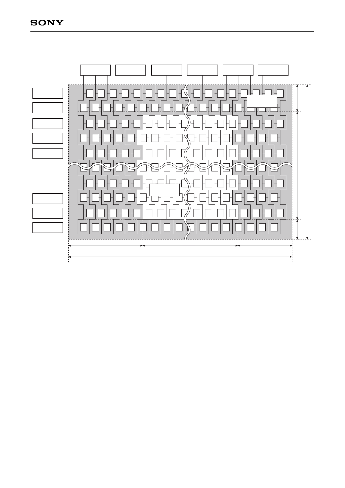
– 46 –
CXA3017R
LCX027AK/AKB Pixel Arrangement
B R G B R G B R G B R G B R G B R
GRBGRBGRBGRBGRBGR
B R G B R G B R G B R G B R G B R
GRBGRBGRBGRBGRBGR
B R G B R G B R G B R G B R G B R
GRBGRBGRBGRBGRBGR
B R G B R G B R G B R G B R G B R
GRBGRBGRBGRBGRBGR
B R G B R G B R G B R G B R G B R
RBGRBGRBGRBGRBGR
G
Active area
2
1
225
228
HSW266 HSW268
dummy5 to 8
HSW3HSW1
dummy1 to 4
dummy1
Vline1
Vline2
Vline3
Vline224
Vline225
dummy3
dummy2
Photo-shielding
area
14 800 13
827
Page 47
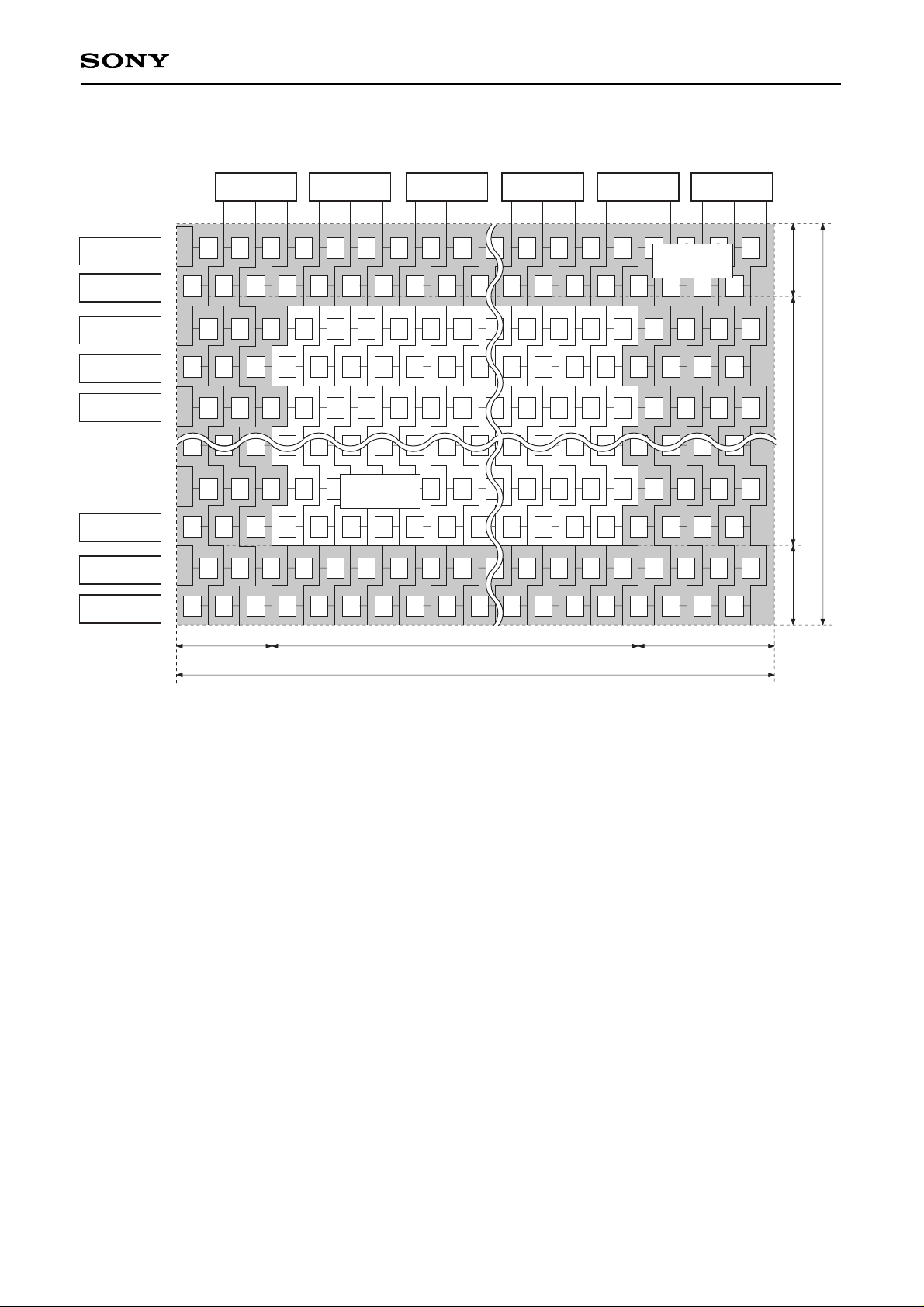
– 47 –
CXA3017R
LCX024AK/AKB Pixel Arrangement
B R G B R G B R G B R G B R G B R
GRBGRBGRBGRBGRBGR
B R G B R G B R G B R G B R G B R
GRBGRBGRBGRBGRBGR
B R G B R G B R G B R G B R G B R
GRBGRBGRBGRBGRBGR
B R G B R G B R G B R G B R G B R
GRBGRBGRBGRBGRBGR
B R G B R G B R G B R G B R G B R
RBGRBGRBGRBGRBGR
G
2
2
218
228
G
B
G
B
G
B
G
B
G
B
HSW176 HSW178 HSW179HSW3HSW2HSW1
dummy2
Vline1
Vline2
Vline3
Vline218
dummy3
dummy4
dummy1
Active area
Photo-shielding
area
537
3 521 13
Page 48
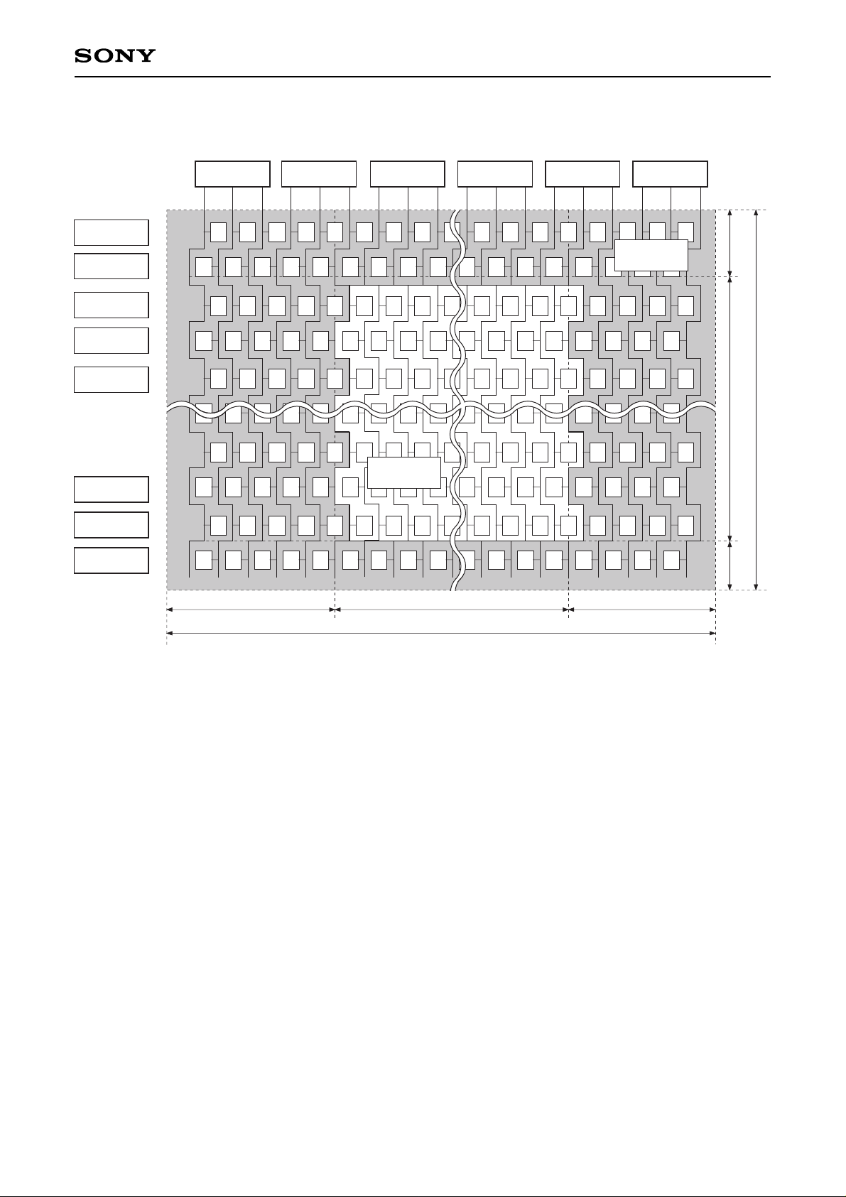
– 48 –
CXA3017R
LCX009AK/AKB Pixel Arrangement
B R G B R G B R G B R G B R G B R
GRBGRBGRBGRBGRBGR
B R G B R G B R G B R G B R G B R
GRBGRBGRBGRBGRBGR
B R G
B
R G B
R G B R
G B R G B R
GRBGRB
GRB
GRBGRBGR
B R G B R G B R G B R G B R G B R
GRBGRBGRBGRBGRBGR
B R G
B R G B R G B R G B R G B R
RBGRBGRBGRBGRBGR
G
2
1
225
228
HSW267 HSW268
dummy5 to 8
HSW2HSW1
dummy1 to 4
dummy2
Vline1
Vline2
Vline3
Vline224
Vline225
dummy3
dummy1
Active area
Photo-shielding
area
14 800 13
827
Page 49
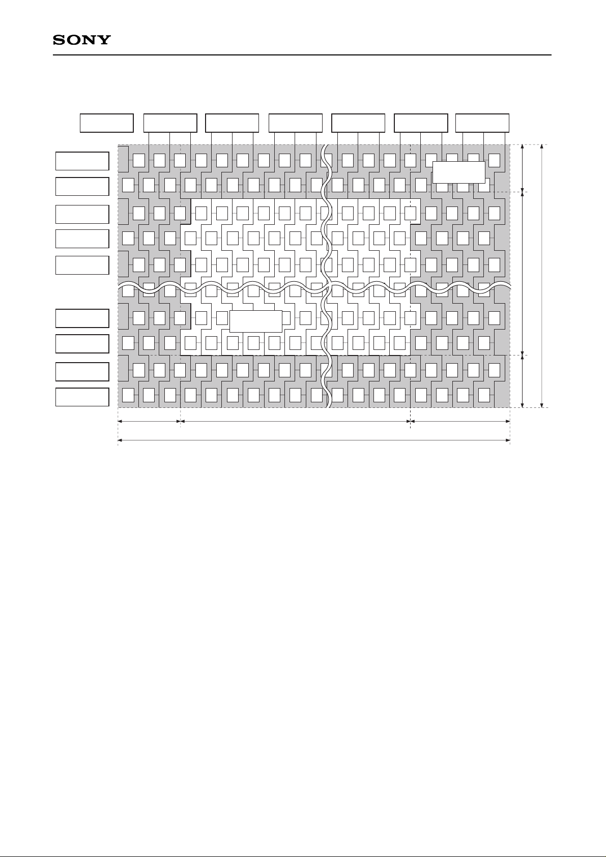
– 49 –
CXA3017R
LCX005BK/BKB Pixel Arrangement
B R G B R G B R G B R G B R G B R
GRBGRBGRBGRBGRBGR
B R G B R G B R G B R G B R G B R
GRBGRBGRBGRBGRBGR
B R G B R G B R G B R G B R G B R
GRBGRBGRBGRBGRBGR
B R G B R G B R G B R G B R G B R
GRBGRBGRBGRBGRBGR
B R G B R G B R G B R G B R G B R
RBGRBGRBGRBGRBGR
G
3 521 13
2
2
218
222
G
B
G
B
G
B
G
B
G
B
HSW174 HSW175
dummy2 to 5
HSW3HSW2HSW1
dummy2
Vline1
Vline2
Vline3
Vline217
Vline218
dummy3
dummy4
dummy1
Active area
Photo-shielding
area
dummy1
537
Page 50

– 50 –
CXA3017R
(MCK)
(SYNC)
(BLK)
HD
HST1
HCK1
SH3 (Internal)
SH4 (Internal)
SH2 (Internal)
FRP (Internal)
VCK1
VST/VD
EN1
EN2 (PAL)
HCK2
SH1 (Internal)
VCK2
EN1 (PAL)
VCK3
VCK4
PCG
CLR
HST2
4.7µs (53fH)
2.0µs (22fH) 4.5µs (50fH)
4.7µs (53fH)
3.0µs (34fH)
3.0µs (34fH)
0.5µs (6fH)
5.0µs (56fH)
22.5fH
13fH
5.0µs (56.5fH)
6.0µs (67.5fH)
3.0µs (34fH)
6.5µs (73fH)
Horizontal Direction Timing Chart — NTSC/PAL
LCX005 + (DCX501), LCX024 + (DCX501)
RGT1 = 0, RGT2 = 0, HP = 10000, HD = 00000
Cycle value NTSC: 690 ck, PAL: 716 ck
Note) The first (MCK), second (SYNC) and third (BLK) rows of the timing chart are pulses indicated as a reference and are not pulses output from pins.
FRP polarity is not specified for each line and field.
LCX005/024 drive pulses: HST2, HCK1, HCK2, EN2, CLR, VCK3, VCK4, VST(EN2 is high during NTSC.)
DCX501 drive pulses: HST1, HCK1, HCK2, VCK1, VCK2, PCG, EN1 and VST (HST1, PCG, EN1 and VST output inverted pulses XHST1, XPCG, XEN1 and XVST.)
ODD LINE
Page 51

– 51 –
CXA3017R
(MCK)
(SYNC)
(BLK)
HD
HST1
HCK1
SH3 (Internal)
SH4 (Internal)
SH2 (Internal)
FRP (Internal)
VCK1
VST/VD
EN1
EN2 (PAL)
HCK2
SH1 (Internal)
VCK2
EN1 (PAL)
VCK3
VCK4
PCG
CLR
HST2
4.7µs (53fH)
2.0µs (22fH) 4.5µs (50fH)
4.7µs (53fH)
3.0µs (34fH)
3.0µs (34fH)
0.5µs (6fH)
5.0µs (56fH)
21fH
13fH
6.0µs (66fH)
5.0µs (55fH)
6.5µs (73fH)
3.0µs (34fH)
Horizontal Direction Timing Chart — NTSC/PAL
LCX005 + (DCX501), LCX024 + (DCX501)
RGT1 = 0, RGT2 = 0, HP = 10000, HD = 00000
Cycle value NTSC: 690 ck, PAL: 716 ck
Note) The first (MCK), second (SYNC) and third (BLK) rows of the timing chart are pulses indicated as a reference and are not pulses output from pins.
FRP polarity is not specified for each line and field.
LCX005/024 drive pulses: HST2, HCK1, HCK2, EN2, CLR, VCK3, VCK4 and VST (EN2 is high during NTSC.)
DCX501 drive pulses: HST1, HCK1, HCK2, VCK1, VCK2, PCG, EN1 and VST (HST1, PCG, EN1 and VST output inverted pulses XHST1, XPCG, XEN1 and XVST.)
EVEN LINE
Page 52

– 52 –
CXA3017R
(MCK)
(SYNC)
(BLK)
HD
HST1
HCK1
HCK2
HST2
HST1
HCK1
HCK2
HST2
HST1
HCK1
HCK2
HST2
HST1
HCK1
HCK2
HST2
RGT1 = 0 or 1, RGT2 = 1
RGT1 = 0 or 1, RGT2 = 1
RGT1 = 0 or 1, RGT2 = 0
RGT1 = 0 or 1, RGT2 = 0
EVEN LINE
ODD LINE
EVEN LINE
ODD LINE
4.7µs (53fH)
2.0µs (22fH) 4.5µs (50fH)
4.7µs (53fH)
13fH
13fH
13fH
13fH
22.5fH
21fH
22fH
23.5fH
Horizontal Direction Timing Chart — NTSC/PAL
LCX005 + (DCX501), LCX024 + (DCX501)
HST1 and HST2 during right/left inversion
Note) The first (MCK), second (SYNC) and third (BLK) rows of the timing chart are pulses indicated as a reference and are not pulses output from pins.
HST1: DCX501 horizontal display start pulse (inverted pulse XHST1 output)
HST2: LCX005/024 horizontal display start pulse
Page 53
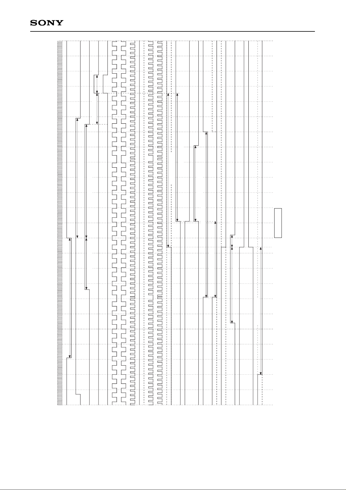
– 53 –
CXA3017R
(MCK)
(SYNC)
(BLK)
HD
HST1
HCK1
SH3 (Internal)
SH4 (Internal)
SH2 (Internal)
FRP (Internal)
VCK1
VST/VD
EN1
EN2 (PAL)
HCK2
SH1 (Internal)
VCK2
EN1 (PAL)
VCK3, (4)
VCK4, (3)
PCG
CLR
HST2
6.5µs (109fH)
3.0µs (50fH)
3.0µs (50fH)
3.0µs (50fH)
0.5µs (8fH)
5.0µs (84fH)
6.0µs (101.5fH)
5.0µs (84.5fH)
20.5fH
4.7µs (79fH)
12fH
4.5µs (75fH)
4.7µs (79fH)
2.0µs (34fH)
Horizontal Direction Timing Chart — NTSC/PAL
LCX009 + (DCX501), LCX027 + (DCX501)
DCX501 + (LCX009), DCX501 + (LCX027), DCX501 + (LCX005), DCX501 + (LCX024)
RGT1 = 0, RGT2 = 0, HP = 10000, HD = 00000
Cycle value NTSC: 1034 ck, PAL: 1072 ck
Note) The first (MCK), second (SYNC) and third (BLK) rows of the timing chart are pulses indicated as a reference and are not pulses output from pins.
FRP polarity is not specified for each line and field.
In LCX009 + (DCX501) and DCX501 + (LCX009) modes, the VCK3 and VCK4 polarities are inverted. (VCK(3) and VCK(4))
LCX009/027, 005/024 drive pulses: HST2, HCK1, HCK2, EN2, CLR, VCK3, VCK4 and VST (EN2 is high during NTSC.)
DCX501 drive pulses: HST1, HCK1, HCK2, VCK1, VCK2, PCG, EN1 and VST (HST1, PCG, EN1 and VST output inverted pulses XHST1, XPCG, XEN1 and XVST.)
ODD LINE
Page 54

– 54 –
CXA3017R
(MCK)
(SYNC)
(BLK)
HD
HST1
HCK1
SH3 (Internal)
SH4 (Internal)
SH2 (Internal)
FRP (Internal)
VCK1
VST/VD
EN1
EN2 (PAL)
HCK2
SH1 (Internal)
VCK2
EN1 (PAL)
VCK3, (4)
VCK4, (3)
PCG
CLR
HST2
5.0µs (83fH)
19f
H
4.7µs (79fH)
2.0µs (34fH)
4.5µs (75fH)
4.7µs (79fH)
6.5µs (109fH)
3.0µs (50fH)
3.0µs (50fH)
3.0µs (50fH)
0.5µs (8fH)
5.0µs (84fH)
12fH
6.0µs (100fH)
Horizontal Direction Timing Chart — NTSC/PAL
LCX009 + (DCX501), LCX027 + (DCX501)
DCX501 + (LCX009), DCX501 + (LCX027), DCX501 + (LCX005), DCX501 + (LCX024)
RGT1 = 0, RGT2 = 0, HP = 10000, HD = 00000
Cycle value NTSC: 1034 ck, PAL: 1072 ck
Note) The first (MCK), second (SYNC) and third (BLK) rows of the timing chart are pulses indicated as a reference and are not pulses output from pins.
FRP polarity is not specified for each line and field.
In LCX009 + (DCX501) and DCX501 + (LCX009) modes, the VCK3 and VCK4 polarities are inverted. (VCK(3) and VCK(4))
LCX009/027, 005/024 drive pulses: HST2, HCK1, HCK2, EN2, CLR, VCK3, VCK4 and VST (EN2 is high during NTSC.)
DCX501 drive pulses: HST1, HCK1, HCK2, VCK1, VCK2, PCG, EN1 and VST (HST1, PCG, EN1 and VST output inverted pulses XHST1, XPCG, XEN1 and XVST.)
EVEN LINE
Page 55
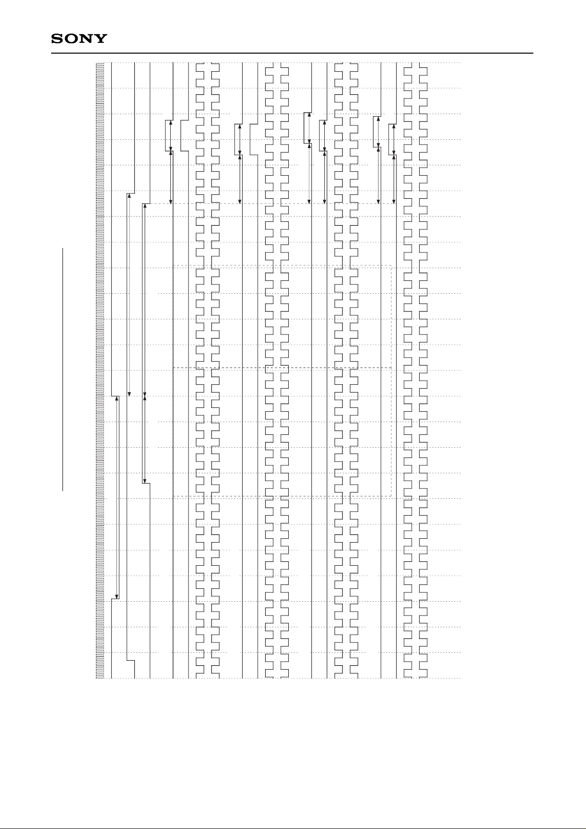
– 55 –
CXA3017R
(MCK)
(SYNC)
(BLK)
HD
HST1
HST2
HCK1
HCK2
HST1
HST2
HCK1
HCK2
HST1
HST2
HCK1
HCK2
HST1
HST2
HCK1
HCK2
20.5fH
12fH
12fH
19fH
23.5fH
12fH
12fH
20.5fH
22fH
12fH
12fH
19fH
4.7µs (79fH)
2.0µs (34fH)
4.5µs (75fH)
4.7µs (79fH)
ODD LINE
RGT1 = 0, RGT2 = 0
EVEN LINE
RGT1 = 0, RGT2 = 0
ODD LINE
RGT1 = 1, RGT2 = 0
EVEN LINE
RGT1 = 1, RGT2 = 0
Horizontal Direction Timing Chart — NTSC/PAL
LCX009 + (DCX501), LCX027 + (DCX501)
HST1 and HST2 during right/left inversion, RGT2 = 0
Note) The first (MCK), second (SYNC) and third (BLK) rows of the timing chart are pulses indicated as a reference and are not pulses output from pins.
HST1: DCX501 horizontal display start pulse (inverted pulse XHST1 output)
HST2: LCX009/027 horizontal display start pulse
Page 56

– 56 –
CXA3017R
(MCK)
(SYNC)
(BLK)
HD
HST1
HST2
HCK1
HCK2
HST1
HST2
HCK1
HCK2
HST1
HST2
HCK1
HCK2
HST1
HST2
HCK1
HCK2
4.7µs (79fH)
2.0µs (34fH)
4.7µs (79fH)
4.5µs (75fH)
23fH
12fH
12fH
20fH
24.5fH
12fH
12fH
21.5fH
12fH20fH
12fH21.5fH
ODD LINE
RGT1 = 0, RGT2 = 1
EVEN LINE
RGT1 = 0, RGT2 = 1
ODD LINE
RGT1 = 1, RGT2 = 1
EVEN LINE
RGT1 = 1, RGT2 = 1
Horizontal Direction Timing Chart — NTSC/PAL
LCX009 + (DCX501), LCX027 + (DCX501)
HST1 and HST2 during right/left inversion, RGT2 = 1
Note) The first (MCK), second (SYNC) and third (BLK) rows of the timing chart are pulses indicated as a reference and are not pulses output from pins.
HST1: DCX501 horizontal display start pulse (inverted pulse XHST1 output)
HST2: LCX009/027 horizontal display start pulse
Page 57

– 57 –
CXA3017R
(MCK)
(SYNC)
(BLK)
HD
HST1
HST2
HCK1
HCK2
HST1
HST2
HCK1
HCK2
HST1
HST2
HCK1
HCK2
HST1
HST2
HCK1
HCK2
2.0µs (34fH)
4.7µs (79fH)
4.7µs (79fH)
4.5µs (75fH)
20.5fH 12fH
19fH 12fH
20.5fH
12fH
12fH
19fH
12fH
22fH
12fH
23.5fH
ODD LINE
RGT1 = 0, RGT2 = 0
EVEN LINE
RGT1 = 0, RGT2 = 0
ODD LINE
RGT1 = 0, RGT2 = 1
EVEN LINE
RGT1 = 0, RGT2 = 1
Horizontal Direction Timing Chart — NTSC/PAL
DCX501 + (LCX009), DCX501 + (LCX027)
HST1 and HST2 during right/left inversion, RGT1 = 0
Note) The first (MCK), second (SYNC) and third (BLK) rows of the timing chart are pulses indicated as a reference and are not pulses output from pins.
HST1: DCX501 horizontal display start pulse (inverted pulse XHST1 output)
HST2: LCX009/027 horizontal display start pulse
Page 58

– 58 –
CXA3017R
(MCK)
(SYNC)
(BLK)
HD
HST1
HST2
HCK1
HCK2
HST1
HST2
HCK1
HCK2
HST1
HST2
HCK1
HCK2
HST1
HST2
HCK1
HCK2
4.7µs (79fH)
4.7µs (79fH)
4.5µs (75fH)2.0µs (34fH)
12fH
12fH
12fH
12fH
12fH
12fH
20fH
23fH
21.5fH
24.5fH
20fH
21.5fH
ODD LINE
RGT1 = 1, RGT2 = 0
EVEN LINE
RGT1 = 1, RGT2 = 0
ODD LINE
RGT1 = 1, RGT2 = 1
EVEN LINE
RGT1 = 1, RGT2 = 1
Horizontal Direction Timing Chart — NTSC/PAL
DCX501 + (LCX009), DCX501 + (LCX027)
HST1 and HST2 during right/left inversion, RGT1 = 1
Note) The first (MCK), second (SYNC) and third (BLK) rows of the timing chart are pulses indicated as a reference and are not pulses output from pins.
HST1: DCX501 horizontal display start pulse (inverted pulse XHST1 output)
HST2: LCX009/027 horizontal display start pulse
Page 59

– 59 –
CXA3017R
(MCK)
(SYNC)
(BLK)
HD
HST1
HST2
HCK1
HCK2
HST1
HST2
HCK1
HCK2
HST1
HST2
HCK1
HCK2
HST1
HST2
HCK1
HCK2
4.7µs (79fH)
2.0µs (34fH)
4.7µs (79fH)
4.5µs (75fH)
20.5f
H
19fH
20fH
12fH
23fH
21.5fH
12fH
24.5fH
12fH
12fH
12fH
12fH
ODD LINE
RGT1 = 0, RGT2 = 0 or 1
EVEN LINE
RGT1 = 0, RGT2 = 0 or1
ODD LINE
RGT1 = 1, RGT2 = 0 or 1
EVEN LINE
RGT1 = 1, RGT2 = 0 or 1
Horizontal Direction Timing Chart — NTSC/PAL
DCX501 + (LCX005), DCX501 + (LCX024)
HST1 and HST2 during right/left inversion
Note) The first (MCK), second (SYNC) and third (BLK) rows of the timing chart are pulses indicated as a reference and are not pulses output from pins.
HST1: DCX501 horizontal display start pulse (inverted pulse XHST1 output)
HST2: LCX005/024 horizontal display start pulse
Page 60

– 60 –
CXA3017R
(SYNC)
(BLK)
VD
VST
HD
HST1
HST2
VCK2, 3
VCK1, 4
FRP (Internal)
FRP (Internal)
1F inversion
PCG
EN1
EN2
CLR
BLK
SBLK
(Internal)
: Display start line
: Display end line
Vertical Direction Timing Chart — NTSC
LCX005 + (DCX501), LCX024 + (DCX501)
Note) The first (SYNC) and second (BLK) rows of the timing chart are pulses indicated as a reference and are not pulses output from pins.
FRP polarity is not specified for each line and field.
LCX005/024 drive pulses: HST2, EN2, CLR, VCK3, VCK4, VST and BLK
DCX501 drive pulses: VCK1, VCK2, HST1, EN1, PCG and VST (HST1, EN1, PCG and VST output inverted pulses XHST1, XEN1, XPCG and XVST.)
ODD FIELD
Page 61

– 61 –
CXA3017R
FRP (Internal)
1F inversion
(SYNC)
(BLK)
VD
VST
HD
HST1
HST2
VCK2, 3
VCK1, 4
FRP (Internal)
PCG
EN1
EN2
CLR
BLK
SBLK
(Internal)
: Display start line
: Display end line
Vertical Direction Timing Chart — NTSC
LCX005 + (DCX501), LCX024 + (DCX501)
Note) The first (SYNC) and second (BLK) rows of the timing chart are pulses indicated as a reference and are not pulses output from pins.
FRP polarity is not specified for each line and field.
LCX005/024 drive pulses: HST2, EN2, CLR, VCK3, VCK4, VST and BLK
DCX501 drive pulses: VCK1, VCK2, HST1, EN1, PCG and VST (HST1, EN1, PCG and VST output inverted pulses XHST1, XEN1, XPCG and XVST.)
EVEN FIELD
Page 62

– 62 –
CXA3017R
FRP (Internal)
1F inversion
(SYNC)
(BLK)
VD
VST
HD
HST1
HST2
VCK2, 3
VCK1, 4
FRP (Internal)
PCG
EN1
EN2
CLR
BLK
SBLK
(Internal)
: Display start line
: Display end line
Vertical Direction Timing Chart — PAL
LCX005 + (DCX501), LCX024 + (DCX501)
Note) The first (SYNC) and second (BLK) rows of the timing chart are pulses indicated as a reference and are not pulses output from pins.
FRP polarity is not specified for each line and field.
LCX005/024 drive pulses: HST2, EN2, CLR, VCK3, VCK4, VST and BLK
DCX501 drive pulses: VCK1, VCK2, HST1, EN1, PCG and VST (HST1, EN1, PCG and VST output inverted pulses XHST1, XEN1, XPCG and XVST.)
ODD FIELD
Page 63
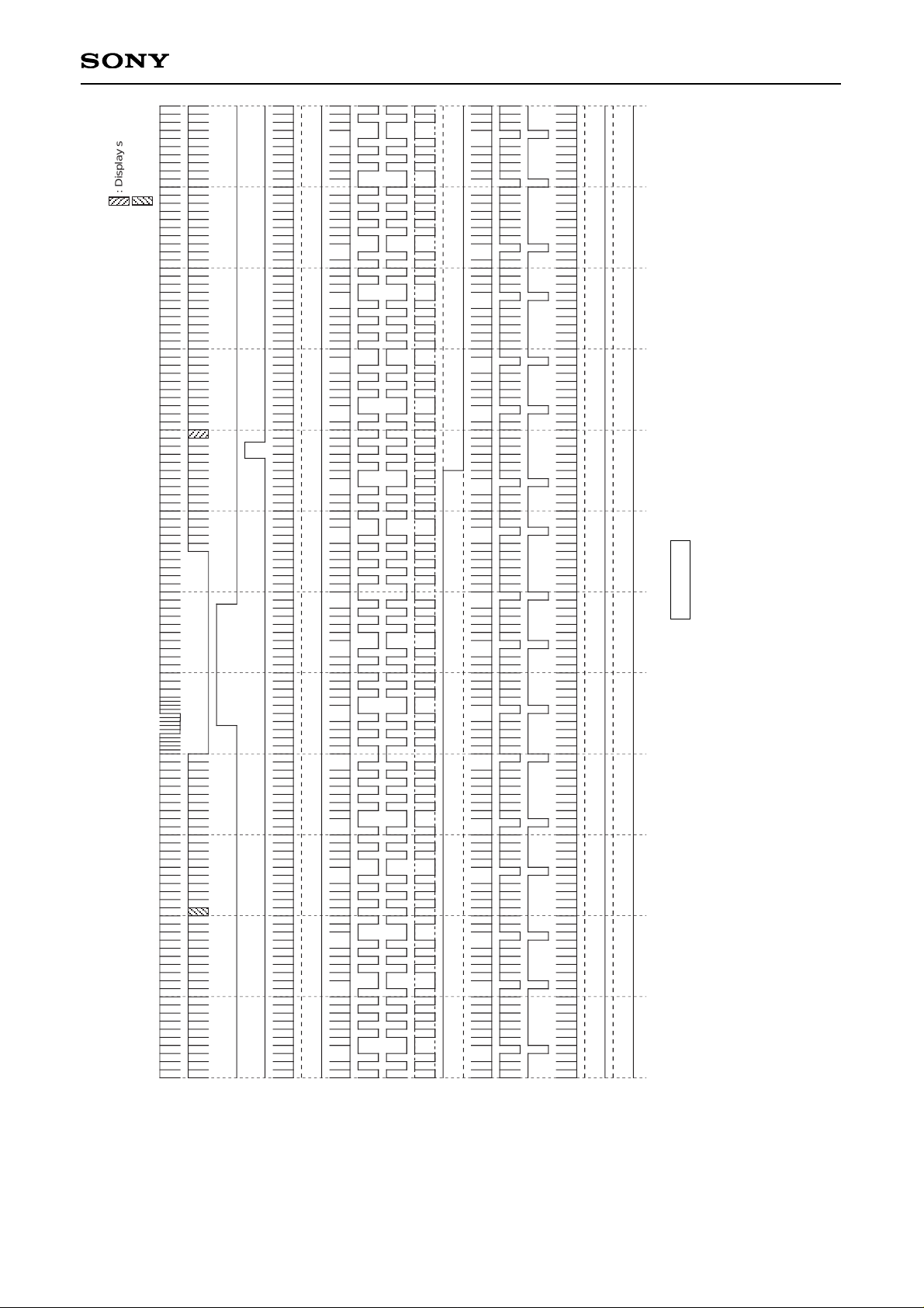
– 63 –
CXA3017R
FRP (Internal)
1F inversion
(SYNC)
(BLK)
VD
VST
HD
HST1
HST2
VCK2, 3
VCK1, 4
FRP (Internal)
PCG
EN1
EN2
CLR
BLK
SBLK
(Internal)
: Display start line
: Display end line
Vertical Direction Timing Chart — PAL
LCX005 + (DCX501), LCX024 + (DCX501)
Note) The first (SYNC) and second (BLK) rows of the timing chart are pulses indicated as a reference and are not pulses output from pins.
FRP polarity is not specified for each line and field.
LCX005/024 drive pulses: HST2, EN2, CLR, VCK3, VCK4, VST and BLK
DCX501 drive pulses: VCK1, VCK2, HST1, EN1, PCG and VST (HST1, EN1, PCG and VST output inverted pulses XHST1, XEN1, XPCG and XVST.)
EVEN FIELD
Page 64

– 64 –
CXA3017R
FRP (Internal)
1F inversion
(SYNC)
(BLK)
VD
VST
HD
HST1
HST2
VCK1, 4, (3)
VCK2, 3, (4)
FRP (Internal)
PCG
EN1
EN2
CLR
BLK
SBLK
(Internal)
: Display start line
: Display end line
Vertical Direction Timing Chart — NTSC
LCX009 + (DCX501), LCX027 + (DCX501), DCX501 + (LCX009), DCX501 + (LCX027),
DCX501 + (LCX005), DCX501 + (LCX024)
Note) The first (SYNC) and second (BLK) rows of the timing chart are pulses indicated as a reference and are not pulses output from pins.
FRP polarity is not specified for each line and field.
In LCX009 + (DCX501) and DCX501 + (LCX009) modes, the VCK3 and VCK4 polarities are inverted. (VCK(3) and VCK(4))
LCX009/027 drive pulses: HST2, EN2, CLR, VCK3, VCK4, VST and BLK
DCX501 drive pulses: VCK1, VCK2, HST1, EN1, PCG and VST (HST1, EN1, PCG and VST output inverted pulses XHST1, XEN1, XPCG and XVST.)
ODD FIELD
Page 65

– 65 –
CXA3017R
FRP (Internal)
1F inversion
(SYNC)
(BLK)
VD
VST
HD
HST1
HST2
VCK1, 4, (3)
VCK2, 3, (4)
FRP (Internal)
PCG
EN1
EN2
CLR
BLK
SBLK
(Internal)
: Display start line
: Display end line
Vertical Direction Timing Chart — NTSC
LCX009 + (DCX501), LCX027 + (DCX501), DCX501 + (LCX009), DCX501 + (LCX027),
DCX501 + (LCX005), DCX501 + (LCX024)
Note) The first (SYNC) and second (BLK) rows of the timing chart are pulses indicated as a reference and are not pulses output from pins.
FRP polarity is not specified for each line and field.
In LCX009 + (DCX501) and DCX501 + (LCX009) modes, the VCK3 and VCK4 polarities are inverted. (VCK(3) and VCK(4))
LCX009/027 drive pulses: HST2, EN2, CLR, VCK3, VCK4, VST and BLK
DCX501 drive pulses: VCK1, VCK2, HST1, EN1, PCG and VST (HST1, EN1, PCG and VST output inverted pulses XHST1, XEN1, XPCG and XVST.)
EVEN FIELD
Page 66

– 66 –
CXA3017R
FRP (Internal)
1F inversion
(SYNC)
(BLK)
VD
VST
HD
HST1
HST2
VCK1, 4, (3)
VCK2, 3, (4)
FRP (Internal)
PCG
EN1
EN2
CLR
BLK
SBLK
(Internal)
: Display start line
: Display end line
Vertical Direction Timing Chart — PAL
LCX009 + (DCX501), LCX027 + (DCX501), DCX501 + (LCX009), DCX501 + (LCX027),
DCX501 + (LCX005), DCX501 + (LCX024)
Note) The first (SYNC) and second (BLK) rows of the timing chart are pulses indicated as a reference and are not pulses output from pins.
FRP polarity is not specified for each line and field.
In LCX009 + (DCX501) and DCX501 + (LCX009) modes, the VCK3 and VCK4 polarities are inverted. (VCK(3) and VCK(4))
LCX009/027 drive pulses: HST2, EN2, CLR, VCK3, VCK4, VST and BLK
DCX501 drive pulses: VCK1, VCK2, HST1, EN1, PCG and VST (HST1, EN1, PCG and VST output inverted pulses XHST1, XEN1, XPCG and XVST.)
ODD FIELD
Page 67

– 67 –
CXA3017R
FRP (Internal)
1F inversion
(SYNC)
(BLK)
VD
VST
HD
HST1
HST2
VCK1, 4, (3)
VCK2, 3, (4)
FRP (Internal)
PCG
EN1
EN2
CLR
BLK
SBLK
(Internal)
: Display start line
: Display end line
Vertical Direction Timing Chart — PAL
LCX009 + (DCX501), LCX027 + (DCX501), DCX501 + (LCX009), DCX501 + (LCX027),
DCX501 + (LCX005), DCX501 + (LCX024)
Note) The first (SYNC) and second (BLK) rows of the timing chart are pulses indicated as a reference and are not pulses output from pins.
FRP polarity is not specified for each line and field.
In LCX009 + (DCX501) and DCX501 + (LCX009) modes, the VCK3 and VCK4 polarities are inverted. (VCK(3) and VCK(4))
LCX009/027 drive pulses: HST2, EN2, CLR, VCK3, VCK4, VST and BLK
DCX501 drive pulses: VCK1, VCK2, HST1, EN1, PCG and VST (HST1, EN1, PCG and VST output inverted pulses XHST1, XEN1, XPCG and XVST.)
EVEN FIELD
Page 68
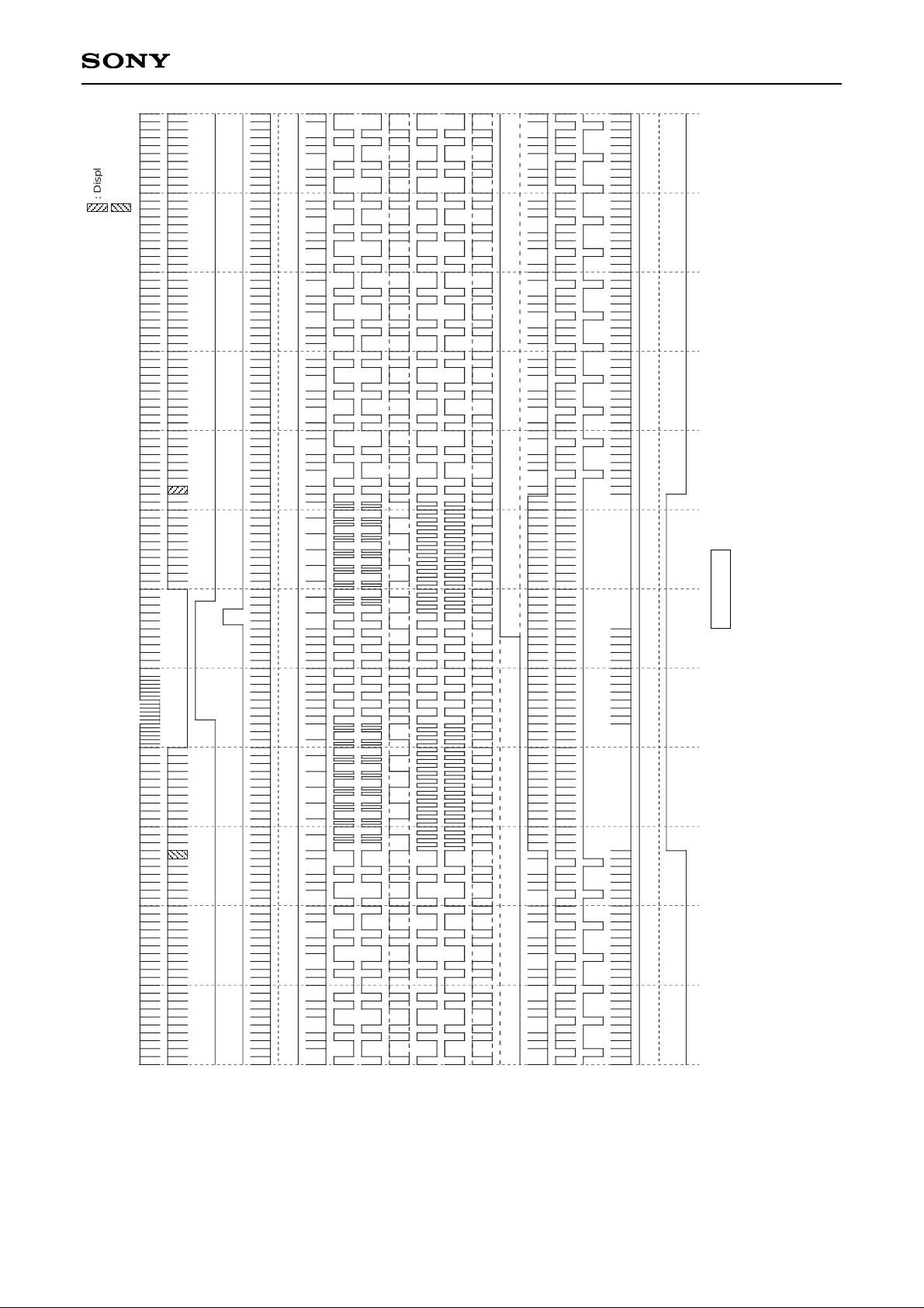
– 68 –
CXA3017R
FRP (Internal)
1F inversion
SBLK
(Internal)
(SYNC)
(BLK)
VD
VST
HD
HST1
HST2
VCK2, 3 (A)
VCK1, 4 (A)
FRP (Internal) (B)
PCG
EN1
EN2
CLR
BLK
FRP (Internal) (A)
VCK2, 3 (B)
VCK1, 4 (B)
: Display start line
: Display end line
Vertical Direction Timing Chart — NTSC-WIDE
LCX005 + (DCX501), LCX024 + (DCX501)
Note) The first (SYNC) and second (BLK) rows of the timing chart are pulses indicated as a reference and are not pulses output from pins.
FRP polarity is not specified for each line and field.
LCX005 + (DCX501) mode: VCK(A) output
LCX024 + (DCX501) mode: VCK(B) output
LCX005/024 drive pulses: HST2, EN2, CLR, VCK3, VCK4, VST and BLK
DCX501 drive pulses: VCK1, VCK2, HST1, EN1, PCG and VST (HST1, EN1, PCG and VST output inverted pulses XHST1, XEN1, XPCG and XVST.)
ODD FIELD
Page 69

– 69 –
CXA3017R
FRP (Internal)
1F inversion
SBLK
(Internal)
(SYNC)
(BLK)
VD
VST
HD
HST1
HST2
VCK2, 3 (A)
VCK1, 4 (A)
FRP (Internal) (B)
PCG
EN1
EN2
CLR
BLK
FRP (Internal) (A)
VCK2, 3 (B)
VCK1, 4 (B)
: Display start line
: Display end line
Vertical Direction Timing Chart — NTSC-WIDE
LCX005 + (DCX501), LCX024 + (DCX501)
Note) The first (SYNC) and second (BLK) rows of the timing chart are pulses indicated as a reference and are not pulses output from pins.
FRP polarity is not specified for each line and field.
LCX005 + (DCX501) mode: VCK(A) output
LCX024 + (DCX501) mode: VCK(B) output
LCX005/024 drive pulses: HST2, EN2, CLR, VCK3, VCK4, VST and BLK
DCX501 drive pulses: VCK1, VCK2, HST1, EN1, PCG and VST (HST1, EN1, PCG and VST output inverted pulses XHST1, XEN1, XPCG and XVST.)
EVEN FIELD
Page 70

– 70 –
CXA3017R
: Display start line
: Display end line
FRP (Internal)
1F inversion
SBLK
(Internal)
(SYNC)
(BLK)
VD
VST
HD
HST1
HST2
VCK2, 3 (A)
VCK1, 4 (A)
FRP (Internal) (B)
PCG
EN1
EN2
CLR
BLK
FRP (Internal) (A)
VCK2, 3 (B)
VCK1, 4 (B)
Vertical Direction Timing Chart — PAL-WIDE
LCX005 + (DCX501), LCX024 + (DCX501)
Note) The first (SYNC) and second (BLK) rows of the timing chart are pulses indicated as a reference and are not pulses output from pins.
FRP polarity is not specified for each line and field.
LCX005 + (DCX501) mode: VCK(A) output
LCX024 + (DCX501) mode: VCK(B) output
LCX005/024 drive pulses: HST2, EN2, CLR, VCK3, VCK4, VST and BLK
DCX501 drive pulses: VCK1, VCK2, HST1, EN1, PCG and VST (HST1, EN1, PCG and VST output inverted pulses XHST1, XEN1, XPCG and XVST.)
ODD FIELD
Page 71

– 71 –
CXA3017R
FRP (Internal)
1F inversion
SBLK
(Internal)
(SYNC)
(BLK)
VD
VST
HD
HST1
HST2
VCK2, 3 (A)
VCK1, 4 (A)
FRP (Internal) (B)
PCG
EN1
EN2
CLR
BLK
FRP (Internal) (A)
VCK2, 3 (B)
VCK1, 4 (B)
: Display start line
: Display end line
Vertical Direction Timing Chart — PAL-WIDE
LCX005 + (DCX501), LCX024 + (DCX501)
Note) The first (SYNC) and second (BLK) rows of the timing chart are pulses indicated as a reference and are not pulses output from pins.
FRP polarity is not specified for each line and field.
LCX005 + (DCX501) mode: VCK(A) output
LCX024 + (DCX501) mode: VCK(B) output
LCX005/024 drive pulses: HST2, EN2, CLR, VCK3, VCK4, VST and BLK
DCX501 drive pulses: VCK1, VCK2, HST1, EN1, PCG and VST (HST1, EN1, PCG and VST output inverted pulses XHST1, XEN1, XPCG and XVST.)
EVEN FIELD
Page 72
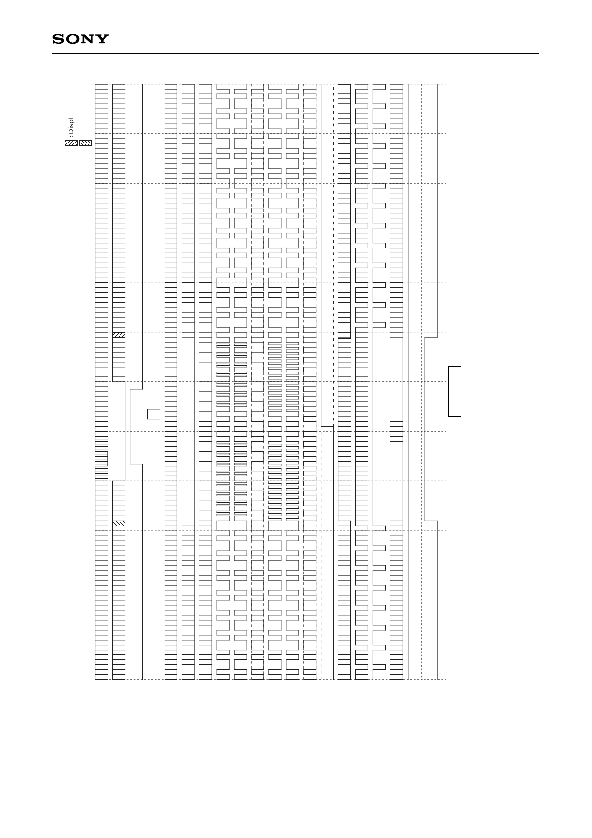
– 72 –
CXA3017R
FRP (Internal)
1F inversion
SBLK
(Internal)
(SYNC)
(BLK)
VD
VST
HD
HST1
HST2
VCK1, 3, (4) (A)
VCK2, 4, (3) (A)
FRP (Internal) (B)
PCG
EN1
EN2
CLR
BLK
FRP (Internal) (A)
VCK1, 4 (B)
VCK2, 3 (B)
: Display start line
: Display end line
Vertical Direction Timing Chart — NTSC-WIDE
LCX009 + (DCX501), LCX027 + (DCX501),
DCX501 + (LCX009), DCX501 + (LCX027), DCX501 + (LCX005)
Note) The first (SYNC) and second (BLK) rows of the timing chart are pulses indicated as a reference and are not pulses output from pins.
FRP polarity is not specified for each line and field.
LCX009 + (DCX501), DCX501 + (LCX009) and DCX501 + (LCX005) modes: VCK(A) output
(In DCX501 + (LCX005) mode the polarity is inverted. (VCK(3)(A) and VCK(4)(A)))
LCX027 + (DCX501) and DCX501 + (LCX027) modes: VCK(B) output
LCX009/027 drive pulses: HST2, EN2, CLR, VCK3, VCK4, VST and BLK
DCX501 drive pulses: VCK1, VCK2, HST1, EN1, PCG and VST (HST1, EN1, PCG and VST output inverted pulses XHST1, XEN1, XPCG and XVST.)
ODD FIELD
Page 73

– 73 –
CXA3017R
(SYNC)
(BLK)
VD
VST
HD
HST1
HST2
VCK1, 3, (4) (A)
VCK2, 4, (3) (A)
FRP (Internal) (B)
FRP (Internal)
1F inversion
PCG
EN1
EN2
CLR
BLK
SBLK
(Internal)
FRP (Internal) (A)
VCK1, 4 (B)
VCK2, 3 (B)
: Display start line
: Display end line
Vertical Direction Timing Chart — NTSC-WIDE
LCX009 + (DCX501), LCX027 + (DCX501),
DCX501 + (LCX009), DCX501 + (LCX027), DCX501 + (LCX005)
Note) The first (SYNC) and second (BLK) rows of the timing chart are pulses indicated as a reference and are not pulses output from pins.
FRP polarity is not specified for each line and field.
LCX009 + (DCX501), DCX501 + (LCX009) and DCX501 + (LCX005) modes: VCK(A) output
(In DCX501 + (LCX005) mode the polarity is inverted. (VCK(3)(A) and VCK(4)(A)))
LCX027 + (DCX501) and DCX501 + (LCX027) modes: VCK(B) output
LCX009/027 drive pulses: HST2, EN2, CLR, VCK3, VCK4, VST and BLK
DCX501 drive pulses: VCK1, VCK2, HST1, EN1, PCG and VST (HST1, EN1, PCG and VST output inverted pulses XHST1, XEN1, XPCG and XVST.)
EVEN FIELD
Page 74

– 74 –
CXA3017R
FRP (Internal)
1F inversion
SBLK
(Internal)
(SYNC)
(BLK)
VD
VST
HD
HST1
HST2
VCK1, 3, (4) (A)
VCK2, 4, (3) (A)
FRP (Internal) (B)
PCG
EN1
EN2
CLR
BLK
FRP (Internal) (A)
VCK1, 4 (B)
VCK2, 3 (B)
: Display start line
: Display end line
Vertical Direction Timing Chart — PAL-WIDE
LCX009 + (DCX501), LCX027 + (DCX501),
DCX501 + (LCX009), DCX501 + (LCX027), DCX501 + (LCX005)
Note) The first (SYNC) and second (BLK) rows of the timing chart are pulses indicated as a reference and are not pulses output from pins.
FRP polarity is not specified for each line and field.
LCX009 + (DCX501), DCX501 + (LCX009) and DCX501 + (LCX005) modes: VCK(A) output
(In DCX501 + (LCX005) mode the polarity is inverted. (VCK(3)(A) and VCK(4)(A)))
LCX027 + (DCX501) and DCX501 + (LCX027) modes: VCK(B) output
LCX009/027 drive pulses: HST2, EN2, CLR, VCK3, VCK4, VST and BLK
DCX501 drive pulses: VCK1, VCK2, HST1, EN1, PCG and VST (HST1, EN1, PCG and VST output inverted pulses XHST1, XEN1, XPCG and XVST.)
ODD FIELD
Page 75

– 75 –
CXA3017R
(SYNC)
(BLK)
VD
VST
HD
HST1
HST2
VCK1, 3, (4) (A)
VCK2, 4, (3) (A)
FRP (Internal) (B)
FRP (Internal)
1F inversion
PCG
EN1
EN2
CLR
BLK
SBLK
(Internal)
FRP (Internal) (A)
VCK1, 4 (B)
VCK2, 3 (B)
: Display start line
: Display end line
Vertical Direction Timing Chart — PAL-WIDE
LCX009 + (DCX501), LCX027 + (DCX501),
DCX501 + (LCX009), DCX501 + (LCX027), DCX501 + (LCX005)
Note) The first (SYNC) and second (BLK) rows of the timing chart are pulses indicated as a reference and are not pulses output from pins.
FRP polarity is not specified for each line and field.
LCX009 + (DCX501), DCX501 + (LCX009) and DCX501 + (LCX005) modes: VCK(A) output
(In DCX501 + (LCX005) mode the polarity is inverted. (VCK(3)(A) and VCK(4)(A)))
LCX027 + (DCX501) and DCX501 + (LCX027) modes: VCK(B) output
LCX009/027 drive pulses: HST2, EN2, CLR, VCK3, VCK4, VST and BLK
DCX501 drive pulses: VCK1, VCK2, HST1, EN1, PCG and VST (HST1, EN1, PCG and VST output inverted pulses XHST1, XEN1, XPCG and XVST.)
EVEN FIELD
Page 76
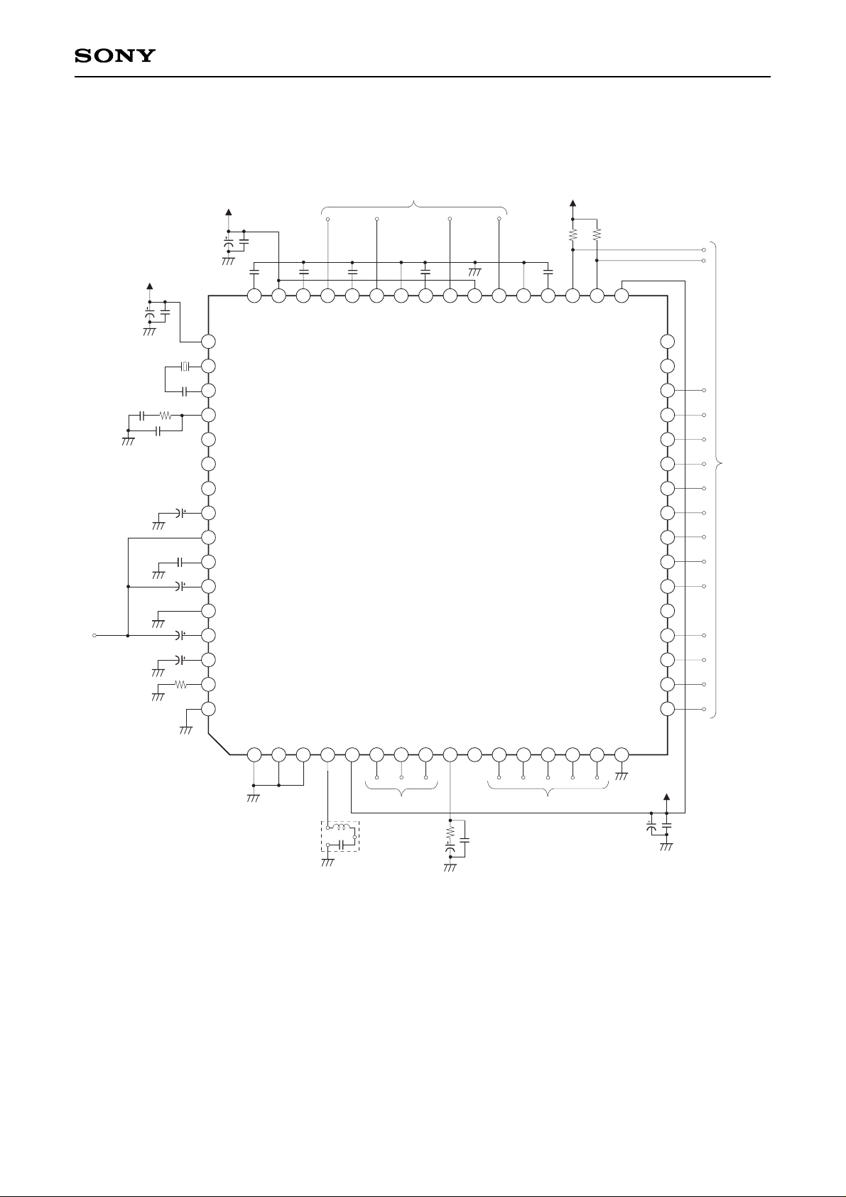
– 76 –
CXA3017R
Application Circuit (NTSC/PAL, COMP input)
To LCD panel
+3V
47µ
0.01µ
+12V
0.01µ
47µ 0.01µ
4
5
6
7
8
9
10
11
12
13
14
15
16
46
40
39
38
37
36
35
34
33
41
42
43
44
45
47
48
49
50
51
52
53
54
55
56
57
58
59
60
63
64
61
62
17
18
19
20
21
22
23
24
25
26
27
28
29
30
31
32
16p
0.33µ
V
CC1
VXO IN
APC
B-Y IN
R-Y IN
C OUT
V REG
C IN
RESET
Y IN
TEST2
SYNC IN
VSEP TC
F0 ADJ
GND1
DA OUT
VD
EN2
EN1
XEN1
VCK1
VCK2
VCK3
VCK4
VST
XVST
HD
PCG
XPCG
HCK1
HCK2
V
SS
XHST1
HST1
HST2
CLR
BLK
SCLK
DATA
LOAD
V
DD
1
TRAP
EXT B
EXT G
EXT R
V
DD
2
DWN
RGT1
FB PSIG
GND3
PSIG
V
CC
3
B OUT
FB B
GND2
FB G
R OUT
FB R
V
CC
2
SIG.CENTER
VXO OUT
RPD
TEST1
G OUT
10k
3.3µ
6800p
VDD of connected LCD panel
+15.5V
100k
100k
47µ
0.01µ
+3V
∗
2
15k
0.01µ
1µ
1µ
COMP IN
∗
1
0.22µ
0.033µ
10k
0.1µ
0.47µ 0.47µ
0.47µ
0.47µ
To LCD panel
To LCD panel
From serial controller
∗
3
2
3
1
∗1
Used crystal: KINSEKI CX-5F
Frequency deviation: within ±30ppm,
frequency temperature characteristics: within ±30ppm,
load capacity: 16pF
NTSC: 3.579545MHz
PAL: 4.433619MHz
∗2
Resistance value variation: ±2%,
temperature coefficient: ±200ppm or less
∗3
Trap (TDK)
NTSC: NLT4532-S3R6B
PAL: NLT4532-S4R4
Application circuits shown are typical examples illustrating the operation of the devices. Sony cannot assume responsibility for
any problems arising out of the use of these circuits or for any infringement of third party patent and other right due to same.
Page 77

– 77 –
CXA3017R
Application Circuit (NTSC/PAL, Y/C input)
+3V
47µ
0.01µ
+12V
0.01µ
47µ 0.01µ
2
4
5
6
7
8
9
10
11
12
13
14 15
16
46
40
39
38
37
36
35
34
33
41
42
43
44
45
47
48
49
50
51
52
53
54
55
56
57
58
59
60
63
64
61
62
17
18
19
20
21
22
23
24
25
26
27
28
29
30
31
32
16p
0.33µ
V
CC1
VXO IN
APC
B-Y IN
R-Y IN
C OUT
V REG
C IN
RESET
Y IN
TEST2
SYNC IN
VSEP TC
F0 ADJ
GND1
DA OUT
VD
EN2
EN1
XEN1
VCK1
VCK2
VCK3
VCK4
VST
XVST
HD
PCG
XPCG
HCK1
HCK2
V
SS
XHST1
HST1
HST2
CLR
BLK
SCLK
DATA
LOAD
V
DD
1
TRAP
EXT B
EXT G
EXT R
V
DD
2
DWN
RGT1
FB PSIG
GND3
PSIG
V
CC
3
B OUT
FB B
GND2
FB G
R OUT
FB R
V
CC
2
SIG.CENTER
VXO OUT
RPD
TEST1
G OUT
10k
3.3µ
6800p
VDD of connected LCD panel
+15.5V
100k
100k
47µ
0.01µ
+3V
0.01µ
1µ
1µ
Y IN
∗
1
0.22µ
0.033µ
10k
0.1µ
To LCD panel
0.47µ 0.47µ
0.47µ
0.47µ
To LCD panel
To LCD panel
From serial controller
C IN
3
1
∗1
Used crystal: KINSEKI CX-5F
Frequency deviation: within ±30ppm,
frequency temperature characteristics: within ±30ppm,
load capacity: 16pF
NTSC: 3.579545MHz
PAL: 4.433619MHz
Application circuits shown are typical examples illustrating the operation of the devices. Sony cannot assume responsibility for
any problems arising out of the use of these circuits or for any infringement of third party patent and other right due to same.
Page 78

– 78 –
CXA3017R
Application Circuit (NTSC/PAL, Y/color difference input)
+3V
47µ
0.01µ
+12V
0.01µ
47µ 0.01µ
2
4
5
6
7
8
9
10
11
12
13
14
15
16
46
40
39
38
37
36
35
34
33
41
42
43
44
45
47
48
49
50
51
52
53
54
55
56
57
58
59
60
63
64
61
62
17
18
19
20
21
22
23
24
25
26
27
28
29
30
31
32
0.33µ
V
CC1
VXO IN
APC
B-Y IN
R-Y IN
C OUT
V REG
C IN
RESET
Y IN
TEST2
SYNC IN
VSEP TC
F0 ADJ
GND1
DA OUT
VD
EN2
EN1
XEN1
VCK1
VCK2
VCK3
VCK4
VST
XVST
HD
PCG
XPCG
HCK1
HCK2
V
SS
XHST1
HST1
HST2
CLR
BLK
SCLK
DATA
LOAD
V
DD
1
TRAP
EXT B
EXT G
EXT R
V
DD
2
DWN
RGT1
FB PSIG
GND3
PSIG
V
CC
3
B OUT
FB B
GND2
FB G
R OUT
FB R
V
CC
2
SIG.CENTER
VXO OUT
RPD
TEST1
G OUT
10k
3.3µ
6800p
VDD of connected LCD panel
+15.5V
100k
100k
47µ
0.01µ
+3V
0.01µ
1µ
1µ
COMP/Y IN
To LCD panel
0.47µ 0.47µ
0.47µ
0.47µ
To LCD panel
To LCD panel
From serial controller
0.1µ
0.1µ
0.1µ
R-Y IN
B-Y IN
3
1
Application circuits shown are typical examples illustrating the operation of the devices. Sony cannot assume responsibility for
any problems arising out of the use of these circuits or for any infringement of third party patent and other right due to same.
Page 79

– 79 –
CXA3017R
Example of Representative Characteristics
1600
DAC value
HUE adjustment characteristics
HUE adjustment angle [deg]
–30
0
30
45
–60
256
–45
–15
15
32 64 96 224128 192
1600
DAC value
COLOR adjustment characteristics
Gain [dB]
–20.00
0.00
10.00
–40.00
256
–30.00
–10.00
32 64 96 224128 192
1600
DAC value
CONTRAST adjustment characteristics
Output gain [dB]
–10.00
5.00
10.00
–25.00
256
–15.00
–5.00
32 64 96 224128 192
0.00
–20.00
1600
DAC value
SUB-BRIGHT adjustment characteristics
Voltage change with respect to G output [V]
–1
0.5
1.5
2
–2
256
0
1
32 64 96 224128 192
–0.5
–1.5
1600
DAC value
Black limiter control characteristics
Limiter voltage [Vp-p]
8
10
11
6
256
7
9
32 64 96 224128 192
1600
DAC value
BRIGHT adjustment characteristics
Non-inverted output black level [V]
2
5
7
8
–2
256
0
4
6
32 64 96 224128 192
3
–1
1
Inverted output black level [V]
8
11
13
14
4
6
10
12
9
5
7
Non-inverted black
Inverted black
Page 80

– 80 –
CXA3017R
1600
DAC value
PSIG adjustment characteristics
Output amplitude [Vp-p]
4
8
10
0
256
2
6
32 64 96 224128 192
1600
DAC value
SUB-CONTRAST adjustment characteristics (γ1 = γ2 = 0)
Gain [dB]
–1.00
2.00
4.00
–4.00
256
–2.00
0.00
32 64 96 224128 192
–3.00
1.00
3.00
50
DAC value
DA OUT output adjustment characteristics
Output voltage [V]
1.5
2.5
3
0
7
1
2
1 2 3 4 6
0.5
1600
DAC value
Color difference balance adjustment
Gain [dB]
–1.00
3.00
5.00
–5.00
256
–3.00
1.00
32 64 96 224128 192
B-Y output [dB]
R-Y output [dB]
1600
DAC value
USER-BRIGHT adjustment characteristics
Non-inverted output black level [V]
2
5
7
8
–2
256
0
4
6
32 64 96 224128 192
3
–1
1
Inverted output black level [V]
8
11
13
14
4
6
10
12
9
5
7
Non-inverted black
Inverted black
Page 81

– 81 –
CXA3017R
0
Frequency [MHz]
Sharpness characteristics (γ1 = γ2 = 0)
Gain [dB]
–15.00
0.00
10.00
–30.00
12
–20.00
–10.00
2 4 6 108
–25.00
–5.00
5.00
(COMP, PAL, 009AK/AKB)
DAC = 0
DAC = 128
DAC = 255
0
Frequency [MHz]
Sharpness characteristics (γ1 = γ2 = 0)
Gain [dB]
–5.00
10.00
20.00
–15.00
12
–10.00
0.00
2 4 6 108
5.00
15.00
0
Frequency [MHz]
Sharpness characteristics (γ1 = γ2 = 0)
Gain [dB]
–5.00
10.00
15.00
–15.00
12
–10.00
0.00
2 4 6 108
5.00
0
Frequency [MHz]
Sharpness characteristics (γ1 = γ2 = 0)
Gain [dB]
–15.00
0.00
15.00
–30.00
12
–20.00
–10.00
2 4 6 10
8
–25.00
–5.00
5.00
10.00
0
Frequency [MHz]
Sharpness characteristics (γ1 = γ2 = 0)
Gain [dB]
–15.00
0.00
15.00
–30.00
12
–20.00
–10.00
2 4 6 108
–25.00
–5.00
5.00
10.00
0
Frequency [MHz]
Sharpness characteristics (γ1 = γ2 = 0)
Gain [dB]
–15.00
0.00
10.00
–30.00
12
–20.00
–10.00
2 4 6 108
–25.00
–5.00
5.00
(Y/C, 009AK/AKB)
DAC = 0
DAC = 128
DAC = 255
(Y/C, 005BK/BKB)
DAC = 0
DAC = 128
DAC = 255
(COMP, NTSC, 009AK/AKB)
DAC = 0
DAC = 128
DAC = 255
(COMP, NTSC, 005BK/BKB)
DAC = 0
DAC = 128
DAC = 255
(COMP, PAL, 005BK/BKB)
DAC = 0
DAC = 128
DAC = 255
Page 82

– 82 –
CXA3017R
Notes on Operation
The CXA3017R contains digital circuits, so the set board pattern must be designed in consideration of undesired
radiation, interference to analog circuits, etc. Care should also be taken for the following items when designing
the pattern.
• Make the IC power supply and GND patterns as plain as possible. In particular, GND and Vss should not
be separated and should be connected to the same GND pattern as close to the pins as possible.
• Connect the by-pass capacitors between the power supplies and GND as close to the pins as possible.
• The trap connected to Pin 4 should be located as close to the pin as possible. Also, do not pass other
signal lines close to this pin or the connected trap.
• The wiring for the crystal and capacitor connected to Pins 50 and 51 should be as short as possible in
order to prevent floating capacitance. Do not pass other signal lines close to these pins and wiring in order
to prevent interference such as color unevenness. In addition, the APC pull-in characteristics vary
significantly according to the characteristics of the used crystal and the wiring pattern, so be sure to
thoroughly investigate these items before using the set.
• The resistor connected to Pin 63 should be located as close to the pin as possible. Also, do not pass other
signal lines close to this pin.
The composite/Y signal and the external R-Y and B-Y signals are clamped at the inputs using the capacitors
connected to the input pins, so these signals should be input at sufficiently low impedance. The C signal is
received by the internal capacitor, so this signal should be input at low impedance after applying an
appropriate external DC bias.
The smoothing capacitor of the DC level control feedback circuit in the output block should have a leak current
with a small absolute value and variance.
A thorough study of the external buffer for PSIG output should be made before deciding on a circuit to
ascertain that it sufficiently brings out the characteristics of the LCD panel.
If this IC is used in connection with a circuit other than an LCD, it may cause that circuit to malfunction
depending on the order in which power is supplied to the circuits. Thoroughly study the consequences of using
this IC with other circuits before deciding on its use.
Since this IC utilizes a C-MOS structure, it may latch up due to excessive noise or power surge greater than
the maximum rating of the I/O pins, or due to interface with the power supply of another circuit, or due to the
order in which power is supplied to circuits. Be sure to take measures against the possibility of latch up.
Do not apply a voltage higher than VDD or lower than Vss to I/O pins.
Do not use this IC under operating conditions other than those given.
Absolute maximum rating values should not be exceeded even momentarily. Exceeding ratings may damage
the device, leading to eventual breakdown.
This IC has a MOS structure which is easily damaged by static electricity, so thorough measures should be
taken to prevent electrostatic discharge.
Page 83
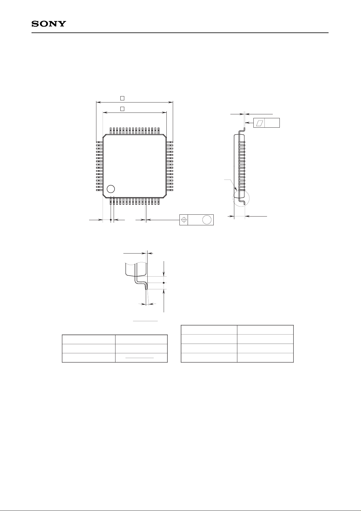
– 83 –
CXA3017R
Package Outline Unit: mm
SONY CODE
EIAJ CODE
JEDEC CODE
PACKAGE MATERIAL
LEAD TREATMENT
LEAD MATERIAL
PACKAGE WEIGHT
EPOXY RESIN
SOLDER PLATING
42 ALLOY
PACKAGE STRUCTURE
64PIN LQFP (PLASTIC)
12.0 ± 0.2
10.0 ± 0.2
48 33
1 16
49
64
32
17
1.25
0.5
+ 0.08
0.18 – 0.03
M
0.1
0.1 ± 0.1
(0.5)
0.5 ± 0.2
0° to 10°
1.7 MAX
DETAIL A
A
0.1
0.15 ± 0.05
LQFP-64P-L061
LQFP064-P-1010-AY
0.3g
 Loading...