

Page 1

—1—
E99866-TE
Sony reserves the right to change products and specifications without prior notice. This information does not convey any license by
any implication or otherwise under any patents or other right. Application circuits shown, if any, are typical examples illustrating the
operation of the devices. Sony cannot assume responsibility for any problems arising out of the use of these circuits.
Absolute Maximum Ratings (Ta=25 °C)
• Supply voltage VCC1, VCC2 –0.3 to +5.5 V
VCC3 –0.3 to +10.0 V
• Storage temperature Tstg –55 to +150 °C
• Allowable power dissipation
PD 580 mW
(when mounted on a printed circuit board)
Operating Conditions
• Supply voltage VCC1, VCC2 4.75 to 5.30 V
VCC3 4.75 to 9.45 V
• Operating temperature Topr –25 to +75 °C
Description
The CXA3250AN is a monolithic TV tuner IC which
integrates local oscillator and mixer circuits for VHF
band, local oscillator and mixer circuits for UHF
band, an IF amplifier and a tuning PLL onto a single
chip, enabling further miniaturization of the tuner.
Features
• Superior cross modulation
• Balanced UHF oscillator (4 pins) with excellent
oscillation stability
• Supports both I2C and 3-wire bus modes
• Automatic identification of 18, 19 or 27-bit control
(during 3-wire bus mode)
• On-chip A/D converter (during I2C bus mode)
• On-chip high voltage drive transistor for charge
pump
• Reference frequency selectable from 31.25, 50 or
62.5 kHz (when using a 4 MHz crystal)
• Low-phase noise synthesizer
• On-chip 4-output band switch (supports output
voltages from 5 to 9 V)
Applications
• TV tuners
• VCR tuners
• CATV tuners
Structure
Bipolar silicon monolithic IC
All Band TV Tuner IC with On-chip PLL
30 pin SSOP (Plastic)
CXA3250AN
This IC has the pins whose electrostatic discharge strength is weak as the operating frequency is high and the high-frequency
process is used for this IC.
Take care of handling the IC.
For the availability of this product, please contact the sales office.
Page 2
—2—
CXA3250AN
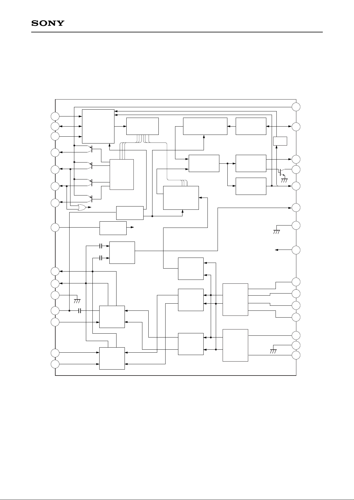
Block Diagram and Pin Configuration
Shift
Register
Programable
Divider
14/15bit
Divider
1/64, 80, 128
BUS
Interface
REF
OSC
Charge
Pump
LOCK
Det
IF AMP
Buffer
VHF
MIX
Mode
Select
V.REG
Band
SW
Driver
UHF
OSC
VHF
OSC
Bias
Phase
Detector
ADC
VHF
MIX
Buffer
Buffer
UHF
MIX
VSW
23
24
25
26
28
29
30
27
19
20
21
22
16
17
18
1
2
3
4
5
6
7
8
9
10
11
12
13
14
15
CL
DA
ADSW
/CE
BS3
BS1
BS2
BS4
V
CC1
MIXout1
MIXout2
GND1
BYP/MS
VHFin
UHFin1
UHFin2
V
CC3
REFOSC
CPO
VT
LOCK
/ADC
IFOUT
GND2
VCC2
UOSCB2
UOSCE2
UOSCE1
UOSCB1
VOSC2
GND
VOSC1
Page 3
—3—
CXA3250AN
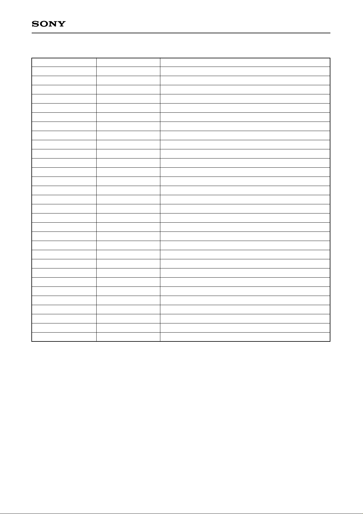
Pin Description
Pin No.
1
2
3
4
5
6
7
8
9
10
11
12
13
14
15
16
17
18
19
20
21
22
23
24
25
26
27
28
29
30
Symbol
CL
DA
CE/ADSW
BS3
BS1
BS2
BS4
VCC1
MIXOUT1
MIXOU2
GND1
BYP/MS
VHFIN
UHFIN1
UHFIN2
VOSC1
GND
VOSC2
UOSCB1
UOSCE1
UOSCE2
UOSCB2
VCC2
GND2
IFOUT
LOCK/ADC
VT
CPO
REFOSC
VCC3
Description
CLOCK/SCL (I2C bus)
DATA/SDA (I2C bus)
Enable/address selection (I2C bus)
Band switch output 3
Band switch output 1
Band switch output 2
Band switch output 4
Analog circuit VCC
MIX output
MIX output
Analog circuit GND
VHF input GND and control bus switching
VHF input
UHF input
UHF input
VHF oscillator (base input)
GND
VHF oscillator (collector output)
UHF oscillator (base pin)
UHF oscillator (emitter pin)
UHF oscillator (emitter pin)
UHF oscillator (base pin)
PLL circuit VCC
PLL circuit GND
IF output
LOCK signal output/ADC input (I2C bus)
VC drive voltage output (open collector)
Charge pump output (loop filter connection)
Crystal connection
Band switch power supply
Page 4
—4—
CXA3250AN
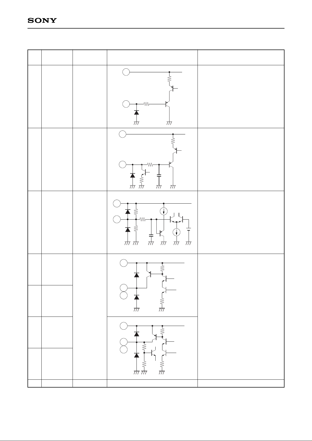
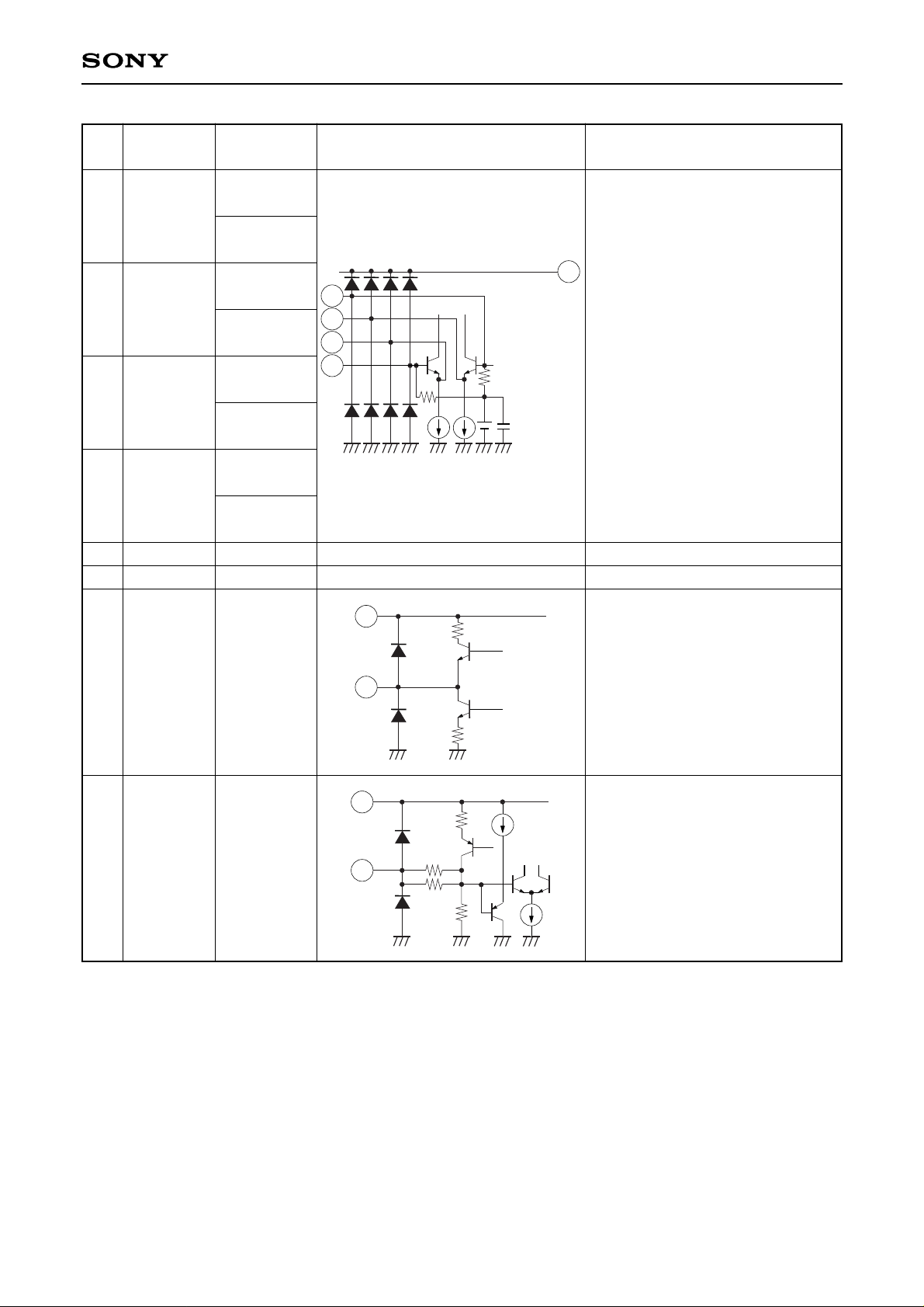
Pin Description and Equivalent Circuit
Pin
Symbol
Pin voltage
Equivalent circuit Description
No. [V]
1
2
3
4
7
5
6
8
CL
DA
ADSW/CE
BS3
BS4
BS1
BS2
VCC1
—
—
1.25
(when open)
ON : 4.8
OFF : 0.0
—
40k
1
23
40k
2.5p
2
23
20
150k
50k
5p
3
23
7
30
4
6
30
5
25k
12k
Clock input.
Data input.
I2C bus setting :
Address selection.
Bits 1 and 2 of the address byte
are controlled.
3-wire bus setting :
Enable input.
Band switch outputs.
The pin corresponding to the
selected band goes High.
Analog circuit power supply.—
Page 5
—5—
CXA3250AN
Pin
Symbol
Pin voltage
Equivalent circuit Description
No. [V]
9
10
11
12
13
14
15
16
18
17
MIXOUT1
MIXOUT2
GND1
BYP/MS
VHFin
UHFin1
UHFin2
VOSC1
VOSC2
GND
—
—
—
3.8 during
VHF reception
3.8 during
UHF reception
2.6 during
VHF reception
0.1 during
UHF reception
2.6 during
UHF reception
0.1 during
VHF reception
2.6 during
UHF reception
0.1 during
VHF reception
2.1 during
VHF reception
2.3 during
UHF reception
4.2 during
VHF reception
5.0 during
UHF reception
—
9
10
24k
15p
3k 3k
76k
8
12
13
23
3k 3k
8
14
15
3k 3k
50
400
8
16
18
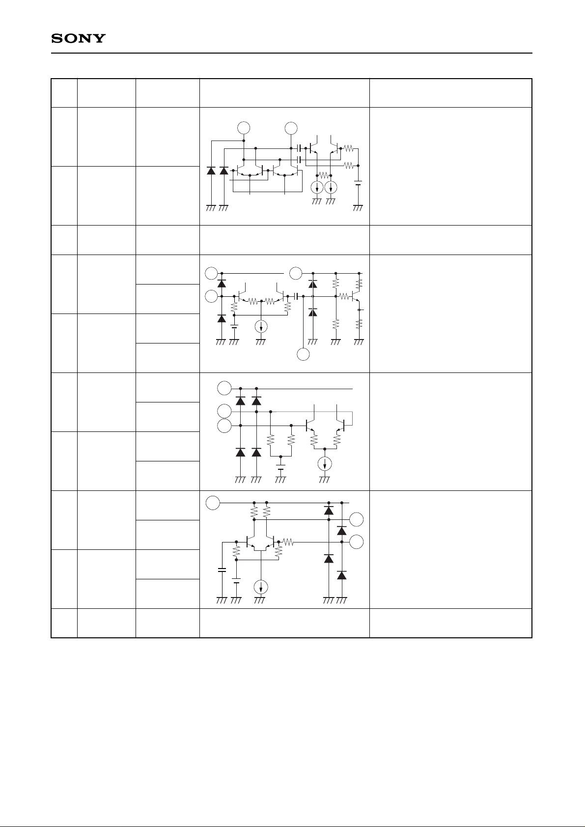
Mixer output.
These pins output the signal with
open collector, and they must be
connected to the power supply via
the load.
Analog circuit GND.
Pin 12 : VHF input grounding and
control bus switching.
Pin 13 : VHF input.
Input format is the
unbalanced input.
UHF inputs.
Input the signal to Pins 14 and 15
symmetrically or ground either of
Pin 14 or 15 with the capacitor and
input the signal to the rest.
External resonance circuit
connection for VHF oscillator.
GND for separating the analog and
PLL systems.
—
—
Page 6
—6—
CXA3250AN
Pin
Symbol
Pin voltage
Equivalent circuit Description
No. [V]
19
20
21
22
23
24
25
26
UOSCB1
UOSCE1
UOSCE2
UOSCB2
VCC2
GND2
IFOUT
LOCK/ADC
2.1 during
UHF reception
2.3 during
VHF reception
1.4 during
UHF reception
1.8 during
VHF reception
1.4 during
UHF reception
1.8 during
VHF reception
2.1 during
UHF reception
2.3 during
VHF reception
—
—
2.7
—
3k
3k
8
19
20
21
22
8
25
250
5k
500k
23
26
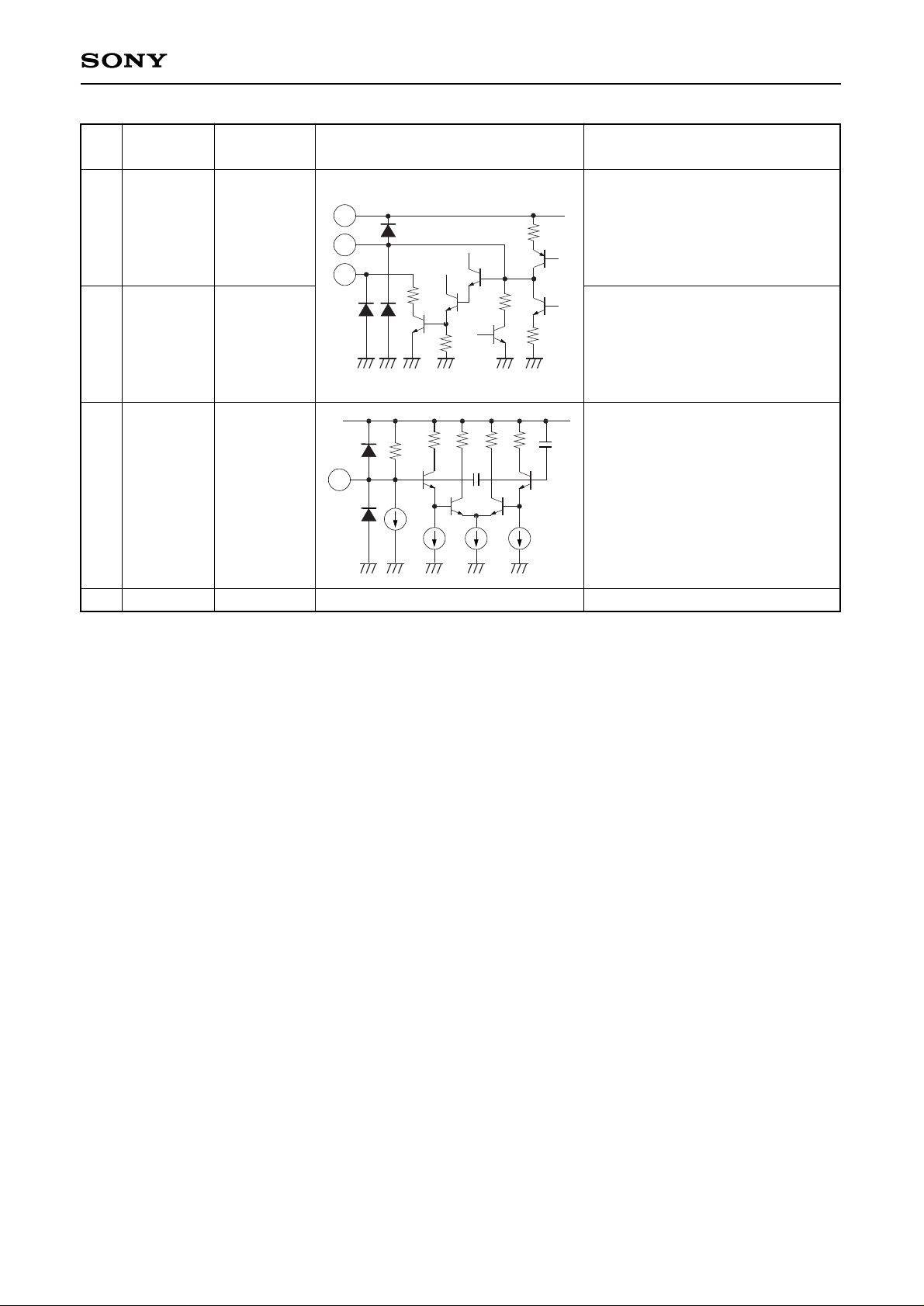
External resonance circuit
connection for UHF oscillator.
PLL circuit power supply.
PLL circuit GND.
IF output.
I2C bus setting :
5-level A/D converter input.
3-wire bus setting :
Lock detection.
Low when locked, High when
unlocked.
—
—
Page 7
—7—
CXA3250AN
Pin
Symbol
Pin voltage
Equivalent circuit Description
No. [V]
27
28
29
30
VT
CPO
REFOSC
VCC3
—
2.0
4.3
—
70
23
27
28
60k
30p
30p
29
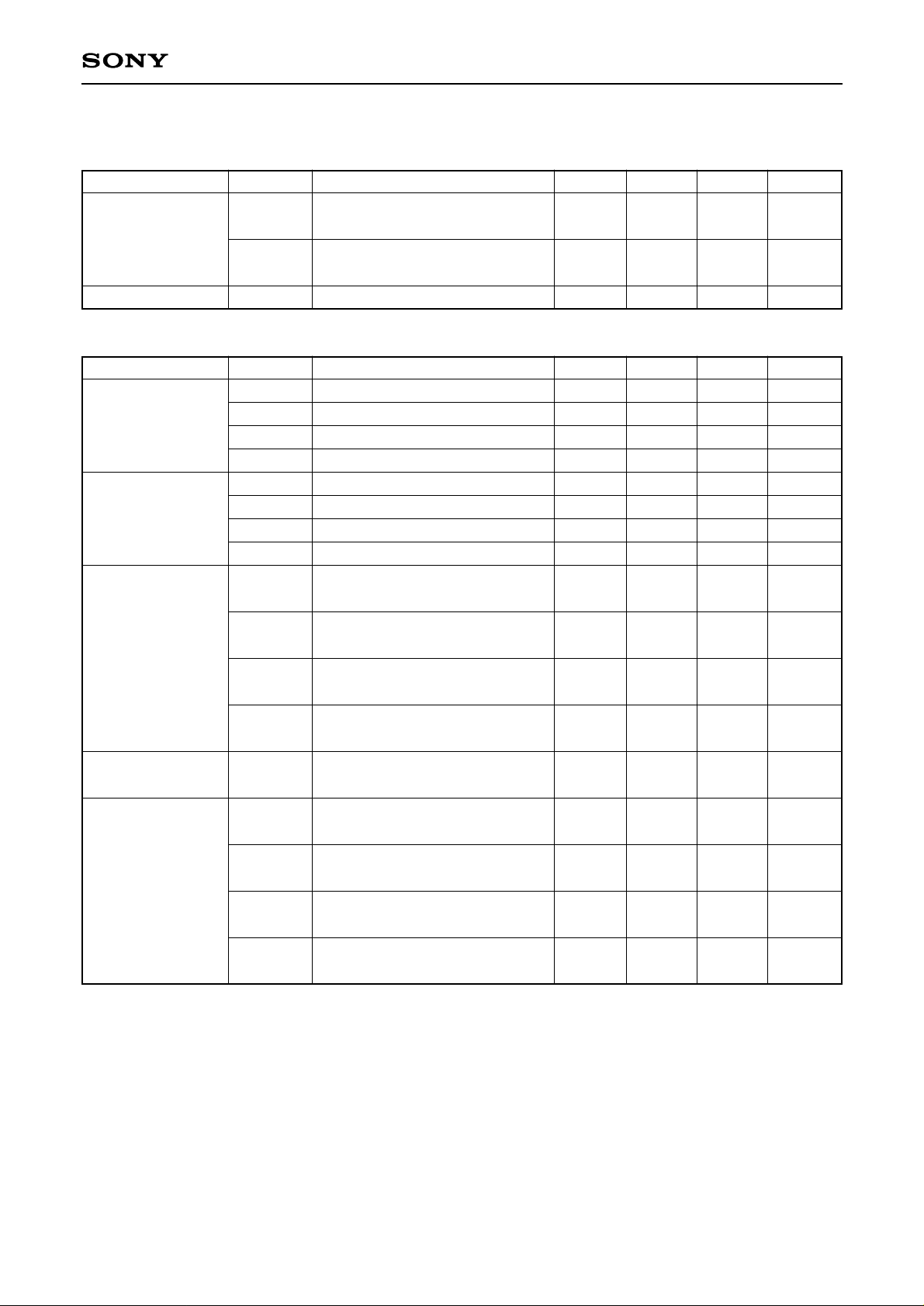
Varicap drive voltage output.
This pin outputs the signal with
open collector, and this must be
connected to the tuning power
supply via the load.
Charge pump output.
Connects the loop filter.
Crystal connection for reference
oscillator.
Power supply for external supply.—
Page 8
—8—
CXA3250AN
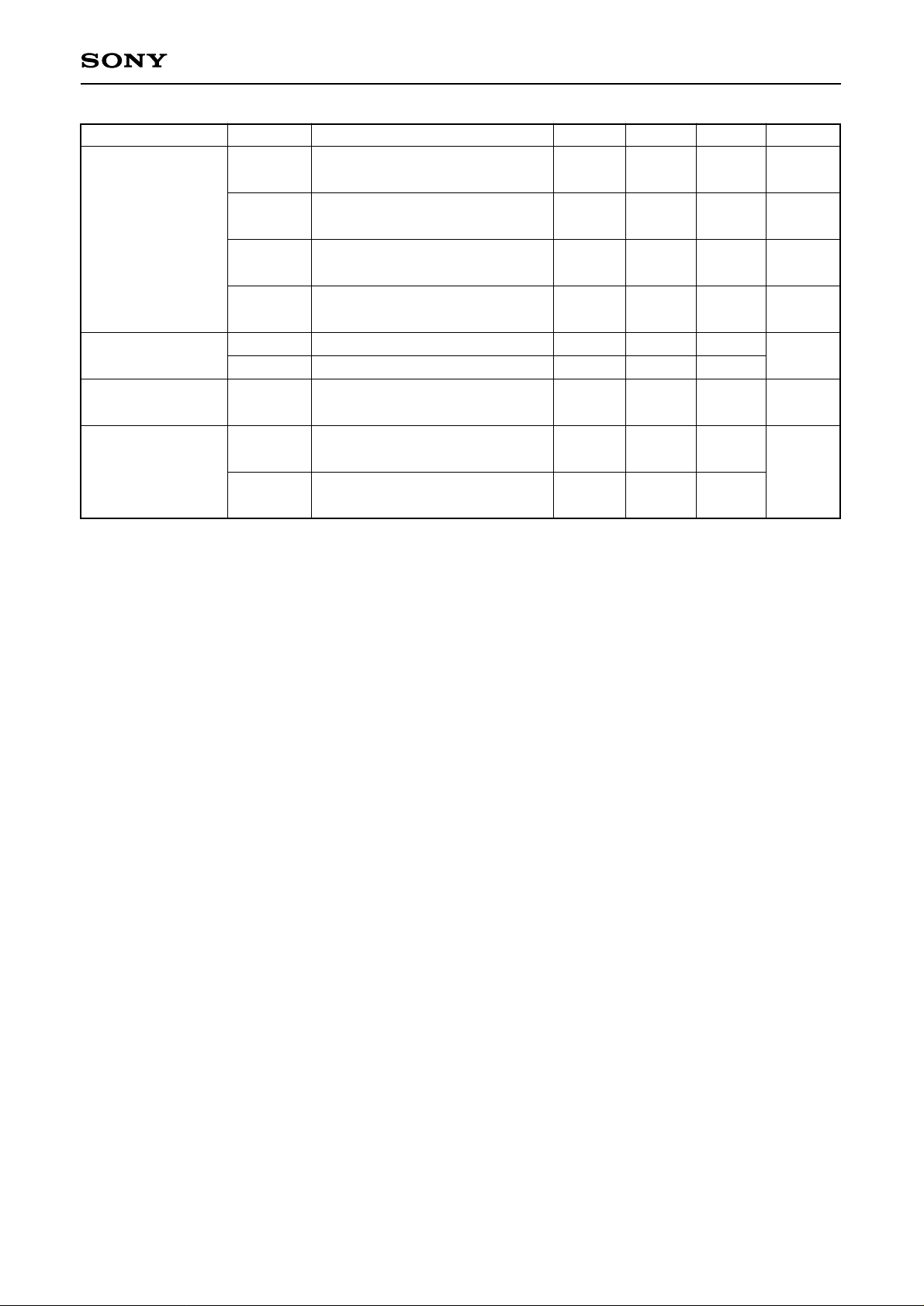
Electrical Characteristics
Circuit Current (VCC=5 V, Ta=25 °C)
Item
Circuit current A
Circuit current D
Symbol
AICCV
AICCU
DICC
Measurement conditions
VCC1 current, band switch output
open during VHF operation
VCC1 current, band switch output
open during UHF operation
VCC2 current
Min. Typ. Max. Unit
38 52 70 mA
39 53 71 mA
10 16 22 mA
Item
Conversion gain
Noise figure
∗1, ∗2
1 % cross
∗1, ∗3
modulation
Maximum output
power
Switch ON drift
∗4
Symbol
CG1
CG2
CG3
CG4
NF1
NF2
NF3
NF4
CM1
CM2
CM3
CM4
Pomax
∆ fsw1
∆ fsw2
∆ fsw3
∆ fsw4
Measurement conditions
VHF operation fRF=55 MHz
VHF operation fRF=360 MHz
UHF operation fRF=360 MHz
UHF operation fRF=800 MHz
VHF operation fRF=55 MHz
VHF operation fRF=360 MHz
UHF operation fRF=360 MHz
UHF operation fRF=800 MHz
VHF operation
fD=55 MHz, fUD=±12 MHz
VHF operation
fD=360 MHz, fUD=±12 MHz
UHF operation
fD=360 MHz, fUD=±12 MHz
UHF operation
fD=800 MHz, fUD=±12 MHz
50 Ω load saturation output
VHF operation fOSC=100 MHz
∆ f from 3 s to 3 min after switch ON
VHF operation fOSC=405 MHz
∆ f from 3 s to 3 min after switch ON
UHF operation fOSC=405 MHz
∆ f from 3 s to 3 min after switch ON
UHF operation fOSC=845 MHz
∆ f from 3 s to 3 min after switch ON
Min. Typ. Max. Unit
18 21 24 dB
19 22 25 dB
22.5 25.5 28.5 dB
24 27 30 dB
12 15 dB
11 14 dB
10 13 dB
11 14 dB
100 104 dBµ
99 103 dBµ
96 100 dBµ
90 94 dBµ
+8 +11 dBm
±300 kHz
±600 kHz
±350 kHz
±350 kHz
OSC/MIX/IF Amplifier Block
Page 9
—9—
CXA3250AN
Item
Supply voltage ∗4
drift
Oscillator phase
noise
Reference leak
Lock-up time
Symbol
∆ fst1
∆ fst2
∆ fst3
∆ fst4
C/N V
C/N U
REFL
LUT 1
LUT 2
Measurement conditions
VHF operation fOSC=100 MHz
∆ f when VCC 5 V changes ±5 %
VHF operation fOSC=405 MHz
∆f when VCC 5 V changes ±5 %
UHF operation fOSC=405 MHz
∆ f when VCC 5 V changes ±5 %
UHF operation fOSC=845 MHz
∆f when VCC 5 V changes ±5 %
10 kHz offset
10 kHz offset
Phase comparison frequency of
62.5 kHz, CP : 1
VHF operation fOSC=95 MHz ⇔
fOSC=395 MHz CP : 1
UHF operation fOSC=413 MHz ⇔
fOSC=847 MHz CP : 1
Min. Typ. Max. Unit
±200 kHz
±250 kHz
±150 kHz
±150 kHz
82
dBc/Hz
78
55 dB
24 70
ms
36 70
∗1 Value measured with untuned input.
∗2 NF meter direct-reading value (DSB measurement).
∗3 Value with a desired reception signal input level of –30 dBm, an interference signal of 100 kHz/30 % AM,
and an interference signal level where S/I=46 dB measured with a spectrum analyzer.
∗4 Value when the PLL is not operating.
Page 10
—10—
CXA3250AN
Item
CL, DA and CE pins
“H” level input voltage
“L” level input voltage
“H” level input current
“L” level input current
CE input
“H” level input voltage
“L” level input voltage
“H” level input current
“L” level input current
SDA output
“H” output leak current
“L” output voltage
CPO (charge pump)
Output current 1
Leak current 1
Output current 2
Leak current 2
VT (VC voltage output)
Maximum output voltage
Minimum output voltage
LOCK
“H” output voltage
“L” output voltage
REFOSC
Oscillation frequency range
Input capacitance
Negative resistance
Band SW
Output current
Saturation voltage
Leak current
Bus timing (I2C bus)
SCL clock frequency
Start waiting time
Start hold time
“L” hold time
“H” hold time
Start setup time
Data hold time
Data setup time
Symbol
VIH
VIL
IIH
IIL
VIH
VIL
IIH
IIL
ISDALK
VSDAL
ICPO1
LeakCP1
ICPO2
LeakCP2
VTH
VTL
VLOCKH
VLOCKL
FXTOSC
CXTOSC
RNEG
IBS
VSAT
LeakBS
fSCL
tWSTA
tHSTA
tLOW
tHIGH
tSSTA
tHDAT
tSDAT
Measurement conditions
VIH=VCC
VIL=GND
VIH=VCC
VIL=GND
Vin=5.5 V
Iout=–3 mA
Byte4/bit6=0
Byte4/bit6=0
Byte4/bit6=1
Byte4/bit6=1
When locked
When unlocked
Crystal source impedance
When ON
When ON Source current=20 mA
When OFF
Min. Typ. Max. Unit
3 VCC V
GND 1.5 V
0 –0.1 µA
–0.3 –4 µA
3 VCC V
GND 1.5 V
–100 –200 µA
35 100 µA
5 µA
GND 0.4 V
±35 ±50 ±75 µA
30 nA
±140 ±200 ±300 µA
100 nA
33 V
0.5 0.8 V
VCC–0.5 VCC V
0 0.5 V
3 12 MHz
22 24 26 pF
–2.0 –1.0 kΩ
–25 mA
120 240 mV
0.5 3 µA
0 400 kHz
1300 ns
600 ns
1300 ns
600 ns
600 ns
0 900 ns
600 ns
PLL Block
Page 11
—11—
CXA3250AN
Item
Rise time
Fall time
Stop setup time
Bus timing (3-wire bus)
Data setup time
Data hold time
Enable waiting time
Enable setup time
Enable hold time
Symbol
tR
tF
tSSTO
tSD
tHD
tWE
tSE
tHE
Measurement conditions Min. Typ. Max. Unit
300 ns
300 ns
600 ns
300 ns
600 ns
300 ns
300 ns
600 ns
PLL Block
Page 12
—12—
CXA3250AN
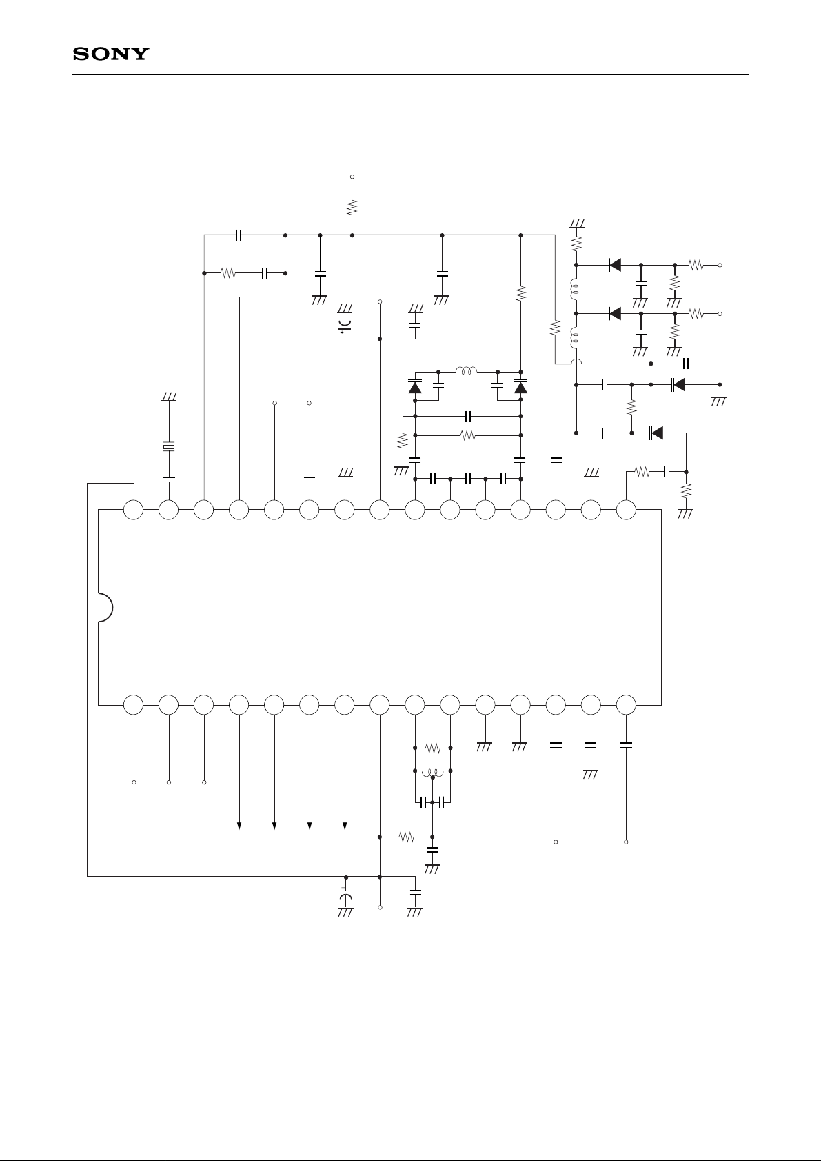
Electrical Characteristics Measurement Circuit (I2C bus control)
161718192021222324252627282930
CXA3250AN
CL
DA
CE/ADSW
BS3
BS1
BS2
BS4
V
CC1
MIX out1
MIX out2
GND1
BYP/MS
VHF in
UHF in1
UHF in2
V
CC3
REFOSC
CPO
VT
LOCK/ADC
IFOUT
GND2
V
CC2
UOSCB2
UOSCE2
UOSCE1
UOSCB1
VOSC2
GND
VOSC1
SCL SDA ADSW
FMT BVL BVH BU
+5V
2 3 4 8 9
10 11
12
13
14
15
1 5 6 7
1n
1n
2.2µ
2k
4.5t 4.5t
56p 56p
100
1n 1n 1n
VHF IN UHF IN
100p 1n
XTAL
4MHz
ADC in IF OUT
+5V
+30V
2.2µ 1n
2p
7p
6p 6p
56p 56p
1p
1T363 1T363
0.5p 0.5p
47k
47k
2.6φ
2.5t
3.2φ
2.5t
20 16p
47k
1n
150p
1T362
1T363
47k
47k
47k
47k
3.2φ
5.5t
6.8k 0.047µ
8200p
100p 33p
22k
0.75p
1n
51 BVH
47k
1n
51 BVL
1.2k
Page 13
—13—
CXA3250AN
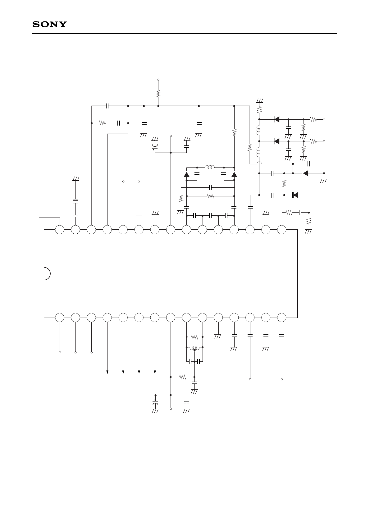
Electrical Characteristics Measurement Circuit (3-wire bus control)
161718192021222324252627282930
CXA3250AN
CL
DA
CE/ADSW
BS3
BS1
BS2
BS4
V
CC1
MIX out1
MIX out2
GND1
BYP/MS
VHF in
UHF in1
UHF in2
V
CC3
REFOSC
CPO
VT
LOCK/ADC
IFOUT
GND2
V
CC2
UOSCB2
UOSCE2
UOSCE1
UOSCB1
VOSC2
GND
VOSC1
SCL SDA CE
FMT BVL BVH BU
+5V
2 3 4 8 9
10 11
12
13
14
15
1 5 6 7
1n
1n
2.2µ
2k
4.5t 4.5t
56p 56p
100
1n1n 1n 1n
VHF IN UHF IN
100p 1n
XTAL
4MHz
LOCK IF OUT
+5V
+30V
2.2µ 1n
2p
7p
6p 6p
56p 56p
1p
1T363 1T363
0.5p 0.5p
47k
47k
2.6φ
2.5t
3.2φ
2.5t
20 16p
47k
1n
150p
1T362
1T363
47k
47k
47k
47k
3.2φ
5.5t
6.8k 0.047µ
8200p
100p 33p
22k
0.75p
1n
51 BVH
47k
1n
51 BVL
1.2k
Page 14

—14—
CXA3250AN
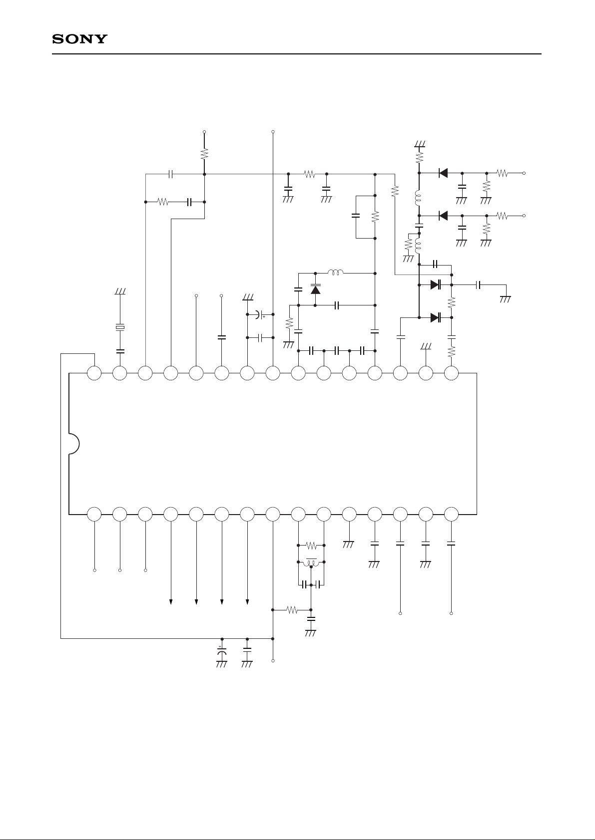
Application Circuit (I2C bus control)
CXA3250AN
CL
DA
CE/ADSW
BS4
BS3
BS2
BS1
V
CC1
MIX out1
MIX out2
GND1
BYP/MS
VHF in
UHF in1
UHF in2
V
CC3
REFOSC
CPO
VT
LOCK/ADC
IFOUT
GND2
V
CC2
UOSCB2
UOSCE2
UOSCE1
UOSCB1
VOSC2
GND
VOSC1
100p
XTAL
4MHz
5p
15p
16p 6p
100p 100p
2p
1T363
0.5p
10k
2.2φ
1.5t
3.2φ
2.5t
20
20p
0.5p
330p
150p
1T363
10k
2k
10k
10k
2p
10k
47k
3.2φ
5.5t
39k 82n
4.7n
1T362
1n
1.2k
47k
SWD
SWD
1n
1.2k
BVL
BVH
100
10k
1n 2.2n
+30V +5V
22k
1n
1n
ADC IN IF OUT
CL DA ADSW
FMT BVL BVH BU
+5V
1n
1n
3.3µ
4.5t 4.5t
56p 56p
100
1n 1n 1n
VHF IN UHF IN
161718192021222324252627282930
2 3 4 8 9
10 11
12
13
14
15
1 5 6 7
3.3µ
Application circuits shown are typical examples illustrating the operation of the devices. Sony cannot assume responsibility for
any problems arising out of the use of these circuits or for any infringement of third party patent and other right due to same.
Page 15
—15—
CXA3250AN
Application Circuit (3-wire bus control)
CXA3250AN
CL
DA
CE/ADSW
BS4
BS3
BS2
BS1
V
CC1
MIX out1
MIX out2
GND1
BYP/MS
VHF in
UHF in1
UHF in2
V
CC3
REFOSC
CPO
VT
LOCK/ADC
IFOUT
GND2
V
CC2
UOSCB2
UOSCE2
UOSCE1
UOSCB1
VOSC2
GND
VOSC1
100p
XTAL
4MHz
5p
15p
16p 6p
100p 100p
2p
1T363
0.5p
10k
2.2φ
1.5t
3.2φ
2.5t
20
20p
0.5p
330p
150p
1T363
10k
10k
10k
2p
10k
47k
3.2φ
5.5t
39k 82n
4.7n
1T362
1n
1.2k
47k
SWD
SWD
1n
1.2k
BVL
BVH
100
10k
1n 2.2n
10
+30V +5V
22k
1n
1n
LOCK IF OUT
CL DA CE
FMT BVL BVH BU
+5V
1n
1n
3.3µ
4.5t
2k
4.5t
56p 56p
100
1n1n 1n 1n
VHF IN UHF IN
161718192021222324252627282930
2 3 4 8 9
10 11
12
13
14
15
1 5 6 7
3.3µ
Application circuits shown are typical examples illustrating the operation of the devices. Sony cannot assume responsibility for
any problems arising out of the use of these circuits or for any infringement of third party patent and other right due to same.
Page 16

—16—
CXA3250AN
Description of Functions
The CXA3250AN is a ground wave broadcast tuner IC which converts frequencies to IF in order to tune and
detect only the desired reception frequency of VHF, CATV and UHF band signals.
In addition to the mixer, local oscillation and IF amplifier circuits required for frequency conversion to IF, this
IC also integrates a PLL circuit for local oscillation frequency control onto a single chip.
The functions of the various circuits are described below.
1. Mixer circuit
This circuit outputs the frequency difference between the signal input to VHFIN or UHFIN and the local
oscillation signal.
2. Local oscillation circuit
A VCO is formed by externally connecting an LC resonance circuit composed of a varicap diode and
inductance.
3. IF amplifier circuit
This circuit amplifies the mixer IF output, and consists of an amplifier stage and low impedance output
stage.
4. PLL circuit
This PLL circuit fixes the local oscillation frequency to the desired frequency. It consists of a programmable
divider, reference divider, phase comparator, charge pump and reference oscillator. The control format
supports both the I2C bus and 3-wire bus formats.
During I2C bus control, the frequency steps of 31.25, 50 or 62.5 kHz can be selected by the data-based
reference divider frequency division setting value.
During 3-wire bus control, these frequency steps can be selected by the combination of the communication
word length (18 or 19 bits) and the voltage applied to the BYP/MS pin.
5. Band switch circuit
The CXA3250AN has four sets of built-in PNP transistors for switching between the VL, VH and UHF bands
and for switching the FM trap, etc. These PNP transistors can be controlled by the bus data.
The emitters for these PNP transistors are connected to an independent power supply pin (VCC3) from the
oscillator, mixer and PLL circuits, and support either 5 V or 9 V as the RF amplifier power supply.
Page 17
—17—
CXA3250AN
Description of Analog Block Operation
(See the Electrical Characteristics Measurement Circuit.)
VHF oscillator circuit
• This circuit is a differential amplifier type oscillator circuit. Pin 18 is the output and Pin 16 is the input.
Oscillation is performed by connecting an LC resonance circuit including a varicap to Pin 18 via coupled
capacitance, inputting to Pin 16 with feedback capacitance, and applying positive feedback.
• The amplifier between Pins 16 and 18 has an extremely high gain. Therefore, care should be taken to
avoid creating parasitic capacitance, resistance or other feedback loops as this may produce abnormal
oscillation.
VHF mixer circuit
• The mixer circuit employs a double balanced mixer with little local oscillation signal leakage.
The input format is base input type, with Pin 12 grounded via a capacitor and the RF signal input to Pin
13. (Pin 12 can also be used to switch the PLL mode according to the applied DC voltage value.)
• The RF signal is fed from the oscillator, converted to IF frequency and output from Pins 9 and 10.
UHF oscillator circuit
• This oscillator circuit is designed so that two collector ground type Colpitts oscillators perform differential
oscillation operation via an LC resonance circuit including a varicap.
• Resonance capacitance is connected between Pins 19 and 20, Pins 20 and 21, and Pins 21 and 22, and
an LC resonance circuit including a varicap is connected between Pins 19 and 22.
UHF mixer circuit
• This circuit employs a double balanced mixer like the VHF mixer circuit.
The input format is base input type, with Pins 14 and 15 as the RF input pins. The input method can be
selected from balanced input consisting of differential input to Pins 14 and 15 or unbalanced input
consisting of grounding Pin 14 via a capacitor and input to Pin 15.
• Pins 9 and 10 are the mixer outputs.
IF amplifier circuit
• The signals frequency converted by the mixer are output from Pins 9 and 10, and at the same time are
AC coupled inside the IC and input to the IF amplifier.
• Single-tuned filters are connected to Pins 9 and 10 in order to improve the interference characteristics of
the IF amplifier.
• The signal amplified by the IF amplifier is output from Pin 25.
The output impedance is approximately 75 Ω.
Page 18
—18—
CXA3250AN
Description of PLL Block
This IC supports both I2C bus and 3-wire bus control.
The I2C bus conforms to the standard I2C bus format, and bidirectional bus control is possible consisting of a
write mode in which various data are received and a read mode in which various data are sent.
The 3-wire bus is equipped with an 18- or 19-bit auto identify function, and the frequency step can be
switched according to the voltage applied to the BYP/MS pin.
The PLL of this IC does not have a fixed frequency division circuit and performs high-speed phase
comparison, providing low reference leak and quick lock-up time characteristics.
During power-on (VCC2), the power-on reset circuit operates to initialize the frequency data to all “0” and the
band data to all “OFF”. Power-on reset is performed when Vcc2=2.5 V at room temperature (Ta=25 °C).
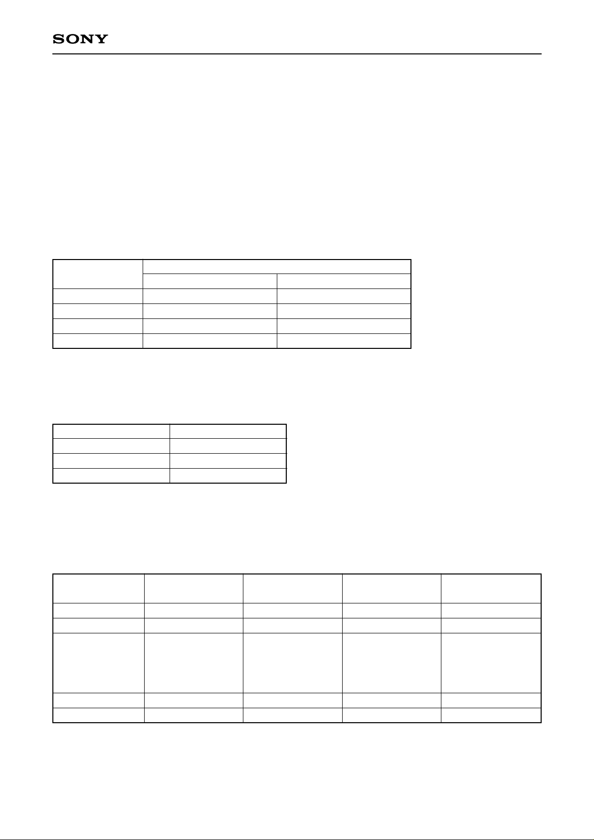
Pin Function Table
1.) PLL Mode Setting Method
The selected control bus is set according to the BYP/MS pin (Pin 12) voltage.
During 3-wire bus control, the transferred bit length (18, 19 or 27 bits) is automatically identified.
During 18- or 19-bit transfer, the frequency steps in the table below are set according to the combination of
the BYP/MS pin voltage and the bit length. This IC does not have a fixed frequency division circuit, so the
phase comparison frequency becomes the frequency step.
Symbol
CL
DA
ADSW/CE
LOCK/ADC
I2C bus
SCL input
SDA I/O
Address selection
ADC input
3-wire bus
CLOCK input
DATA input
ENABLE input
LOCK output
BYP/MS pin
GND
OPEN
VCC
Control bus
I2C bus
3-wire bus
3-wire bus
BYP/MS
pin voltage
OPEN
OPEN
OPEN
or
VCC
VCC
VCC
Transfer bit length
18
19
27
18
19
Reference
divider
64
128
Selectable from
64, 80 or 128
80
80
Phase comparison
frequency
62.5 kHz
31.25 kHz
62.5 kHz/
50.0 kHz/
31.25 kHz
50.0 kHz
50.0 kHz
Frequency
step∗
62.5 kHz
31.25 kHz
62.5 kHz/
50.0 kHz/
31.25 kHz
50.0 kHz
50.0 kHz
∗ Phase comparison frequency and frequency step are for when the crystal oscillation=4 MHz.
Page 19

—19—
CXA3250AN
2.) Programming
The VCO lock frequency is obtained according to the following formula.
fosc=fref × (32 M + S)
fosc: local oscillator frequency
fref : phase comparison frequency
M : main divider frequency division ratio
S : swallow counter frequency division ratio
The variable frequency division ranges of M and S are as follows, and are set as binary.
S < M ≤ 1023 (S < M ≤ 511 during 18-bit transfer)
0 ≤ S ≤ 31
3.) I2C Bus Control
This IC conforms to the standard I2C bus format, and bidirectional bus control is possible consisting of a
write mode in which various data are received and a read mode in which various data are sent. Write and
read modes are recognized according to the setting of the final bit (R/W bit) of the address byte. Write
mode is set when the R/W bit is “0” and read mode is set when the R/W bit is “1”.
Page 20
—20—
CXA3250AN
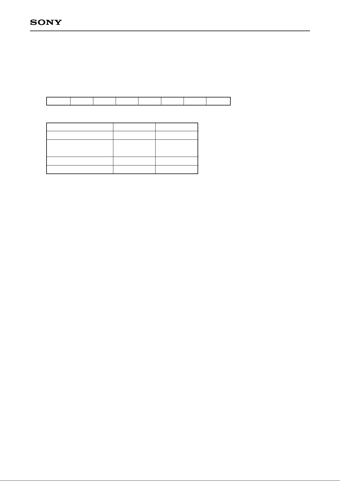
3-1) Address settings
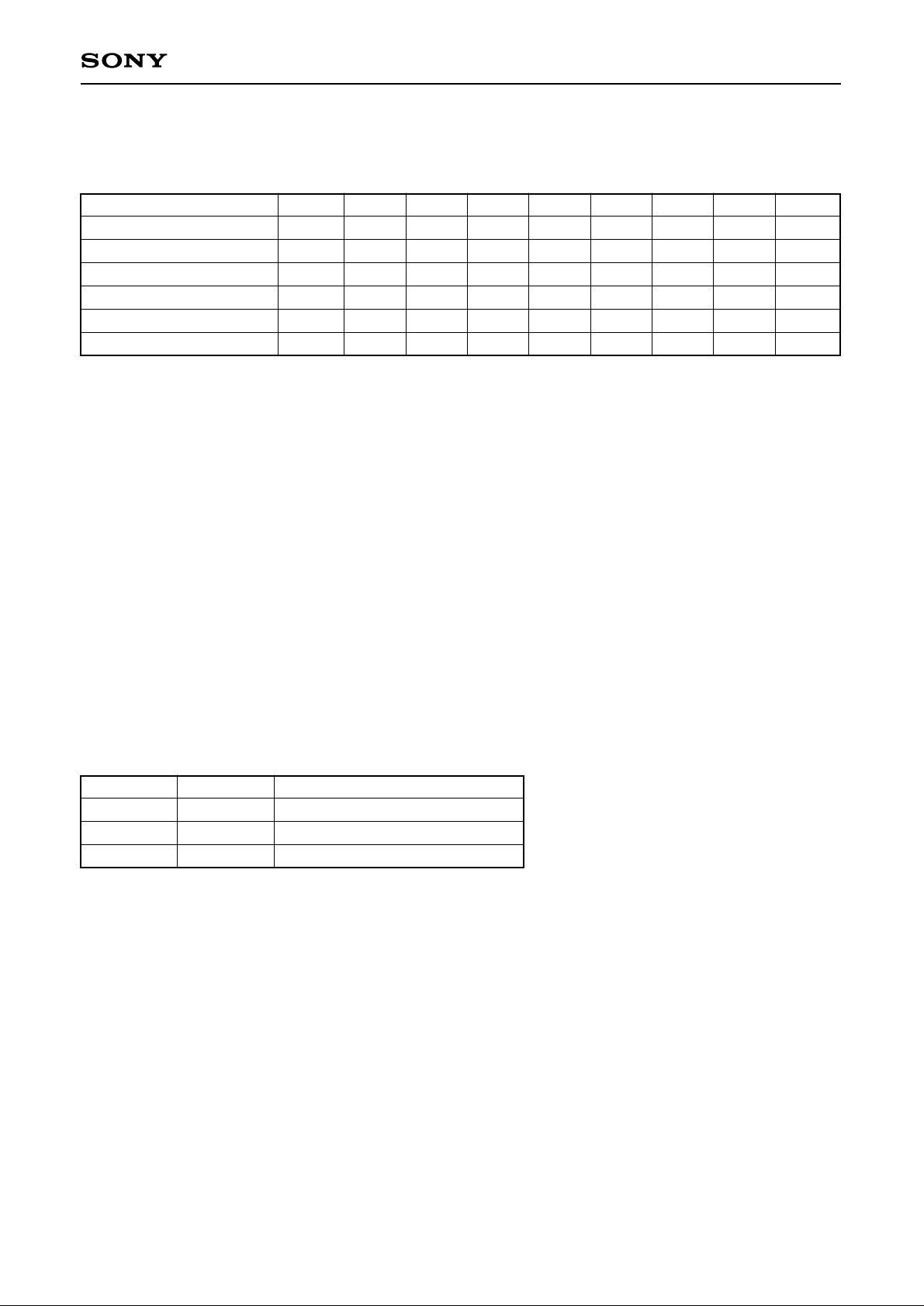
Up to four addresses can be selected by the hardware bit settings, so that multiple PLL can exist within
one system.
The responding address can be set according to the ADSW/CE pin voltage.
Address
Hardware bits
3-2) Write mode
Write mode is used to receive various data. In this mode, byte 1 contains the address data, bytes 2 and
3 contain the frequency data, byte 4 contains the control data, and byte 5 contains the band switch data.
These data are latch transferred in the manner of byte 1, byte 2 + byte 3, and byte 4 + byte 5.
When the correct address is received and acknowledged, the data is recognized as frequency data if the
first bit of the next byte is “0”, and as control data and band switch data if this bit is “1”.
Also, when data transmission is stopped part-way, the previously programmed data is valid. Therefore,
once the control and band switch data have been programmed, 3-byte commands consisting of the
address and frequency data are possible.
Further, even if the I2C bus stop conditions are not met, data can be input by sending the start
conditions and the new address.
1 1 0 0 0 MA1 MA0 R/W
CE pin voltage
0 to 0.1 VCC
OPEN or
0.2 VCC to 0.3 VCC
0.4 VCC to 0.6 VCC
0.9 VCC to VCC
MA1
0
0
1
1
MA0
0
1
0
1
Page 21
—21—
CXA3250AN
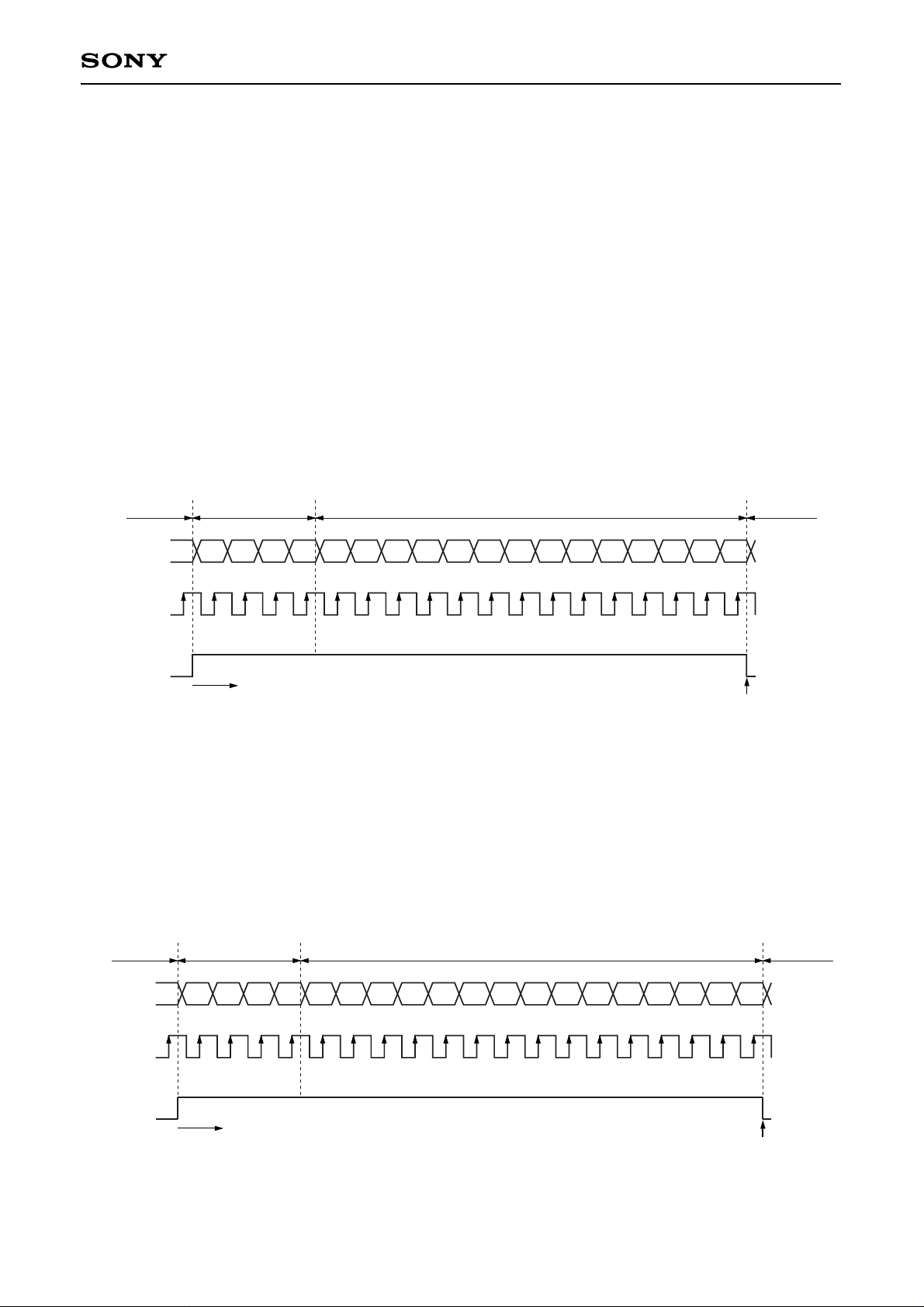
The control format is as shown in the table below.
Write-mode : Slave Receiver
MODE
Address byte
Divider byte 1
Divider byte 2
Control byte
Band SW byte
MSB LSB
bit7 bit6 bit5 bit4 bit3 bit2 bit1 bit0
1 1 0 0 0 MA1 MA0 0 A
0 M9 M8 M7 M6 M5 M4 M3 A
M2 M1 M0 S4 S3 S2 S1 S0 A
1 CP 0 CD X R1 R0 OS A
X X X X BS4 BS3 BS2 BS1 A
X : Don’t care
A : Acknowledge bit
MA0, MA1 : address setting
M0 to : main divider frequency division ratio setting
S0 to : swallow counter frequency division ratio setting
CD : charge pump OFF (when “1”)
OS : varicap output OFF (when “1”)
CP : charge pump current switching (200 µA when “1”, 50 µA when “0”)
BS1 to BS4 : band switch control (output PNP transistor ON when “1”)
R0, R1 : reference divider frequency division ratio setting.
See the Reference Divider Frequency Division Ratio Table.
Reference Divider Frequency Division Ratio Table
Reference divider
128
64
80
R1
0
1
X
R0
1
1
0
X : Don’t care
Page 22

—22—
CXA3250AN
3-3) Read mode
In read mode, the phase comparator locked/unlocked status and 5-level A/D converter input pin voltage
status are transmitted and output to the master.
The read data format is as shown in the table below.
Read mode : Slave Transmitter
A : Acknowledge bit
MA0, MA1 : address setting
FL : lock detection signal (1: locked, 0: unlocked)
A0 to A1 : A/D converter (See the table below.)
5-level A/D Converter Output Table
MODE
Address byte
Status byte
bit7 bit6 bit5 bit4 bit3 bit2 bit1 bit0
1 1 0 0 0 MA1 MA0 0 A
X FL 1 1 1 A2 A1 A0 A
Voltage applied to LOCK/ADC pin
0.6 VCC2 to VCC2
0.45 VCC2 to 0.6 VCC2
0.3 VCC2 to 0.45 VCC2
0.15 VCC2 to 0.3 VCC2
0 to 0.15 VCC2
A1
1
0
0
0
0
A1
0
1
1
0
0
A0
0
1
0
1
0
Page 23
—23—
CXA3250AN
4.) 3-Wire Bus Control
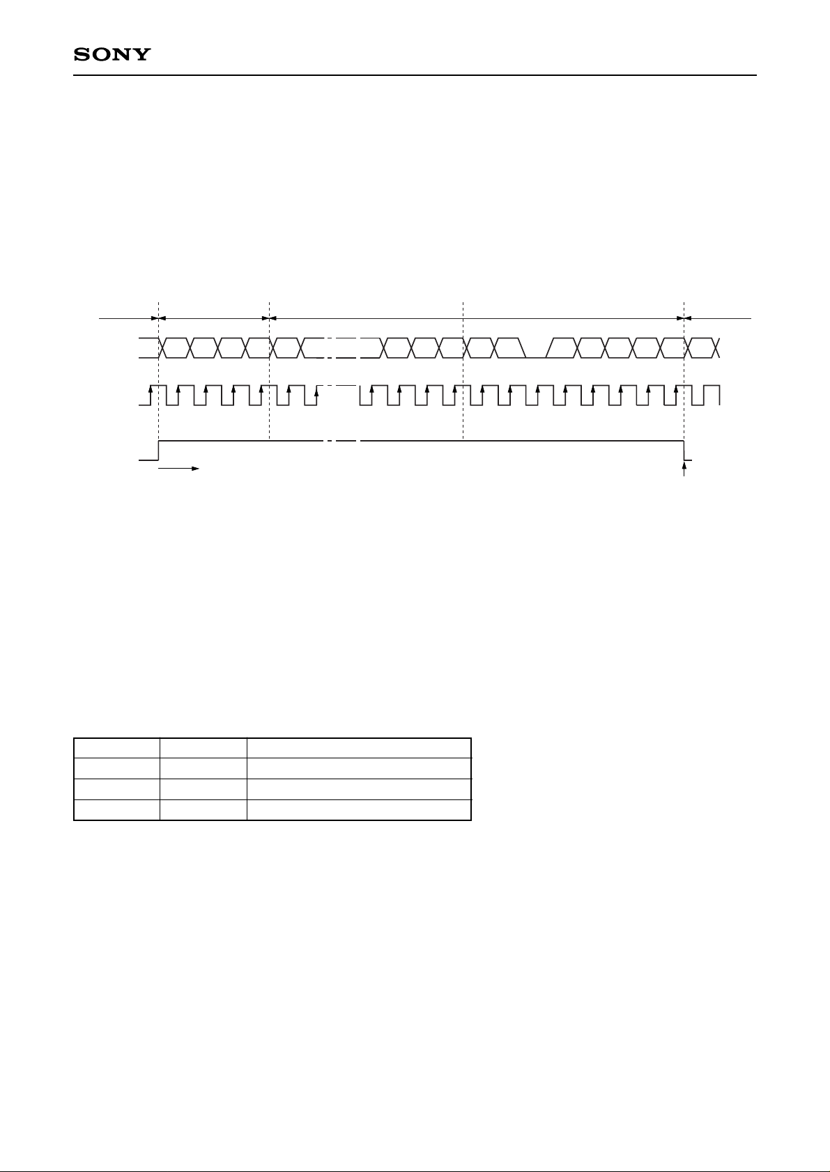
The following transfer bit length formats are automatically identified during 3-wire bus control.
18 bits : Band data (4 bits) + frequency data (14 bits)
19 bits : Band data (4 bits) + frequency data (15 bits)
27 bits : Band data (4 bits) + frequency data (15 bits) + test data (8 bits)
4-1) 18-bit data transfer
Data is loaded at the rising edge of the clock signal while the enable signal is high, and is latched at the
falling edge of the enable signal.
The clocks during the enable period are counted, and when 18 bits have been loaded, the
programmable divider “M9” data is set to “0” and the reference divider frequency division ratio is
automatically set to “1/80” when the BYP/MS pin voltage is VCC or to “1/64” when the BYP/MS pin is DC
open.
4-2) 19-bit data transfer
Data is loaded at the rising edge of the clock signal while the enable signal is high, and is latched at the
falling edge of the enable signal.
The clocks during the enable period are counted, and when 19 bits have been loaded, the reference
divider frequency division ratio is automatically set to “1/80” when the BYP/MS pin voltage is VCC or to
“1/128” when the BYP/MS pin is DC open.
1 4 5 18
BS4 BS3 BS2 BS1 M8 M7 M6 M5 M4 M3 M2 M1 M0 S4 S3 S2 S1 S0
DATA
CLOCK
ENABLE
Time Latch
Invalid data Invalid dataBand switch data Frequency data
18-bit data format
1 4 5 19
BS4 BS3 BS2 BS1 M8M9 M7 M6 M5 M4 M3 M2 M1 M0 S4 S3 S2 S1 S0
DATA
CLOCK
ENABLE
Time Latch
Invalid data Invalid dataBand switch data Frequency data
19-bit data format
Page 24
—24—
CXA3250AN
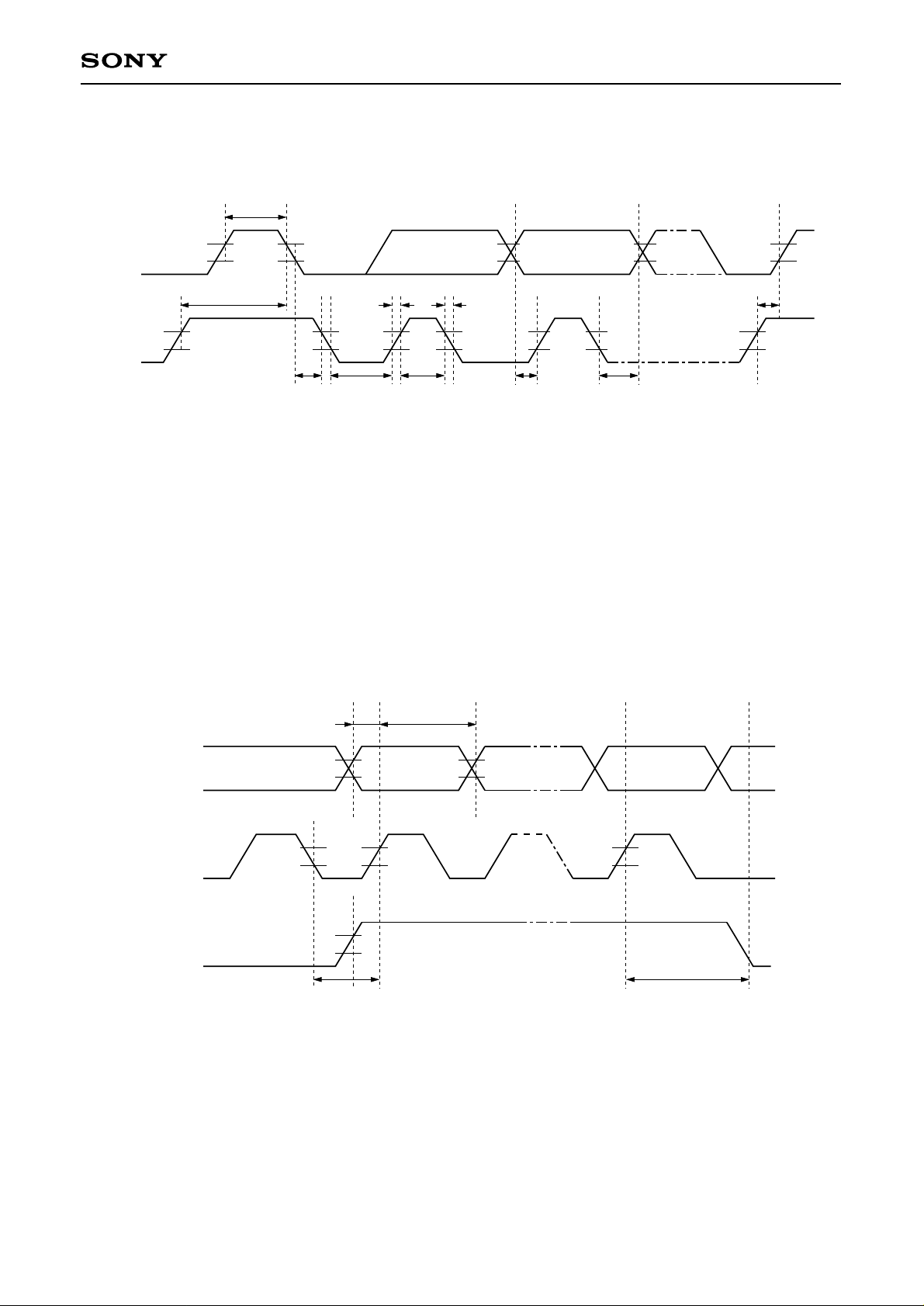
4-3) 27-bit data transfer
The 3-wire bus also automatically supports the 27-bit format in which various control data are
transferred in addition to the band and frequency data.
Data is loaded at the rising edge of the clock signal while the enable signal is high, and is latched at the
falling edge of the enable signal.
The clocks during the enable period are counted, and 27 bits of data as counted from the rising edge of
the enable signal are loaded as valid data.
M0 to : main divider frequency division ratio setting
S0 to : swallow counter frequency division ratio setting
CD : charge pump OFF (when “1”)
OS : varicap output OFF (when “1”)
CP : charge pump current switching (200 µA when “1”, 50 µA when “0”)
BS1 to BS4 : band switch control (output PNP transistor ON when “1”)
R0, R1 : Reference divider frequency division ratio setting.
Reference Divider Frequency Division Ratio Table
1 4 5 2719 20
BS4 BS3 BS2 BS1 M8M9 S3 S2 S1 S0 X CP CD X R1 R0 X
DATA
CLOCK
ENABLE
Time Latch
Invalid data Invalid dataBand switch data Frequency data Test data
27-bit data format
Reference divider
128
64
80
R1
0
1
X
R0
1
1
0
X : Don’t care
Page 25
—25—
CXA3250AN
I2C Bus Timing Chart
3-Wire Bus Timing Chart
tWSTA
tSSTA
tHSTA tLOW tHIGH tSDAT tHDAT
tR tF tSSTO
START STOPCLOCK DATACHANGE
t
SSTA=Start setup time
t
WSTA=Start waiting time
t
HSTA=Start hold time
t
LOW=LOW clock pulse width
t
HIGH=HIGH clock pulse width
tSDAT=Data setup time
t
HDAT=Data hold time
t
SSTO=Stop setup time
t
R =Rise time
t
F =Fall time
SDA
SCL
tHDtSD
tSD=Data setup time
t
HD=Data hold time
t
SE=Enable setup time
t
HE=Enable hold time
t
WE=Enable waiting time
DATA
CLOCK
ENABLE
3V
1.5V
3V
1.5V
3V
1.5V
tWE tHEtSE
Page 26
—26—
CXA3250AN
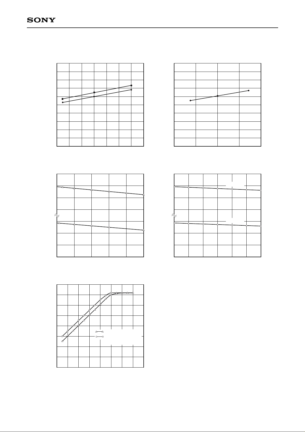
Example of Representative Characteristics
Circuit current vs. Supply voltage 1
AICC-Circuit current [mA]
VCC1-Supply voltage [V]
60
58
56
54
52
50
48
46
44
42
40
4.7 4.8 4.9 5 5.1 5.2 5.3 5.4
UHF
VHF
I/O characteristics (Untuned input)
IF output level [dBm]
RF level [dBm]
20
0
10
–20
–10
–40
–30
–60
–50
–60 –50 –40 –30 –20 –10 0
10 20
Circuit current vs. Supply voltage 2
DICC-Circuit current [mA]
VCC2-Supply voltage [V]
20
15
10
4.6 4.8 5 5.2 5.4
Band SW output voltage vs. Output current (BS1, BS2, BS3, BS4)
Output voltage [V]
Output current [mA]
9.2
9.0
8.8
8.6
5.0
4.8
4.6
4.4
0 5 10 15 20 25
V
CC3=9V
V
CC3=5V
Band SW output voltage vs. Output current
Output voltage [V]
Output current [mA]
9.2
9.0
8.8
8.6
5.0
4.8
4.6
4.4
0 1 2 3 4 5 6
fRF=145MHz (VHF)
f
RF=495MHz (UHF)
f
IF is both f=45MHz
VCC3=9V
V
CC3=5V
Page 27

—27—
CXA3250AN
Conversion gain vs. Reception frequency (Untuned input)
CG-Conversion gain [dB]
Reception frequency [MHz]
40
30
20
10
0
0 100 300200 400 500 600 700 800 900
UHF
fIF=45MHz
Next adjacent cross modulation vs. Reception frequency
(Untuned input)
CM-Cross modulation [dBµ]
Reception frequency [MHz]
Noise figure vs. Reception frequency (Untuned input, in DSB)
NF-Noise figure [dB]
Reception frequency [MHz]
VHF (High)
PCS beat characteristics
IF output level [dBm]
SG output level [dBm] (fP level)
+20
0
+10
–10
–20
–30
–40
–50
–60
–70
–80
+B drift [kHz]
20
15
10
5
0
0 100 300200 400 500 600 700 800 900
UHF
VHF (Low)
VHF (High)
fIF=45MHz
120
80
100
60
40
20
0
0 100 300200 400 500 600 700 800 900
fIF=45MHz
f
UD=fD+12MHz
f
UD=fD–12MHz
(100kHz, 30%AM)
UHF
Oscillation frequency power supply fluctuation (PLL off)
400
Oscillation frequency [MHz]
100
200
300
0
–100
–200
–300
–400
0 100 300200 400 500 600 700 800 900
VCC–5%
V
CC+5%
(V
CC=5V)
VHF (Low)
VHF (High)
–30–40 –10–20 0 +10 +20
fBeat
fIF
fLocal=95MHz
f
P=49.25MHz
f
C=52.83MHz (fP–12dB)
f
S=53.75MHz (fP–1.7dB)
fIF=45.75MHz
f
Beat=fIF±920kHz
VHF (Low)
VHF (Low)
Page 28
—28—
CXA3250AN
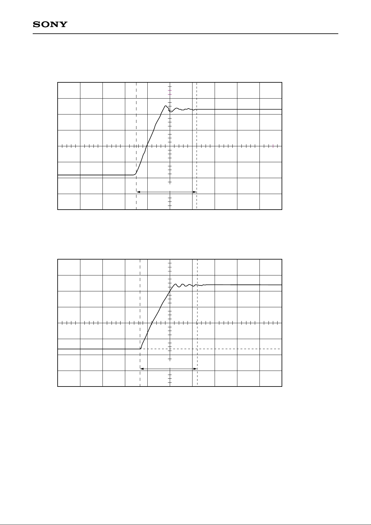
Tuning Response Time 1
VHF (Low) 95MHz → VHF (High) 395MHz (CP=1)
VHF (Low) 95MHz → VHF (High) 395MHz (CP=0)
–40,0000ms 10,0000ms
10.0ms/div
60,0000ms
real time
5.0V/div
offset 10.0V
T=27.2msec
–130,000ms 20,0000ms
30.0ms/div
170,000ms
real time
5.0V/div
offset 10.0V
T=75.6msec
Page 29

—29—
CXA3250AN
Tuning Response Time 2
UHF 413MHz → UHF 847MHz (CP=1)
UHF 413MHz → UHF 847MHz (CP=0)
–40,0000ms 10,0000ms
10.0ms/div
60,0000ms
real time
5.0V/div
offset 10.0V
T=34.2msec
–70,0000ms 30,0000ms
20.0ms/div
130,000ms
real time
5.0V/div
offset 10.0V 10.0V
T=86.0msec
Page 30
—30—
CXA3250AN
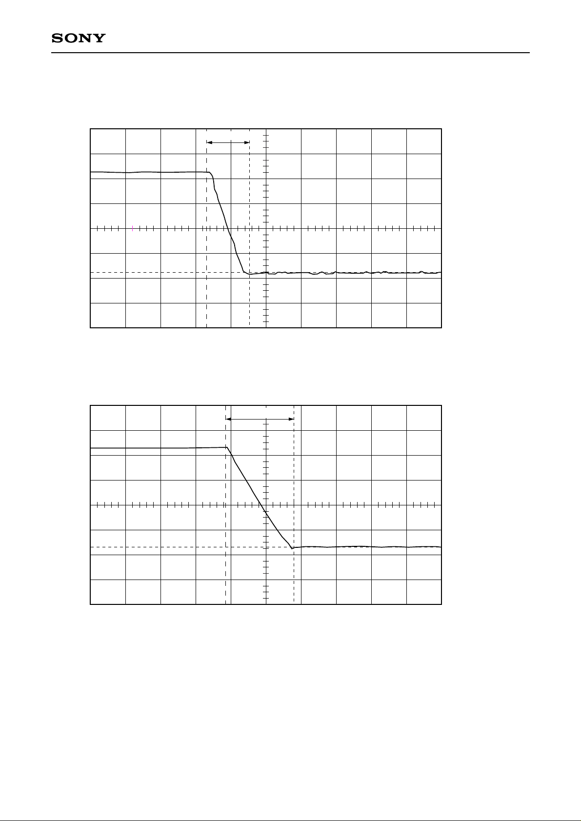
Tuning Response Time 3
VHF (High) 395MHz → VHF (Low) 95MHz (CP=1)
VHF (High) 395MHz → VHF (Low) 95MHz (CP=0)
–40,0000ms
10,0000ms
10.0ms/div
60,0000ms
real time
5.0V/div
offset 10.0V
T=12.6msec
–100,000ms 0,00000s
20.0ms/div
100,000ms
real time
5.0V/div
offset 10.0V
T=39.2msec
Page 31

—31—
CXA3250AN
Tuning Response Time 4
UHF 847MHz → UHF 413MHz (CP=1)
UHF 847MHz → UHF 413MHz (CP=0)
–40,0000ms 10,0000ms
20.0ms/div
600,000ms
real time
5.0V/div
offset 10.0V
T=15.0msec
–100,000ms 0,00000s
20.0ms/div
100,000ms
real time
5.0V/div
offset 10.0V
T=50.0msec
Page 32
—32—
CXA3250AN
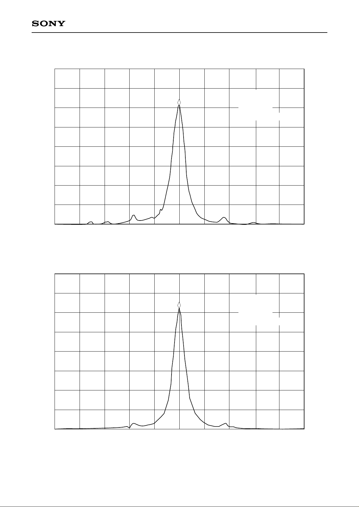
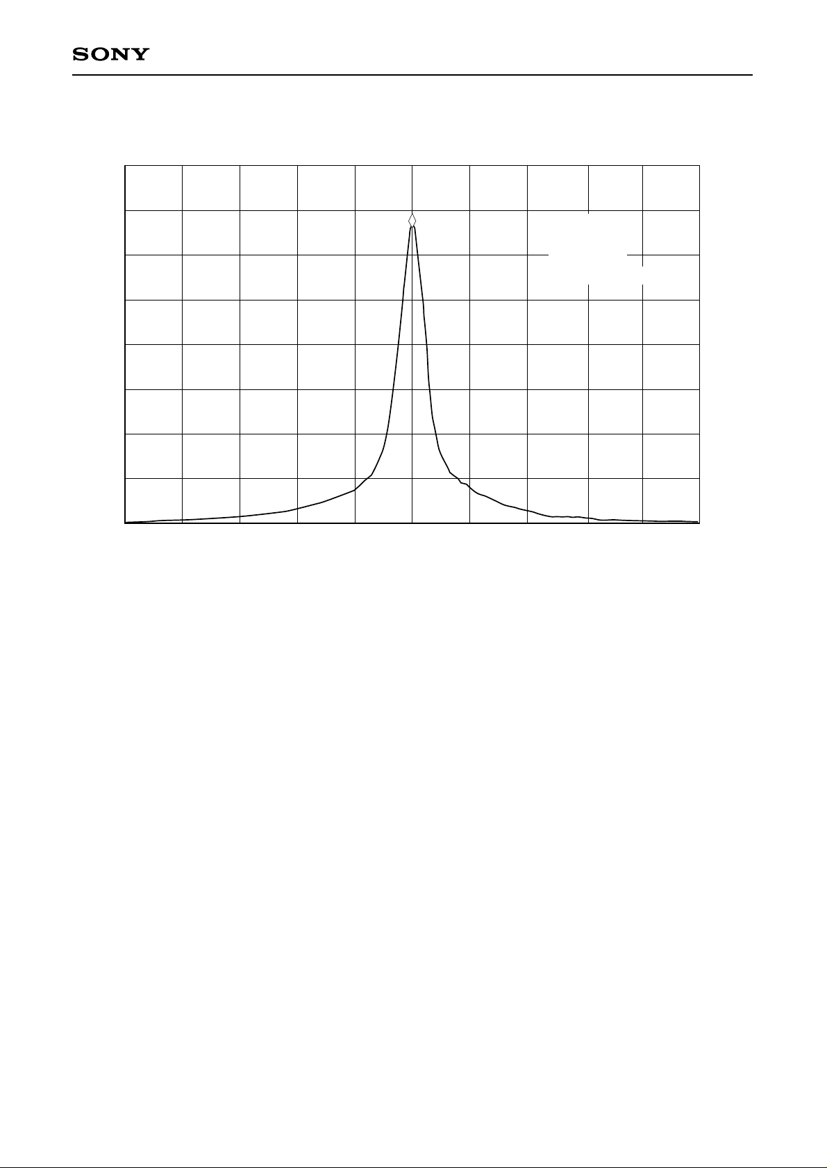
IF output spectrum
CENTER 45.0MHz
#RES BW 1.0kHz
SPAN 100.0kHz
SWP 30.0 sec#VBW 10Hz
10dB/div
VHF (Low)
fRF=55MHz
fL.0=100MHz
RF input level : –40dBm
IF output spectrum
CENTER 45.0MHz
#RES BW 1.0kHz
SPAN 100.0kHz
SWP 30.0 sec#VBW 10Hz
10dB/div
VHF (High)
fRF=350MHz
fL.0=395MHz
RF input level : –40dBm
Page 33
—33—
CXA3250AN
IF output spectrum
CENTER 45.0 270MHz
#RES BW 1.0kHz
SPAN 100.0kHz
SWP 30.0 sec#VBW 10Hz
10dB/div
UHF
fRF=800MHz
fL.0=845MHz
RF input level : –40dBm
Page 34
—34—
CXA3250AN
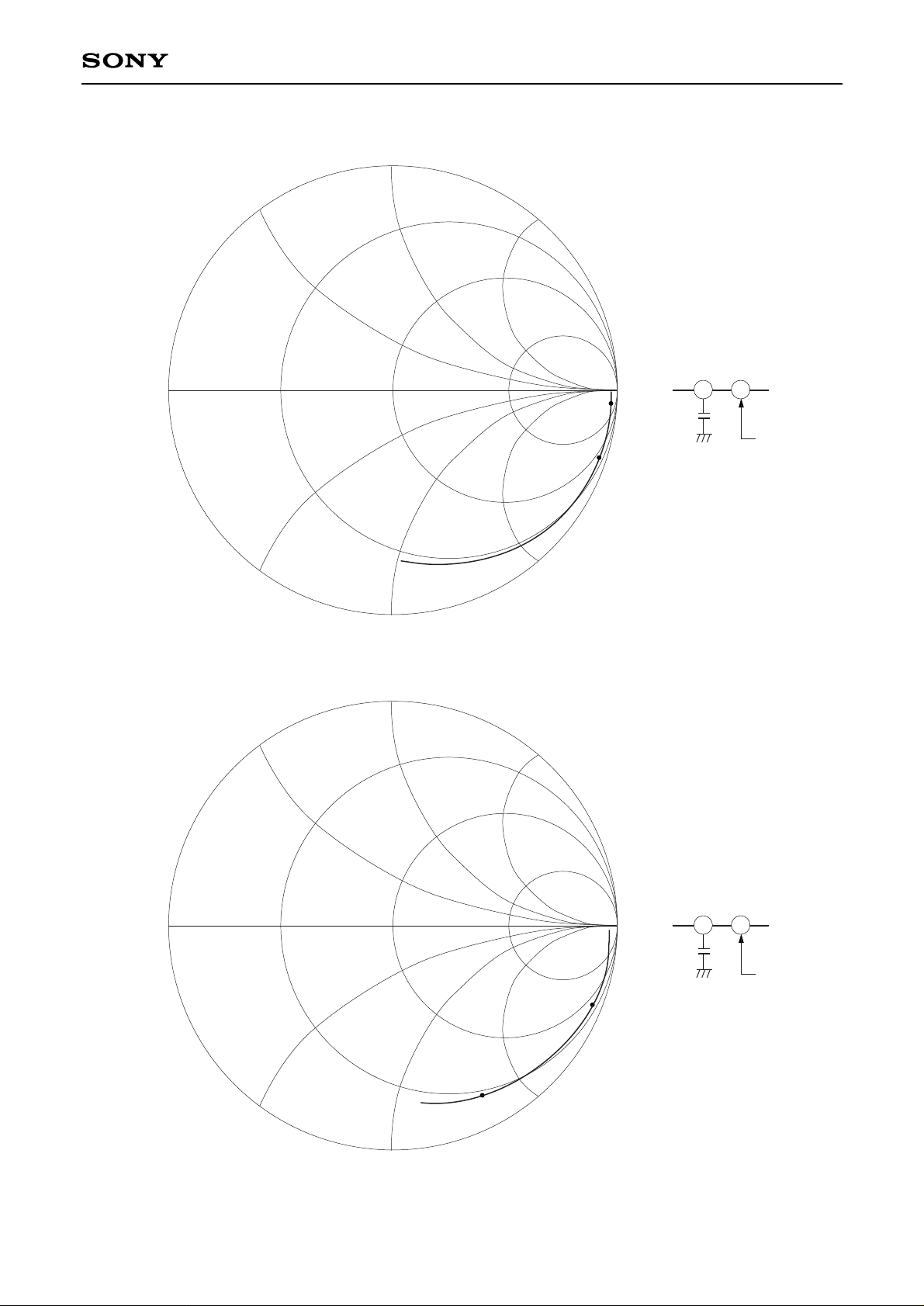
VHF Input Impedance
j100
j50
j25
0
–j25
–j50
–j100
50
1000p
S11
BYP/MS
VHFin
50MHz
350MHz
12 13
UHF Input Impedance
j100
j50
j25
0
–j25
–j50
–j100
50
S11
1000p
UHFin1
UHFin2
350MHz
800MHz
14
15
Page 35

—35—
CXA3250AN
IF Output Impedance
j100
j50
j25
0
–j25
–j50
–j100
50
45MHz
38MHz
Page 36
CXA3250AN
—36—
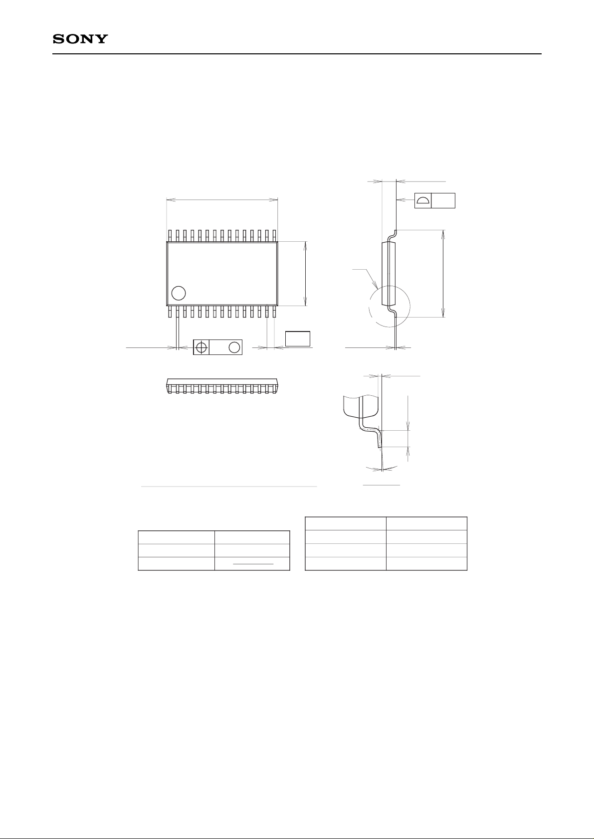
SONY CODE
EIAJ CODE
JEDEC CODE
PACKAGE STRUCTURE
PACKAGE MATERIAL
LEAD TREATMENT
LEAD MATERIAL
PACKAGE MASS
EPOXY RESIN
SOLDER/PALLADIUM
42/COPPER ALLOY
30PIN SSOP (PLASTIC)
∗9.7 ± 0.1
∗5.6 ± 0.1
0.65
0.22 – 0.05
30
1 15
16
1.25
+ 0.2
– 0.1
7.6 ± 0.2
0.15
+ 0.05
– 0.02
0.1 ± 0.1
0.5 ± 0.2
0° to 10°
A
DETAIL A
SSOP-30P-L01
SSOP030-P-0056
0.1g
NOTE: Dimension “∗” does not include mold protrusion.
PLATING
0.10
0.13
M
+ 0.1
Package Outline Unit : mm
NOTE : PALLADIUM PLATING
This product uses S-PdPPF (Sony Spec.-Palladium Pre-Plated Lead Frame).
 Loading...