

Page 1

Fingerprint Sensor
Description
The CXA3271GE is an electrostatic capacitance
method fingerprint sensor.
This monolithic IC integrates the sensor block, sense
amplifier (3-bit gain adjustment), sample-and-hold,
output amplifier and output buffer needed to acquire
fingerprint images, as well as the timing generator for
determining the operation of these functions onto a
single chip.
Features
• Electrostatic capacitance type sensor (charge transfer method)
• Number of pixels: 192 × 128
• 317 DPI
• Low power consumption (50mW or less)
• Single 3.3V power supply
• Sensor gain control: 3 bits
• S/N ratio improved by on-chip sensor block parasitic capacitance cancel function
Applications
Fingerprint verification units
Structure
Silicon gate CMOS IC
Absolute Maximum Ratings
• Supply voltage VDD VSS – 0.5 to +7.0 V
• Input voltage VI VSS – 0.5 to VDD + 0.5 V
• Output voltage VO VSS – 0.5 to VDD + 0.5 V
• Operating temperature Topr –20 to +75 °C
• Storage temperature Tstg –25 to +125 °C
• Allowable power dissipation PD 970 mW
Operating Conditions
• Supply voltage 3.15 to 3.45 V
• Recommended operating temperature 0 to +50 °C
– 1 –
E00235-PS
Sony reserves the right to change products and specifications without prior notice. This information does not convey any license by
any implication or otherwise under any patents or other right. Application circuits shown, if any, are typical examples illustrating the
operation of the devices. Sony cannot assume responsibility for any problems arising out of the use of these circuits.
CXA3271GE
30 pin LLGA
Page 2

– 2 –
CXA3271GE
Block Diagram
XSP (D/I)
CLK (D/I)
ADCLK (D/O)
UC UC
S_CNT
C_CLK
C_SP
Load
R_SP
R_CLK
UC UC UC UC
UC
UC
UC
UC
UC
UC UC
DI (D/I)
AOUT (A/O)
VOS (Bias)
3
3bit
DAC
Output
Buffer
192
128
Sense AMP (×192)
SENSOR
S/H & SW (×192)
Row Shift Register
Timing
Generator
Column Shift Register
........
128
.........
...........
192
...........
192
192
Page 3

– 3 –
CXA3271GE
Detailed Block Diagram
UC UC
C_CLK
UC UC UC
UC
UC
UC
UC
UC
UC
UC UC UC UC UCUC
192
55
D (1 to 192)
8
6
2
3
128
SENSOR (UC)
TG
XSP
MODEHDC_CLK
C_CK
R_LOG
DCLK
VCS_O
S (1 to 5)
S (1 to 5) N
C_SP
PG (1 to 128)
SRN (1 to 128)
........
128
.........
...........
192 (Dummy)
...........
.....................
192
..................
192
192
C_SP
C_COUT
C_LOG
SR
VOS
IN_N (1 to 192)
SC (1 to 192) SC (1 to 192) N
SC (1 to 192) SC (1 to 192) N
C_CO
CLK
XSP
SAMP (192)
S (1 to 5) N
S (1 to 5)VHVM
VL
DCLK
OUT
VCS_O
VH
VM
VL
OAMP
IN
DA AMP
OUT
VM
IN
DA AMP
OUT
VH
IN
DA AMP
OUT
VL
IN
DA AMP
OUT
VDS
DA
VS (1 to 8) N
BIAS_O
VS (3 to 8)
DEC
TEST1/2
DSELN
XSP
D1 (D to 2)
VS (3 to 8)
VS (1 to 8) N
BIAS_SA
AVDD (P/S)
AV
SS (P/S)
TEST1 (D/I)
TEST2 (D/I)
MODE (D/I)
DI0 (D/I)
DI1 (D/I)
DI2 (D/I)
XSP (D/I)
HD (D/I)
CLK (D/I)
C_CLK (D/I)
C_CK (D/O)
ADCLK (D/O)
RSRO (D/O)
CSRO (D/O)
DV
SS (P/S)
DV
SS (P/S)
DV
DD (P/S)
VCS_S (Bias)
VL (Bias)
VM (Bias)
VH (Bias)
VOS (Bias)
VCS_O (Bias)
AOUT (A/O)
AV
SS (P/S)
AV
DD (P/S)
Pin Symbol
2C
2D
2E
2F
3B
3C
3D
3E
3F
4B
4C
4D
4E
4F
5F
5E
5D
5C
5B
6F
6E
6D
6C
6B
7F
7E
7D
7C
LAND No.
8
7
6
5
4
3
2
15
14
13
12
11
10
9
1
BUF
16
23
22
21
26
25
24
28
27
20
19
18
17
Page 4

– 4 –
CXA3271GE
Pin Description
Serial
No.
Land No. Symbol I/O Description
Substrate electrode (chip rear surface electrode) 3.3V.
Analog power supply 3.3V.
Analog GND.
Test mode selection. Connect to GND.
Test mode selection. Connect to GND.
Connect to GND.
Gain setting input. (LSB)
Gain setting input.
Gain setting input. (MSB)
Sense start pulse input (negative pulse).
The column and row shift registers and the timing generator are cleared
by this signal.
Connect to GND.
Main clock. (1 to 2MHz)
Column shift register clock.
Connect to C_CK (4E).
Column shift register clock output.
Connect to C_CLK (4D).
Outputs the internally delayed input clock.
Digital power supply 3.3V.
Digital GND.
Digital GND.
Column shift register final output. (Connection is not required.)
Row shift register final output. (Connection is not required.)
Output amplifier reference voltage monitor. (1.65V)
Sensor charge voltage monitor. (1 LSB = 80mV)
Adjustable within the range of 1.92 to 2.48V by the three bits DI[0:2].
Sense amplifier reference voltage monitor. (1.85V)
Dummy cell charge voltage monitor for canceling parasitic capacitance.
VL = 2VM – VH
Sense amplifier current source bias monitor.
(Do not connect.)
Substrate electrode (chip rear surface electrode) 3.3V.
Analog power supply 3.3V.
Analog GND.
Sensor output.
Output amplifier and output buffer current source bias monitor.
(Do not connect.)
1
2
3
4
5
6
7
8
9
10
11
12
13
14
19
18
17
16
15
24
23
22
21
20
28
27
26
25
2B
2C
2D
2E
2F
3B
3C
3D
3E
3F
4B
4C
4D
4E
4F
5B
5C
5D
5E
5F
6B
6C
6D
6E
6F
7B
7C
7D
7E
7F
SUB
AVDD
AVSS
TEST1
TEST2
MODE
DI0
DI1
DI2
XSP
HD
CLK
C_CLK
C_CK
ADCLK
DVDD
DVSS
DVSS
CSRO
RSRO
VOS
VH
VM
VL
VCS_S
SUB
AVDD
AVSS
AOUT
VCS_O
Power
Power
Power
D/I
D/I
D/I
D/I
D/I
D/I
D/I
D/I
D/I
D/I
D/O
D/O
Power
Power
Power
D/O
D/O
A/O
A/O
A/O
A/O
A/O
Power
Power
Power
A/O
A/O
Page 5

– 5 –
CXA3271GE
Electrical Characteristics
1. DC Characteristics (Topr = 25°C, Vss = 0V)
Timing Definition
CLK
tpr
V
DD
0V
V
DD
0V
V
DD
0V
tpf
Output
2. AC Characteristics (Topr = 25°C, Vss = 3.3V)
Item
Analog supply voltage
Digital supply voltage
Input voltage (High)
Input voltage (Low)
Output voltage (High) CMOS
Output voltage (Low) CMOS
Input leak current
Output voltage
Output voltage
Output voltage
Output voltage
Output voltage
Output voltage
Current consumption
Symbol
AVDD
DVDD
VIH
VIL
VIH
VIL
IL
VH
VH
VL
VL
VM
VOS
IDD
Conditions
CMOS input cell
CMOS input cell
VDD = 3.3V, IOH = –800µA
VDD = 3.3V, IOL = 2.4mA
CMOS input pin
VDD = 3.3V (D0 D1 D2) = (L L L)
VDD = 3.3V (D0 D1 D2) = (H H H)
VDD = 3.3V (D0 D1 D2) = (L L L)
VDD = 3.3V (D0 D1 D2) = (H H H)
VDD = 3.3V (D0 D1 D2) = (∗ ∗ ∗)
VDD = 3.3V (D0 D1 D2) = (∗ ∗ ∗)
VDD = 3.3V
Min.
3.15
3.15
0.7VDD
Vss
2.8
0
–5
1.75
1.55
4
Typ.
3.3
3.3
1.92
2.48
1.76
1.2
1.84
1.65
10
Max.
3.45
3.45
VDD
0.3VDD
3.3
0.4
5
1.92
1.75
14
Unit
V
V
V
V
V
V
µA
V
V
V
V
V
V
mA
Item
Clock input period
Output rise delay time
Output fall delay time
Number of sensor defects
Output voltage Air Level
Output voltage Water Level
Applicable pins
CLK
C_CK, ADCLK, RSRO, CSRO
C_CK, ADCLK, RSRO, CSRO
AOUT
AOUT
Symbol
tpr
tpf
Conditions
CL = 30pF
CL = 30pF
∗1
∗2
Min.
400
600
200
Typ. Max.
160
200
5
1300
Unit
ns
ns
ns
Sensors
mV
mV
Page 6

– 6 –
CXA3271GE
∗1
Output voltage Air Level means the output level in the condition where nothing is placed against the sensor
surface (in other words, in air). This rating value is obtained by measuring 32 points within one line of the
sensor output and then taking the average.
The gain setting for this measurement is (011).
∗2
Output voltage Water Level specifies the degree to which the output level changes from the Air Level when
a drop of water is placed on the sensor surface. However, it is unrealistic to place a drop of water on each
sensor surface when sorting products, so 32 virtual capacitors (parasitic capacitance equal to the level
when a drop of water is placed on the surface) are built into the sensor chip, and the average of these
output values is calculated. The difference from the Air Level noted above becomes the Water Level.
The gain setting for this measurement is (011).
Page 7

– 7 –
CXA3271GE
Electrical Characteristics Measurement Circuit
27
25
23
21
19
17
15
13
11
9
7
5
3
1
28
26
24
22
20
18
16
14
12
10
8
6
4
2
Digital input pin
Digital output pin
Analog output pin
AV
DD
AOUT/O
VOS/O
VM/O
VCS_S/O
0.1µF
0.1µF
0.1µF
DV
SS
CSRO/O
ADCLK/O
C_CLK/I
HD/I
DI2/I
DI0/I
TEST2/I
AV
SS
AVSS
VCS_O/O
VH/O
VL/O
DV
DD
DVSS
RSRO/O
C_CK/O
CLK/I
XSP/I
DI1/I
MODE/I
TEST1/I
AV
DD
1.0µF
Vcc
3.3V
1.0µF
0.1µF
30pF or more is added to each pin.
S1
Page 8
– 8 –
CXA3271GE
Application Circuit
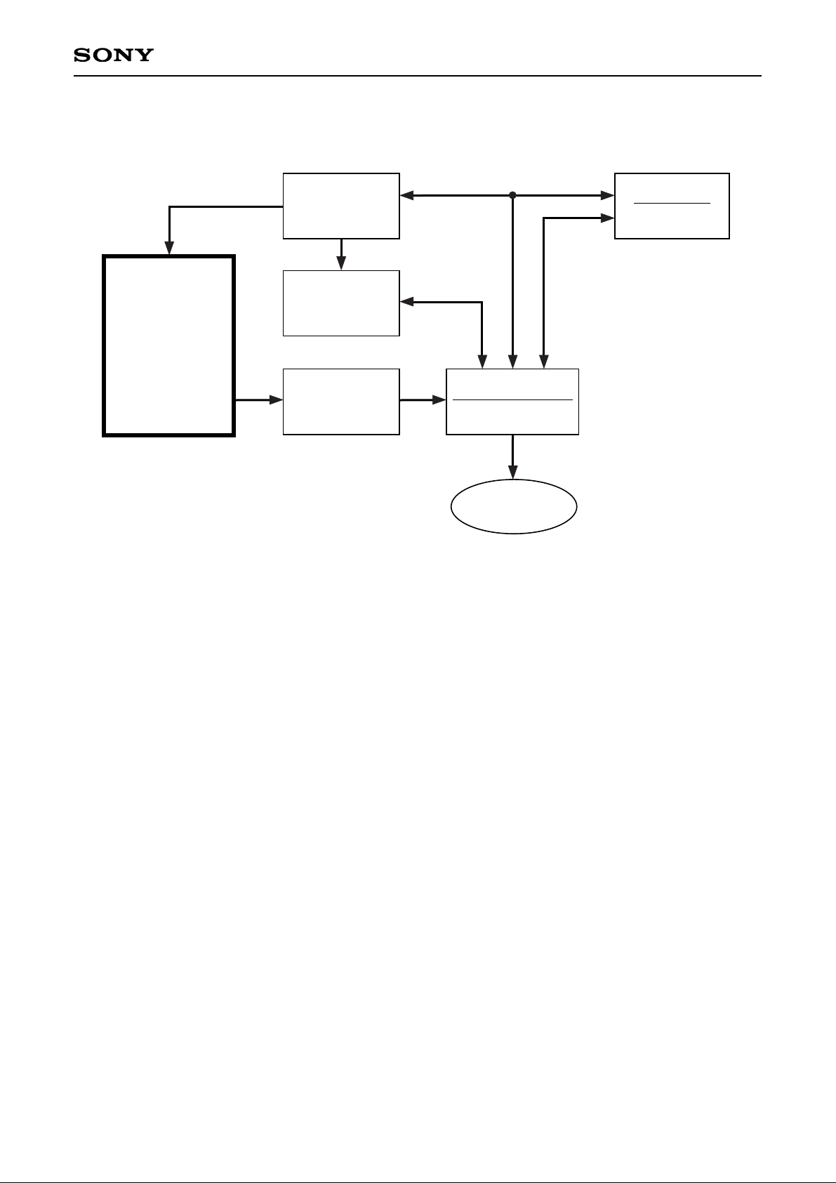
Microcomputer
DRAM
During
registration
During
verification
8-bit A/D
ASIC
Binary value, verification
Verification results
Fingerprint sensor chip
Flash
Registered data
Application circuits shown are typical examples illustrating the operation of the devices. Sony cannot assume responsibility for
any problems arising out of the use of these circuits or for any infringement of third party patent and other right due to same.
Page 9

– 9 –
CXA3271GE
,
,
Ridge Valley
Fingerprint unevenness
Over coat
Metal electrode
Inter-layer film
Si
Fig. 1
Description of Operation
• Fingerprint sensor principle
The principle of this newly developed fingerprint sensor
is described below. (Fig. 1) The sensor block contains an array of metal electrodes which are covered on top
by an insulating film (over coat). When a finger (which is conductive matter) is placed directly against this
surface, the three elements of the metal electrode, the insulating film and the finger form a capacitor.
The difference between the fingerprint ridges and valleys is the difference in distance to the metal electrodes,
and becomes the difference in the capacitance values of the individually formed capacitors. (The ridge
capacitance values are determined by the dielectric constant of the insulating film, but the valleys contain air
in addition to this, making the difference between the ridge and valley capacitance values even greater than
the difference in distance.)
Using this principle, by applying a constant voltage to all metal electrodes, the charge level accumulated in
each electrode differs, making it possible to output the unevenness of the fingerprint as an electric signal by
transferring and converting these charges to voltages.
Page 10

– 10 –
CXA3271GE
Sr
S4
S3
Cf1
Cf2
S6
S7
S11 S2 S1
VL
VM VH
Sense amplifier block
(192)
Output block
(1)
Sensor block
(192 × 128)
S5 Sc
Cs
Cp
Cp'
Vcel
Vsl
S_Amp
O_Amp
VOS
Ch2
Ch1
Voi Voo
Buf
Aout
Vdmy
Vsns
Fig. 2
• Fingerprint sensor operation (Fig. 2)
Description of characters
Cs: Capacitance formed between the finger and the metal electrode
Cp: Parasitic capacitance formed between the metal electrode and the silicon substrate
Cp': Capacitance for canceling Cp (Cp ≈ Cp')
Ch∗: Hold capacitance
Cf∗: Feedback capacitance for determining the gain
S∗: Switch
V∗: Node voltage
VH – VM ≈ VM – VL
• Detailed description of operation
(All switches are off in the default status.)
1. S1, S4, Sr and S11 are turned on, Vcel is set to voltage VH, and Vdmy is set to voltage VL.
Vcel accumulated charge (Cs + Cp) VH
Vdmy accumulated charge Cp' VL
2. S1, Sr and S11 are turned off.
3. S2 is turned on and Vsl is set to VM.
4. S4 is turned off.
5. Sr, S3 and S5 are turned on.
At this time, the charge level that moves from Vcel and Vdmy to Vsl (actually between capacitances) is:
(Cs + Cp) (VH – VM) – Cp' (VM – VL) ≈ Cs (VH – VM)
This means that the sense amplifier gain is determined independently of the parasitic capacitance,
making it possible to obtain the required large signal dynamic range.
Vsns = VM – Cs (VH – VM)/Cf1
The voltage Vsns determined as shown above is accumulated in Ch1.
6. S5 is turned off.
7. S6 is turned on and the Voi voltage is set to VOS.
8. S6 is turned off.
9. Sc and S7 are turned on.
At this time, the charge level that moves from Ch1 to Cf2 is:
(VOS – Vsns) Ch1
This determines the Voo voltage which is accumulated in Ch2 and output to Aout via the buffer.
Page 11
– 11 –
CXA3271GE
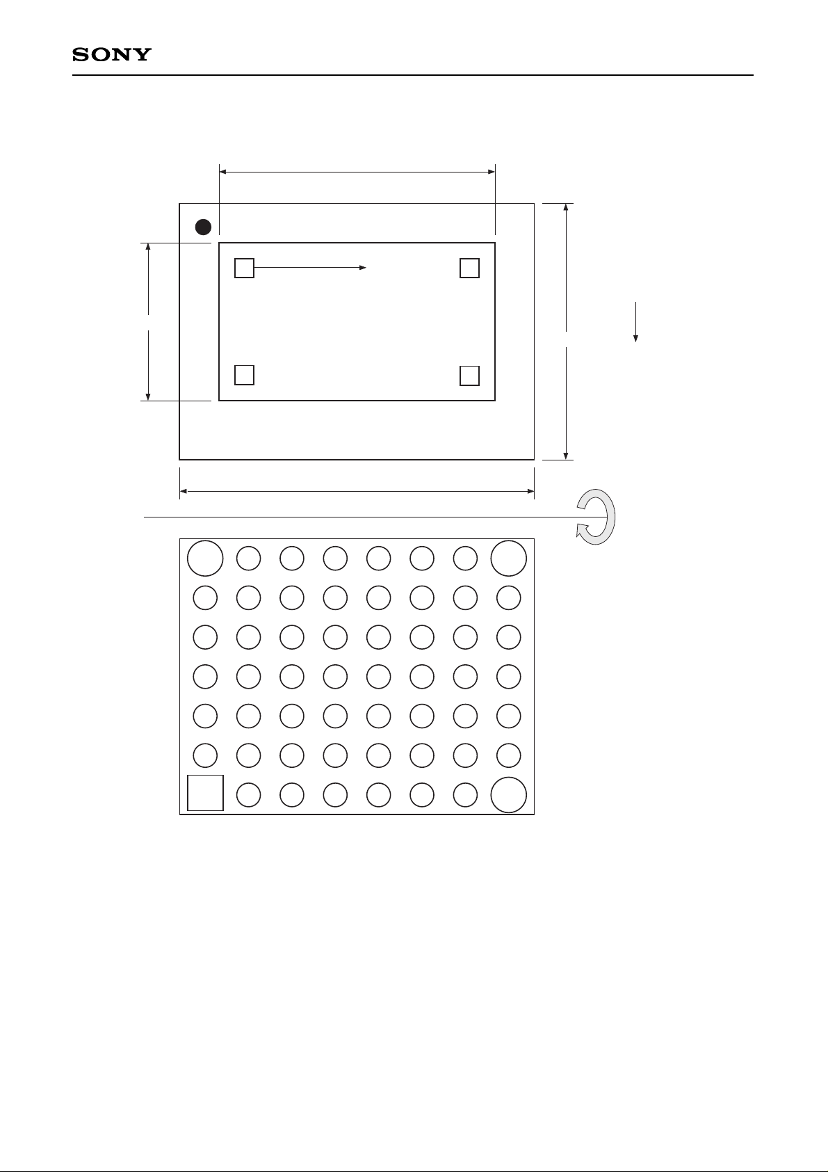
Appearance and Readout Order
15.36mm
19.8mm
Sensor Area
192 × 128
Scan Formation
Cell (1, 1) to Cell (1, 192)
Cell (128, 1) to
Cell (128, 192)
16.8mm
Flip
10.24mm
Cell (1, 1)
Cell (128, 1)
Cell (1, 192)
Cell (128, 192)
G
F
E
D
C
B
A
1 2 3 4 765 8
Page 12

– 12 –
CXA3271GE
Sr
S4
S3
Cf1
Cf2
S6
S7
S11 S2 S1
VL
VM VH
S5 Sc
Cs
Cp
Cp'
Vcel
Vsl
S_Amp
O_Amp
VOS
Ch2
Ch1
Voi Voo
Buf
Aout
Vdmy
Vsns
Notes on Operation
• Aout output variance
Aout output variance can be broadly classified into two types. The first is variance intrinsic to the IC, and the
second is variance caused by the influence of external noise due to the extremely high sensitivity.
• Variance intrinsic to the IC
1. The Aout output DC level fluctuates widely due to the IC.
This is caused by the Cp and Cp' capacitance values, the VM voltage level, the voltage differences VH – VM
and VM – VL, and the Vos voltage level in the figure above.
Vos, VH, VM and VL appear externally as pins. The Aout output level can be set to the desired potential
by applying the Vos voltage from an external source.
The Aout dynamic range is approximately 0.7 to 2.1V, so checking this output level and externally
applying the Vos voltage to set the optimum level is recommended.
2. 192 variances within one line
One line is comprised of 192 sensors. Each sensor is connected to a separate S_Amp, so the S_Amp
offset appears in the output. (approximately 100 to 200mV)
3. The DC level of a line changes with a certain regularity for some ICs. This is also caused by the S_Amp
DC offset.
• Variance due to the influence of external noise
1. Output fluctuation due to cross talk from the power supply
Power supply fluctuation has a large influence on the Aout output of this IC.
In addition to the capacitances between the power supply and GND (approximately 1µF, both sides if
possible), attaching capacitances of approximately 0.1µF to Vos, VH, VM and VL is recommended.
2. Finger stabilization
The human body acts as an antenna, so the finger potential changes during the sensing period, producing
noise in the Aout output. To prevent this, the potential of the area around the finger being sensed must be
equalized with the sensor GND. Measures such as placing a metal plate connected to GND around the
sensor so that the finger touches this place during sensing are recommended.
Page 13

– 13 –
CXA3271GE
Fingerprint sensors have the silicon chip directly exposed, so care should be taken for the following points. In
addition, a cover should be attached to protect the sensor surface during operation.
Sensor surface electrostatic strength
Contact discharge (150pF, 330Ω): ±1.25kV or more
Body charge (when the charge accumulated in the body is discharged over the sensor surface): ±4kV or more
Body charge differs between individuals.
Sensor surface strength
The sensor surface is covered with only a thin coating in order to acquire fingerprint information.
Therefore, care should be taken when handling the sensor.
Problems have been confirmed not to occur during the following tests.
• Pressing 10,000 times with a finger (Pressing time: 2s/time)
• Rubbing 10,000 times with a finger (Back and forth, 2s/time)
• Scratching with a fingernail (20 times back and forth)
• Rubbing strongly with a pencil (6H hardness) (20 times back and forth)
• Rubbing with a tissue (1,000 times back and forth)
Note that problems also occurred with the sensor surface during the following tests.
• Pressing strongly with a needle (normal sewing needle)
• Rubbing with an eraser
• Rubbing with the tip of a ball point pen
• Rubbing with steel wool
Page 14
– 14 –
CXA3271GE
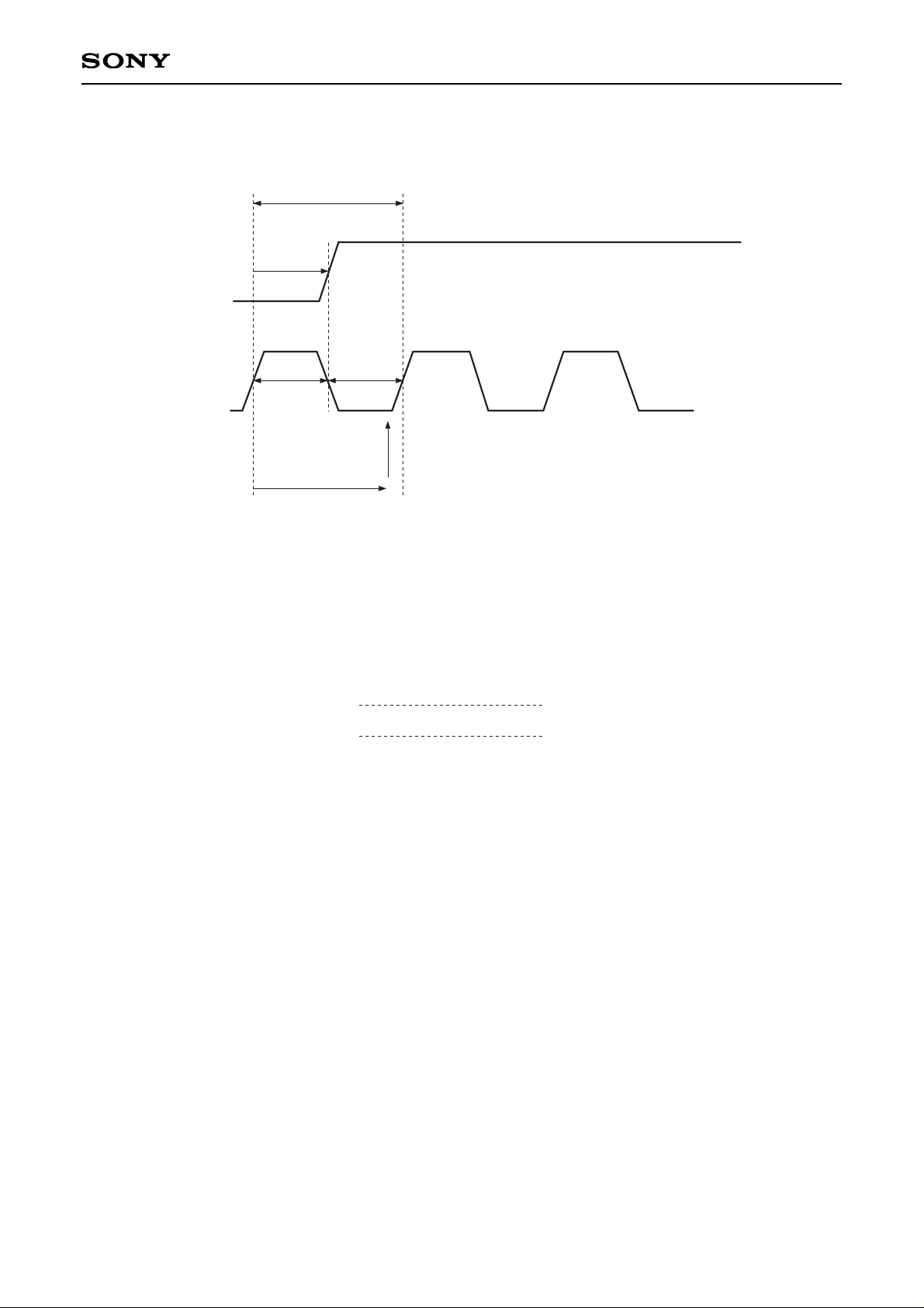
Timing Chart
500ns
XSP
(3F)
CLK
(4C)
Strobe
Point
Input level
V
IH = 0.7VDD
VIL = 0.3VDD
0.65VDD
0.35VDD
Output level
250ns
250ns
250ns
480ns
High
X
Low
Page 15

– 15 –
CXA3271GE
Input/output Signal
CLK
(4C)
Input
XSP
(3F)
Input
C_CK
(4E)
Output
RSRO
(5F)
Output
CSRO
(5E)
Output
Strobe point (CK Rise + 480ns)
500ns (1clk)
250ns
750ns
31.5µs
(63clk)
31.5µs
(63clk)
96.5µs
(193clk)
96.5µs
(193clk)
500ns
(1clk)
500ns
(1clk)
96µs
(192clk)
16384µs
(32768clk) {(193 + 63) × (2 + 126)}
128µs
(256clk)
500ns
(1clk)
256 clk
750ns
CK1 clock 2MHz
F = 2.0MHz
Page 16
– 16 –
CXA3271GE
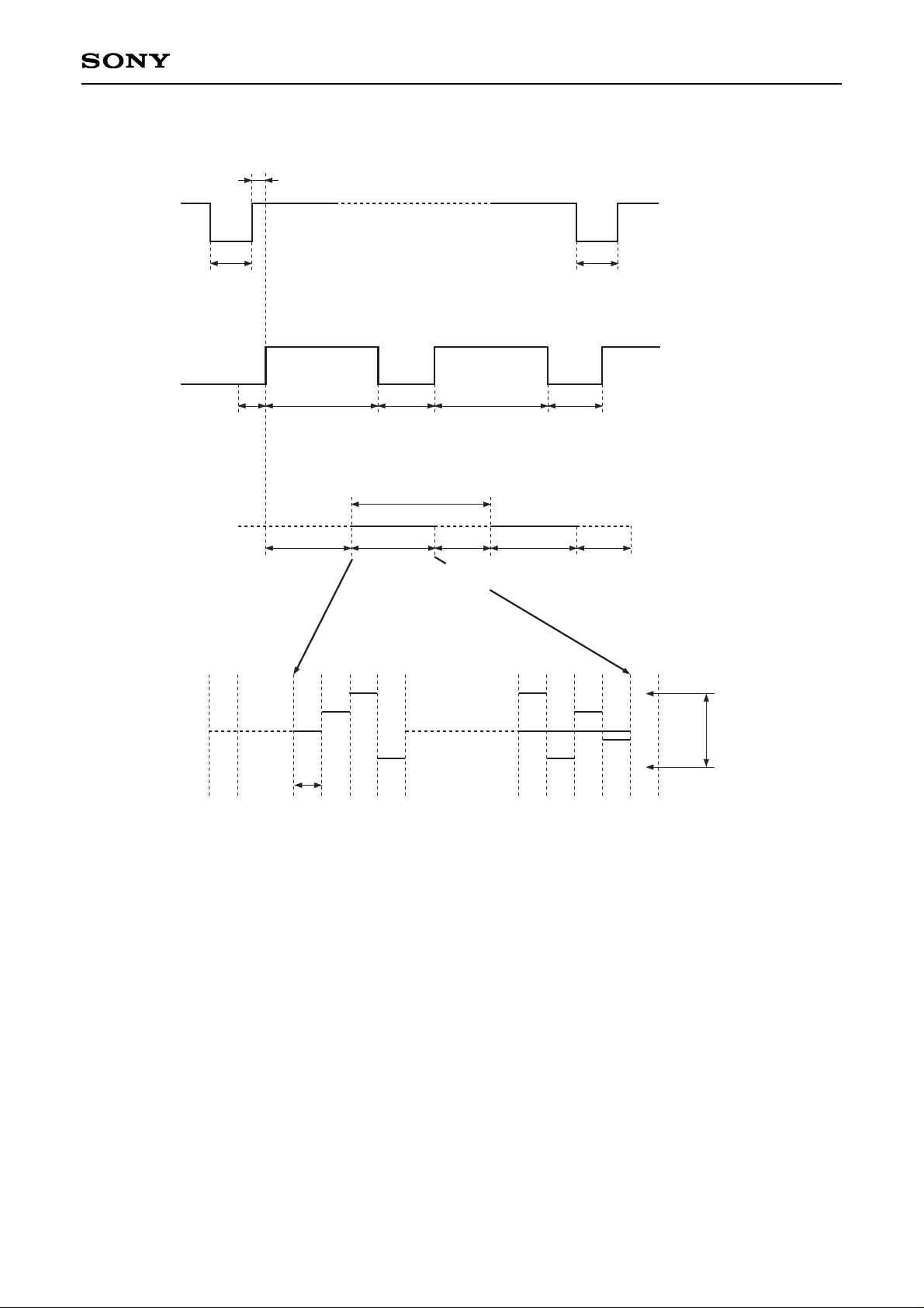
250ns
XSP
(3F)
Input
C_CK
(4E)
Output
AOUT
(7E)
Output
AOUT
(7E)
Detail
750ns
(Repeat 128 Times)
96.5µs
(193clk)
96µs
(192clk)
1st Culumn
32µs
(64clk)
96µs
(192clk)
2nd Culumn
32µs
(64clk)
D-range average
analog output
Analog output
Air level
0.6 to 1.3V
2.0V
0.6V
256.5µs
(513clk)
((192 + 1 + 63) × 2 + 1)
31.5µs
(63clk)
96.5µs
(193clk)
31.5µs
(63clk)
500ns
(1clk)
500ns
(1clk)
750ns
Page 17

– 17 –
CXA3271GE
Package Outline Unit: mm
SONY CODE
EIAJ CODE
JEDEC CODE
PACKAGE MATERIAL
TERMINAL TREATMENT
TERMINAL MATERIAL
PACKAGE MASS
ORGANIC SUBSTRATE
COPPER PLATING
LLGA-30P-01
GOLD PLATING
30PIN LLGA
0.7 g
PACKAGE STRUCTURE
52-φ1.2 ± 0.08
A
B
C
D
E
F
G
1 2 3
4 567
8
3-φ2.2
2.3
2.2
2.2
2.07
2.07
2.3
3.65
2.54
φ0.1
S
A B
M
2.54
3.42
B
A
X
0.25MAX
0.25MAX
DETAIL Y
TYP
TYP
SENSOR AREA
PIN1 INDEX
20
17
0.2
S A
M
0.15
0.2
S B
M
∗12.64 ± 0.25
∗2.6 ± 0.25
(10.04)
∗2.42 ± 0.25
(15.16)
Y
∗17.58 ± 0.25
4-R1.0MAX
(0.85)
DETAIL X
1.45 ± 0.2
0.05MAX
0.1
S
S
0.2 ± 0.2
NOTE2: The length of breedout is 0.25MAX.
breedout of sensor area.
NOTE1: Dimension “∗” does not include
Sony Corporation
 Loading...