

Page 1
Description
The CXA3106AQ is a PLL IC for LCD monitors/
projectors with built-in phase detector, charge pump,
VCO and counter.
The various internal settings are performed by
serial data via a 3-line bus.
Applicable LCD monitor/projector resolution are
NTSC, PAL, VGA, SVGA, XGA, and SXGA etc.
Features
• Supply voltage: 5V ± 10% single power supply
• Package: 48-pin QFP
• Power consumption: 350mW
• Sync input frequency: 10 to 100kHz
• Clock output signal frequency: 10 to 160MHz
• Clock delay: 1/16 to 20/16 CLK
• Sync delay: 1/16 to 20/16 CLK
• I/O level: TTL, PECL (complementary)
• Low clock jitter
• 1/2 clock output
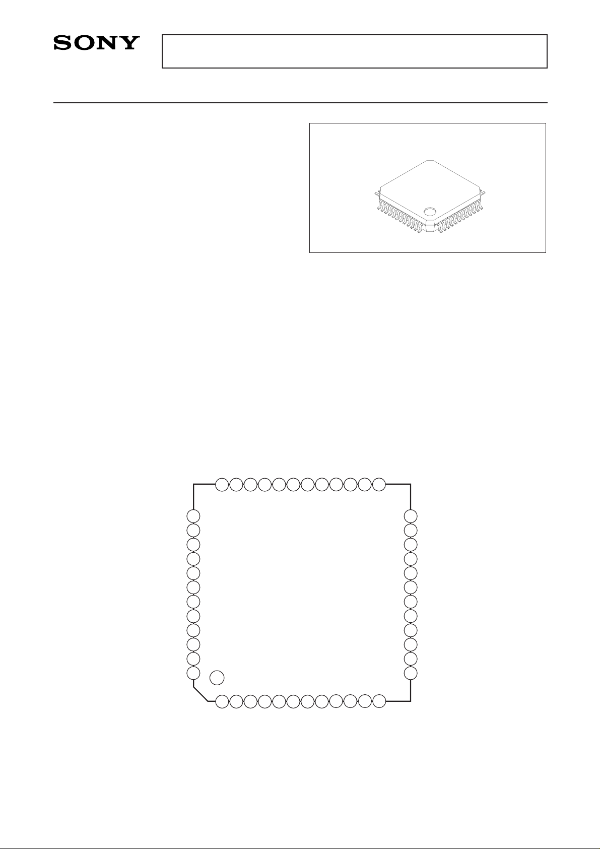
Pin Configuration (Top View)
Functions
• Phase detector enable
• UNLOCK output
• Output TTL disable function
• Power save function (2 steps)
Applications
• CRT displays
• LCD projectors
• LCD monitors
• Multi-media
– 1 –
CXA3106AQ
E97812A03
PLL IC for LCD Monitor/Projector
Sony reserves the right to change products and specifications without prior notice. This information does not convey any license by
any implication or otherwise under any patents or other right. Application circuits shown, if any, are typical examples illustrating the
operation of the devices. Sony cannot assume responsibility for any problems arising out of the use of these circuits.
48 pin QFP (Plastic)
13
14
15
16
17
18
19
20
21
22
23
24
25
26
27
28
29
30
36
35
34
31
32
33
40
39
38
37
41
42
43
44
45
46
47
48
IOV
CC
IOGND
VCOH
VCOL
VCO
HOLD
SYNCH
SYNCL
SYNC
SENABLE
SCLK
SDATA
PECLV
CC
VBB
DSYNCH
DSYNCL
CLKH
CLKL
CLK/2H
PECLV
CC
IOGND
TTLV
CC
TTLGND
IRVCC
IRGND
RC1
RC2
IREF
VCOHGND
VCOGND
VCOV
CC
PLLGND
PLLV
CC
IOVCC
IOGND
TLOAD
CS
SEROUT
DIVOUT
UNLOCK
DV
CC
DGND
CLK/2
CLKN
CLK
DSYNC
CLK/2L
CLK/2N
1
2
3
4
5
6
7
8
9
10
11
12
Page 2

– 2 –
CXA3106AQ
Absolute Maximum Ratings (Ta = 25°C)
• Supply voltage IOVCC, DVCC, TTLVCC, PECLVCC, PLLVCC,
VCOVCC, IRVCC, –0.5 to +7.0 V
IOGND, DGND, TTLGND, VCOHGND, PLLGND,
VCOGND, IRGND –0.5 to +0.5 V
• Input voltage VCOH, VCOL, SYNCH, SYNCL, VCO, HOLD,
SYNC, SENABLE, SCLK, SDATA, TLOAD, CS IOGND – 0.5 to IOVCC + 0.5 V
RC2 IRGND – 0.5 to IRVCC + 0.5 V
• Output current SEROUT, DIVOUT, UNLOCK, CLK/2N, CLK/2,
CLKN, CLK, DSYNC, CLK/2L, CLK/2H, CLKL,
CLKH, DSYNCH, DSYNCL, VBB –30 to +30 mA
IREF, RC1 –2 to +2 mA
• Storage temperature Tstg –65 to +150 °C
• Operating ambient temperature
Ta –25 to +75 °C
• Allowable power dissipation
PD 750 mW
Recommended Operating Conditions
Min. Typ. Max.
• Supply voltage IOVCC, DVCC, TTLVCC, PECLVCC,
PLLVCC, VCOVCC, IRVCC 4.75 5.00 5.25 V
IOGND, DGND, TTLGND, VCOHGND,
PLLGND, VCOGND, IRGND –0.05 0 0.05 V
• Digital input DIN (PECL) ∗1H level IOVCC – 1.1
DIN (PECL) ∗1L level IOVCC – 1.5 V
DIN (TTL) ∗2H level 2.0 V
DIN (TTL) ∗2L level 0.8 V
• SYNC, SYNCH, SYNCL input jitter 1.0 ns
• Operating temperature
Ta –20 +75 °C
∗1
VCOH, VCOL, SYNCH, SYNCL
∗2
VCO, HOLD, SYNC, SENABLE, SCLK, SDATA, TLOAD, CS
Page 3

– 3 –
CXA3106AQ
Block Diagram
TTLOUT
Polarity
Coarse
Delay
TTLOUT
TTLOUT
1bit
on/off
1bit
on/off
1bit
on/off
DSYNC
(TTL)
DSYNC
(PECL)
CLK
(TTL)
NCLK
(TTL)
CLK
(PECL)
TTLOUT
TTLOUT
1bit
on/off
1bit
on/off
CLK/2
(TTL)
NCLK/2
(TTL)
CLK/2
(PECL)
PECL
on/off
DIV1, 2, 4MUXVCO
Fine
Delay
Charge
Pump
Phase
Detector
PECLIN
TTLIN
PECLIN
TTLIN
Polarity
TTLIN
Programmable
Counter
whole chip
power save
synthesizer
power save
TTLINTTLOUTCONTROL REGISTERDAC
RESET
1/2
2bit
1bit5bit2bit
1bit
12bit
1/256 to 1/4096 CLK
1/16 to 20/16 CLK
1bit
1bit
1bit
CSTLOAD
DIVOUTSEROUT
SDATASCLKSENABLE
IREF
1bit2bit
Latch
logic
1bit
on/off
1bit
on/off
RC2RC1
VCO
(TTL)
VCO
(PECL)
SYNC
(TTL)
SYNC
(PECL)
HOLD
(TTL)
read out
TTLOUT
1 to 4 CLK
UNLOCK
VBB
PECLOUT
PECLOUT
PECLOUT
unlock
detect
Page 4

– 4 –
CXA3106AQ
Pin No. Symbol Description Reference voltage level
1 IOVCC Digital power supply 5V
2 IOGND Digital GND 0V
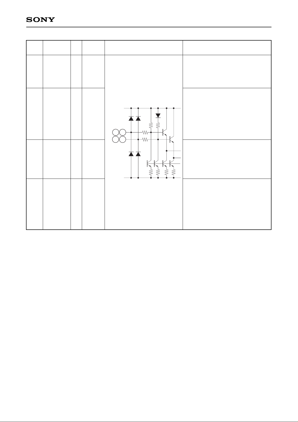
3 VCOH External VCO input PECL
4 VCOL External inverted VCO input PECL
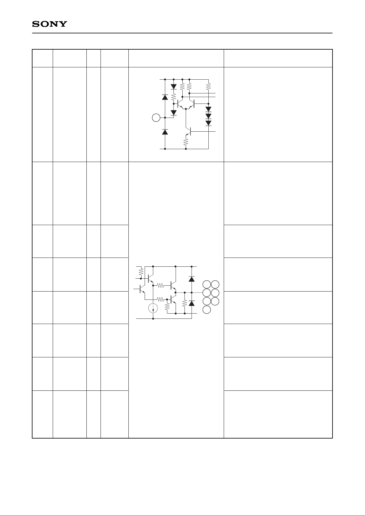
5 VCO External VCO input TTL
6 HOLD Phase detector disable signal input TTL
7 SYNCH Sync input PECL
8 SYNCL Inverted sync input PECL
9 SYNC Sync input TTL
10 SENABLE Control signal (enable) TTL
11 SCLK Control signal (clock) TTL
12 SDATA Control signal (data) TTL
13 TLOAD Programmable counter test input TTL
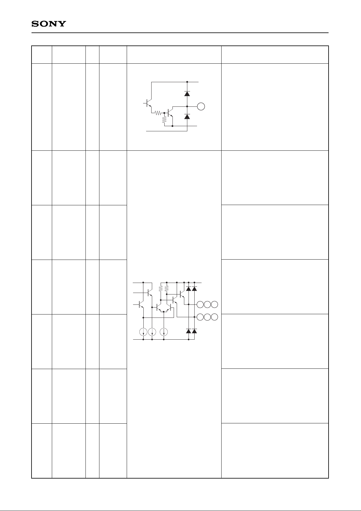
14 CS Chip select TTL
15 SEROUT Register read output TTL
16 DIVOUT Programmable counter test output TTL
17 UNLOCK Unlock signal output TTL
18 DVCC Digital power supply 5V
19 DGND Digital GND 0V
20 CLK/2N Inverted 1/2 clock output TTL
21 CLK/2 1/2 clock output TTL
22 CLKN Inverted clock output TTL
23 CLK Clock output TTL
24 DSYNC Delay sync signal output TTL
25 TTLGND TTL output GND 0V
26 TTLVCC TTL output power supply 5V
27 IOGND Digital GND 0V
28 PECLVCC PECL output power supply 5V
29 CLK/2L Inverted 1/2 clock output PECL
30 CLK/2H 1/2 clock output PECL
31 CLKL Inverted clock output PECL
32 CLKH Clock output PECL
33 DSYNCL Delay sync signal output PECL
34 DSYNCH Inverted delay sync signal output PECL
35 VBB PECL reference voltage PECLVCC – 1.3V
36 PECLVCC PECL output power supply 5V
37 IOGND Digital GND 0V
38 IOVCC Digital power supply 5V
39 PLLVCC PLL circuit analog power supply 5V
40 PLLGND PLL circuit analog GND 0V
41 VCOVCC VCO circuit analog power supply 5V
42 VCOGND VCO circuit analog GND 0V
43 VCOHGND VCO SUB analog GND 0V
44 IREF Charge pump current preparation 1.3V
45 RC2 External pin for LPF 1.7 to 4.4V
46 RC1 External pin for LPF 2.1V
47 IRGND IREF analog GND 0V
48 IRVCC IREF analog power supply 5V
Page 5

– 5 –
CXA3106AQ
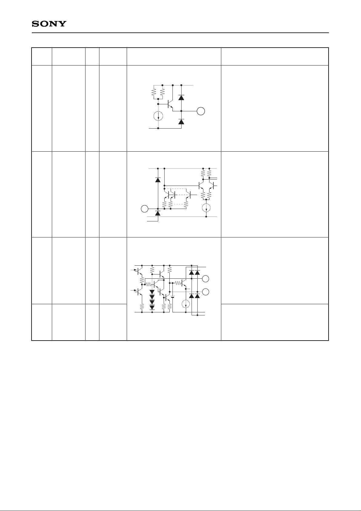
Pin Description and I/O Pin Equivalent Circuit
Digital power supply.
Ground this pin to the ground pattern
with a 0.1µF ceramic chip capacitor as
close to the pin as possible.
Digital GND.
Digital power supply.
Digital GND.
TTL output GND.
TTL output power supply.
Ground this pin to the ground pattern
with a 0.1µF ceramic chip capacitor as
close to the pin as possible.
Digital GND.
PECL output power supply.
Ground this pin to the ground pattern
with a 0.1µF ceramic chip capacitor as
close to the pin as possible.
PECL output power supply.
Ground this pin to the ground pattern
with a 0.1µF ceramic chip capacitor as
close to the pin as possible.
Digital GND.
Digital power supply.
Ground this pin to the ground pattern
with a 0.1µF ceramic chip capacitor as
close to the pin as possible.
PLL circuit analog power supply.
Ground this pin to the ground pattern
with a 0.1µF ceramic chip capacitor as
close to the pin as possible.
PLL circuit analog GND.
VCO circuit analog power supply.
Ground this pin to the ground pattern
with a 0.1µF ceramic chip capacitor as
close to the pin as possible.
VCO circuit analog GND.
VCO SUB analog GND.
IREF analog GND.
IREF analog power supply.
Ground this pin to the ground pattern
with a 0.1µF ceramic chip capacitor as
close to the pin as possible.
1
2
18
19
25
26
27
28
36
37
38
39
40
41
42
43
47
48
IOVCC
IOGND
DVCC
DGND
TTLGND
TTLVCC
IOGND
PECLVCC
PECLVCC
IOGND
IOVCC
PLLVCC
PLLGND
VCOVCC
VCOGND
VCOHGND
IRGND
IRVCC
5V
0V
5V
0V
0V
5V
0V
5V
5V
0V
5V
5V
0V
5V
0V
0V
0V
5V
—
—
—
—
—
—
—
—
—
—
—
—
—
—
—
—
—
—
Pin
No.
Symbol I/O
Reference
voltage level
Equivalent circuit Description
Page 6
– 6 –
CXA3106AQ
External VCO input.
Programmable counter test input
(switchable by a control register).
When using the VCO PECL input,
open the Pin 5 VCO TTL input.
External inverted VCO input.
When open, this pin goes to the PECL
threshold voltage (IOVcc – 1.3V).
Only the pin 3 VCOH input with VCOL
input open can be also operated but
complementary input is recommended
in order to realize stable high-speed
operation.
Sync input.
When using the SYNCH PECL input,
open the Pin 9 SYNC TTL input.
The sync signal can be switched
between positive/negative polarity by
an internal register.
Inverted sync input.
When open, this pin goes to the PECL
threshold voltage (IOVcc – 1.3V).
Only the Pin 7 SYNCH input with
SYNCL input open can be also
operated but complementary
input is recommended in order to
realize stable high-speed operation.
3
4
7
8
VCOH
VCOL
SYNCH
SYNCL
PECL
PECL
PECL
PECL
I
I
I
I
3
4
8
7
IOV
CC
IOGND
rr
Pin
No.
Symbol I/O
Reference
voltage level
Equivalent circuit Description
Page 7

– 7 –
CXA3106AQ
External VCO input.
Programmable counter test input
(controlled by a control register).
When using the VCO TTL input, open
the Pin 3 VCOH and Pin 4 VCOL
PECL inputs.
Phase detector disable signal.
Active high. When this pin is high, the
phase detector output is held. This pin
goes to high level when open.
(See the HOLD Timing Chart.)
Sync input.
When using the SYNC TTL input,
open the Pin 7 SYNCH and Pin 8
SYNCL PECL inputs.
The sync signal can be switched
between positive/negative polarity by
a control register.
Control signal (enable) for setting the
internal registers.
When SENABLE is low, registers can
be written; when high, registers can be
read.
(See the Control Register Table and
Control Timing Chart.)
Control signal (clock) for setting the
internal registers.
When SENABLE is low, SDATA is
loaded to the registers at the rising
edge of SCLK.
When SENABLE is high, the register
contents are output from SEROUT at
the falling edge of SCLK.
(See the Control Register Table and
Control Timing Chart.)
Control signal (data) for setting the
internal registers.
(See the Control Register Table and
Control Timing Chart.)
Programmable counter test input.
This pin is normally open status and
high. Register contents can be loaded
immediately to Programmable counter
by setting TLOAD low during the
programmable counter test mode.
5
6
9
10
11
12
13
VCO
HOLD
SYNC
SENABLE
SCLK
SDATA
TLOAD
TTL
TTL
TTL
TTL
TTL
TTL
TTL
I
I
I
I
I
I
I
5
6
9
10
12
13
r/2
r
2r
1.5V
IOVCC
IOGND
11
Pin
No.
Symbol I/O
Reference
voltage level
Equivalent circuit Description
Page 8
– 8 –
CXA3106AQ
Chip select.
When low, all circuits including the
register circuit are set to the power
save mode.
When high, all circuits are set to
operating mode.
Register read output.
When SENABLE is high, the register
contents are output from SEROUT at
the falling edge of SCLK.
(See the Control Register Timing
Chart.)
TTL output can be turned ON/OFF
(high impedance) by a control register.
Programmable counter test output.
(See the I/O Timing Chart.)
TTL output can be turned ON/OFF
(high impedance) by a control register.
Inverted 1/2 clock output.
(See the I/O Timing Chart.)
TTL output can be turned ON/OFF
(high impedance) by a control register.
1/2 clock output.
(See the I/O Timing Chart.)
TTL output can be turned ON/OFF
(high impedance) by a control register.
Inverted clock output.
(See the I/O Timing Chart.)
TTL output can be turned ON/OFF
(high impedance) by a control register.
Clock output.
(See the I/O Timing Chart.)
TTL output can be turned ON/OFF
(high impedance) by a control register.
Delay sync signal output.
(See the I/O Timing Chart.)
TTL output can be turned ON/OFF
(high impedance) and switched
between positive/negative polarity by
a control register.
14
15
16
20
21
22
23
24
CS
SEROUT
DIVOUT
CLK/2N
CLK/2
CLKN
CLK
DSYNC
TTL
TTL
TTL
TTL
TTL
TTL
TTL
TTL
I
O
O
O
O
O
O
O
IOVCC
IOGND
14
IOVCC
IOGND
TTLV
CC
TTLGND
15
20
21
22
23
24
16
100k
Pin
No.
Symbol I/O
Reference
voltage level
Equivalent circuit Description
Page 9
– 9 –
CXA3106AQ
Unlock signal output.
This pin is an open collector output,
and pulls in the current when a phase
difference occurs. The UNLOCK
sensitivity can be adjusted by
connecting a capacitor and resistors
to this output as appropriate.
(See the UNLOCK Timing Chart.)
TTL output can be turned ON/OFF
(high impedance) by a control register.
Inverted 1/2 clock output.
(See the I/O Timing Chart.)
This pin requires an external pulldown resistor.
When not used, connect to PECLVCC
without connecting a pull-down
resistor.
1/2 clock output.
(See the I/O Timing Chart.)
This pin requires an external pulldown resistor.
When not used, connect to PECLVCC
without connecting a pull-down
resistor.
Inverted clock output.
(See the I/O Timing Chart.)
This pin requires an external pulldown resistor.
When not used, connect to PECLVCC
without connecting a pull-down
resistor.
Clock output.
(See the I/O Timing Chart.)
This pin requires an external pulldown resistor.
When not used, connect to PECLVCC
without connecting a pull-down
resistor.
Delay sync signal output.
(See the I/O Timing Chart.)
This pin requires an external pulldown resistor.
When not used, connect to PECLVCC
without connecting a pull-down
resistor.
Inverted delay sync signal output.
(See the I/O Timing Chart.)
This pin requires an external pulldown resistor.
When not used, connect to PECLVCC
without connecting a pull-down
resistor.
17
29
30
31
32
33
34
UNLOCK
CLK/2L
CLK/2H
CLKL
CLKH
DSYNCL
DSYNCH
TTL
PECL
PECL
PECL
PECL
PECL
PECL
O
O
O
O
O
O
O
17
TTLVCC
IOGND
TTLGND
IOGND
IOVCC
29
30
34
31
32
33
PECLV
CC
Pin
No.
Symbol I/O
Reference
voltage level
Equivalent circuit Description
Page 10
– 10 –
CXA3106AQ
PECL reference voltage.
When used, ground this pin to the
ground pattern with a 0.1µF ceramic
chip capacitor as close to the pin as
possible.
Charge pump current preparation.
Connect to GND via an external
resistor (1.6kΩ).
Ground this pin to the ground pattern
with a 0.1µF ceramic chip capacitor
as close to the pin as possible.
External pin for LPF.
See the Recommended Operating
Circuit for the external circuits. Note
that external resistors and capacitors
should be metal film resistors and
temperature compensation capacitors
which are relatively unaffected by
temperature change.
External pin for LPF.
See the Recommended Operating
Circuit for the external circuits.
VBB
IREF
RC2
RC1
O
O
O
O
PECLVCC
–1.3V
1.3V
1.7
to
4.4V
2.1V
35
44
45
46
Pin
No.
Symbol I/O
Reference
voltage level
Equivalent circuit Description
PECLVCC
IOGND
35
IRVCC
IRGND
44
IOGND
VCOVCC
VCOGND
IOGND
IRGND
IRV
CC
45
46
100
Page 11

– 11 –
CXA3106AQ
Control Register Table
Register No.
Register 1
Register 2
Register 3
Register 4
Register 5
Register 6
Register 7
Register Name
register read no
DIVREG1
register read no
DIVREG2
register read no
CENFREREG
register read no
DELAYREG
register read no
CPREG
register read no
TTLPOLREG
register read no
TESTPOWREG
DATA7
MSB1VCO
DIV
Bit 7
30
UNLOCK
Enable
DAT6
2
VCO
DIV
Bit 6
13
DIV 1, 2, 4
Bit 1
20
COARSE
DELAY
Bit 1
31
DSYNC
Enable
DATA5
3
VCO
DIV
Bit 5
14
DIV 1, 2, 4
Bit 0
21
COARSE
DELAY
Bit 0
32
NCLK/2
Enable
DATA4
4
VCO
DIV
Bit 4
15
N/A
∗
1
22
FINE
DELAY
Bit 4
33
CLK/2
Enable
DATA3
5
VCO
DIV
Bit 3
9
VCO
DIV
Bit 1116N/A
∗1
23
FINE
DELAY
Bit 3
34
NCLK
Enable
38
DIVOUT
Enable
DATA2
6
VCO
DIV
Bit 2
10
VCO
DIV
Bit 1017N/A
∗
1
24
FINE
DELAY
Bit 2
27
PD
POL
35
CLK
Enable
39
Read out
power
DATA1
7
VCO
DIV
Bit 1
11
VCO
DIV
Bit 9
18
N/A
∗
1
25
FINE
DELAY
Bit 1
28
C.Pump
Bit 1
36
DSYNC
POL
40
Synth
power
DATA0
8
VCO
DIV
Bit 0
12
VCO
DIV
Bit 8
19
N/A
∗
1
26
FINE
DELAY
Bit 0
29
C.Pump
Bit 0
37
SYNC
POL
41
VCO
By-pass
∗2
ADDR2
MSB
0
0
0
1
1
1
1
ADDR1
0
1
1
0
0
1
1
ADDR0
LSB
1
0
1
0
1
0
1
DATA ADDRESS
∗
1
Register read no. 15 to 19 are N/A.
∗2
VCO By-pass at register read no. 41 is a MUX control bit in Block Diagram.
Page 12

– 12 –
CXA3106AQ
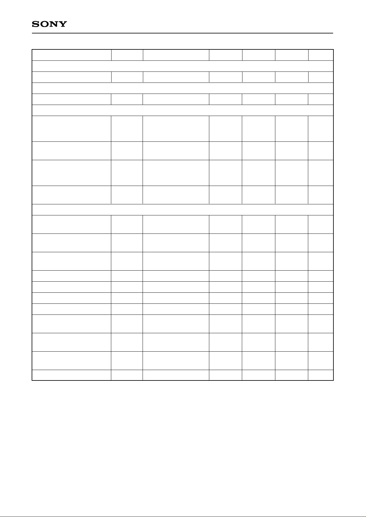
Electrical Characteristics (Ta = 25°C, VCC = 5V, GND = 0V)
Current consumption (excluding output current)
Current consumption 1
Current consumption 2
Current consumption 3
Digital input
Digital high level input
voltage (PECL)
Digital low level input
voltage (PECL)
VCOL, SYNCL input open
voltage (PECL)
Digital high level input
current (PECL)
Digital low level input
current (PECL)
Digital high level input
voltage (TTL)
Digital low level input
voltage (TTL)
Digital high level input
current (TTL)
Digital low level input
current (TTL)
HOLD characteristics
RC1 input pin leak current
HOLD signal set-up time
HOLD signal hold time
Digital output
Digital high level output
voltage (PECL)
Digital low level output
voltage (PECL)
PECL output reference
voltage
Digital high level output
voltage (TTL)
Digital low level output
voltage (TTL)
CS = H, Synth Power = 1
CS = H, Synth Power = 0
CS = L
VIH = IOVCC – 0.8V
VIL = IOVCC – 1.6V
VIH = 2.7V
VIL = 0.5V
RL = 330Ω
RL = 330Ω
RL = 330Ω
CL = 10pF
CL = 10pF
40
5
3
IOVCC
–1.15
–100
–200
2.0
–200
–500
20
20
PECLVCC
–1.1
2.7
70
19
14
IOVCC
–1.3
PECLVCC
–1.3
105
38
24
IOVCC
–1.5
100
0
0.8
–20
–100
1.0
PECLVCC
–1.6
0.5
mA
mA
mA
V
V
V
µA
µA
V
V
µA
µA
nA
ns
ns
V
V
V
V
V
ICC1
ICC2
ICC3
VIH1
VIL1
VIO
IIH1
IIL1
VIH2
VIL2
IIH2
IIL2
Ileak
Ths
Thh
VOH1
VOL1
VBB
VOH2
VOL2
Item Symbol Conditions Min. Typ. Max. Unit
Page 13
– 13 –
CXA3106AQ
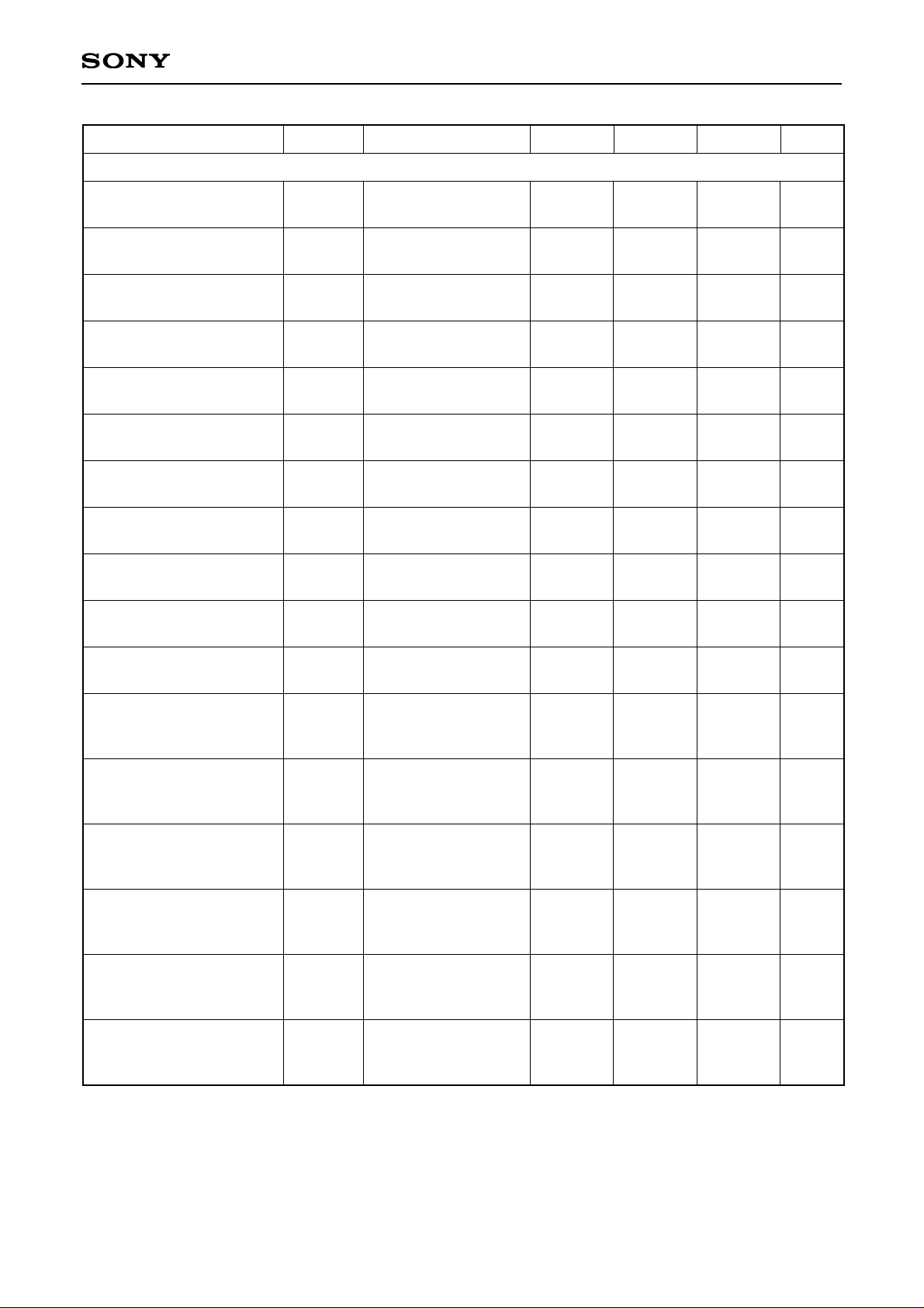
UNLOCK output
UNLOCK output current
SYNC input
SYNC input frequency range
DSYNC output
DSYNC output variable
coarse delay time setting
resolution
DSYNC output variable
coarse delay time
DSYNC output variable
fine delay time setting
resolution
DSYNC output variable
fine delay time
VCO characteristics
DIV output frequency
operation range 1
DIV output frequency
operation range 2
DIV output frequency
operation range 3
VCO lock range
VCO gain 1
VCO gain 2
VCO gain 3
Charge pump current 1
Charge pump current 2
Charge pump current 3
VCO counter bits
DIV = 1/1
DIV = 1/2
DIV = 1/4
DIV = 1/1
DIV = 1/2
DIV = 1/4
C.Pump Bit = 00,
IREF = 1.6kΩ
C.Pump Bit = 10,
IREF = 1.6kΩ
C.Pump Bit = 11,
IREF = 1.6kΩ
–30
10
1
1/16
40
20
10
1.7
240
120
60
80
350
1350
2
5
400
200
100
100
400
1600
12
100
4
20/16
160
80
40
4.4
640
320
160
130
500
1800
mA
kHz
bit
CLK
bit
CLK
MHz
MHz
MHz
V
Mrad/sv
Mrad/sv
Mrad/sv
µA
µA
µA
bit
Iunlock
Fin
Rdsync1
Td1
Rdsync2
Td2
FVCO1
FVCO2
FVCO3
Vlock
KVCO1
KVCO2
KVCO3
Kpd1
Kpd2
Kpd3
Rdiv2
Item Symbol Conditions Min. Typ. Max. Unit
Page 14
– 14 –
CXA3106AQ
CLK (CLK, CLK/2) output
CLK output (PECL)
frequency range 1
CLK output (PECL)
frequency range 2
CLK output (PECL)
frequency range 3
CLK, CLK/2 output (PECL)
rise time
CLK, CLK/2 output (PECL)
fall time
CLK output (TTL)
frequency range 1
CLK output (TTL)
frequency range 2
CLK output (TTL)
frequency range 3
CLK, CLK/2 output (TTL)
rise time
CLK, CLK/2 output (TTL)
fall time
CLK output (PECL, TTL)
duty
SYNC input (PECL) and
CLK output (PECL) delay
offset
CLK output (PECL) and
DSYNC output (PECL)
phase difference
CLK output (PECL) and
CLK/2 output (PECL)
phase difference
CLK output (PECL) and
DIVOUT output (TTL) rise
phase difference
CLK output (PECL) and
DIVOUT output (TTL) fall
phase difference
DSYNC, CLK, CLK/2 PECL
output and TTL output
phase difference
DIV = 1/1
DIV = 1/2
DIV = 1/4
10% to 90%,
RL = 330Ω
10% to 90%,
RL = 330Ω
DIV = 1/1
DIV = 1/2
DIV = 1/4
10% to 90%,
CL = 10pF
10% to 90%,
CL = 10pF
CL = 10pF
CL = 10pF
CL = 10pF
CL = 10pF
CL = 10pF
CL = 10pF
CL = 10pF
40
20
10
1.0
1.0
40
20
10
2.0
2.0
40
1.5
0.0
10
8
1.5
1.5
1.5
3.0
3.0
50
1
2.4
0.8
14
11
3.0
160
80
40
2.0
2.0
80
80
40
4.0
4.0
60
3.0
1.0
19
14
4.5
MHz
MHz
MHz
ns
ns
MHz
MHz
MHz
ns
ns
%
ns
ns
ns
ns
ns
ns
Fclk1PECL
Fclk2PECL
Fclk3PECL
TrPECL
TfPECL
Fclk1TTL
Fclk2TTL
Fclk3TTL
TrTTL
TfTTL
Dclk2
Td3
Td4
Td5
Td6
Td7
Td8
Item Symbol Conditions Min. Typ. Max. Unit
Page 15

– 15 –
CXA3106AQ
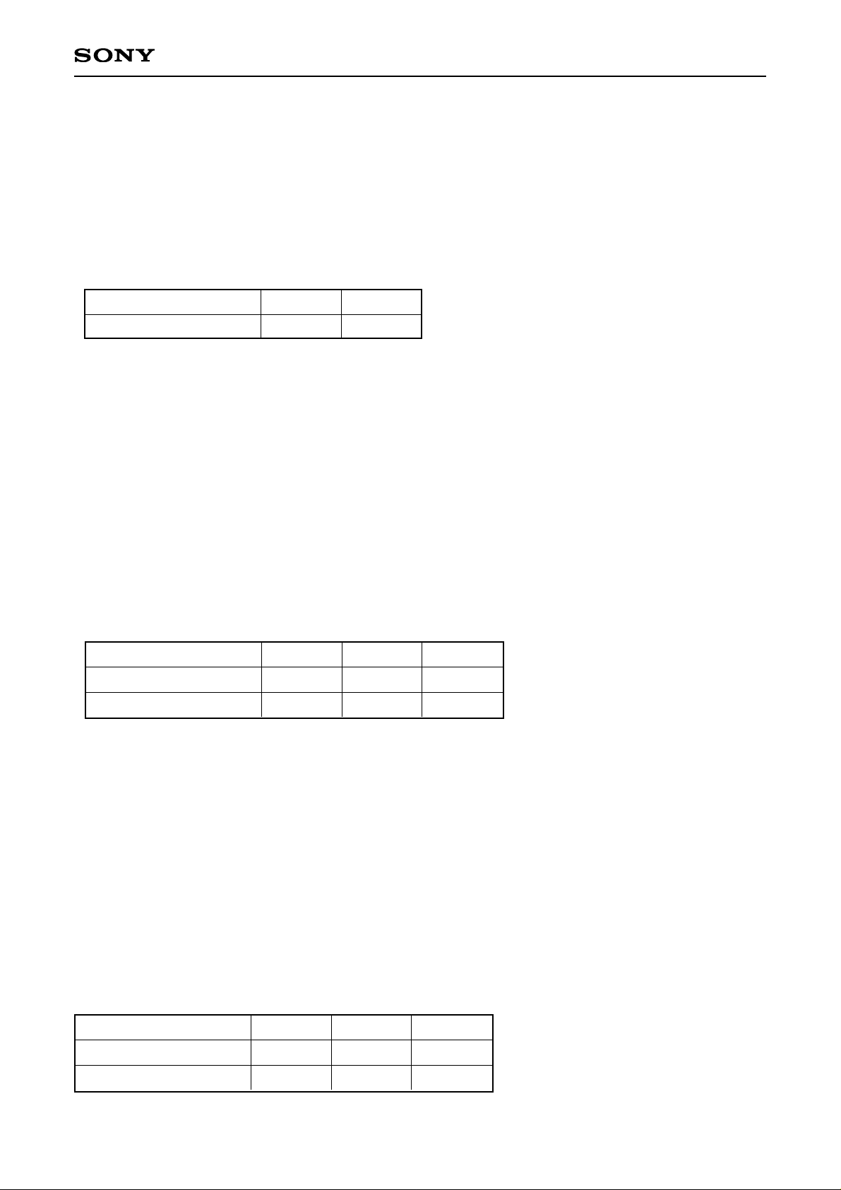
CLK (CLK, CLK/2) output
CLK vs. SYNC output jitter
(NTSC)
CLK vs. SYNC output jitter
(VGA)
CLK vs. SYNC output jitter
(SVGA)
CLK vs. SYNC output jitter
(XGA)
CLK vs. SYNC output jitter
(SXGA)
CLK vs. DSYNC output jitter
Control registers
SCLK frequency
SENABLE setup time
SENABLE hold time
SDATA setup time
SDATA hold time
SENABLE setup time
SENABLE hold time
triggered at SYNC
Fsync = 15.73kHz
(Crystal)
Fclk = 12.27MHz
N = 780
triggered at SYNC
Fsync = 31.47kHz
(Crystal)
Fclk = 25.18MHz
N = 800
triggered at SYNC
Fsync = 48.08kHz
(Crystal)
Fclk = 50.00MHz
N = 1040
triggered at SYNC
Fsync = 56.48kHz
(Crystal)
Fclk = 75.00MHz
N = 1328
triggered at SYNC
Fsync = 80kHz
(Crystal)
Fclk = 136.00MHz
N = 1700
triggered at DSYNC
in write/read mode
in write mode
in write mode
in write mode
in read mode
in read mode
in read mode
3.0
1.0
0.9
0.8
0.6
3
0
3
0
3
0
5.0
2.0
1.6
1.5
1.0
8.0
3.0
2.5
2.0
1.4
0.1
12
ns
ns
ns
ns
ns
ns
MHz
ns
ns
ns
ns
ns
ns
Tj1p-p
Tj2p-p
Tj3p-p
Tj4p-p
Tj5p-p
Tj6p-p
SCLK
TENS
TENH
TDS
TDH
TNENS
TNENH
Item Symbol Conditions Min. Typ. Max. Unit
Page 16
– 16 –
CXA3106AQ
Description of Block Diagram
Sync Input
Sync signals in the range of 10 to 100kHz can be input. Input supports both positive and negative polarity.
PECL input can also be a single input.
When SYNC is positive polarity, the clock is regenerated in synchronization with the rising edge of the sync signal.
When SYNC is negative polarity, the clock is regenerated in synchronization with the falling edge of the sync signal.
VCO oscillation stops when there is no sync input.
Register: SYNC POL
SYNC input polarity
1
Positive
0
Negative
Phase Detector
The phase detector operates at the sync input frequency of 10 to 100kHz. The PD input polarity should be
set to the default PD POL = 1. Phase comparison is performed at the edges.
The input circuit of the phase detector does not contain a hysteresis circuit, so the waveform must be shaped
at the front end of the CXA3106AQ when inputting a noisy signal.
The phase detector HOLD signal is supplied by TTL. (See the HOLD Timing Chart.)
The PLL UNLOCK signal is output by an open collector.
(See the UNLOCK Timing Chart.)
Charge Pump
The gain (I, I/4, I/16) can be varied by changing the charge pump current using 2 bits of control register.
Register: C.Pump bit 1
Register: C.Pump bit 0
0
0
1
0
1
1
Charge pump current
100µA
400µA 1600µA
Register: DIV 1, 2, 4 bit 1
Register: DIV 1, 2, 4 bit 0
0
0
1
0
1
1
Counter frequency divisions
1/1
1/2 1/4
LPF
This is a loop filter comprised of the external capacitors and resistor.
Be sure to use metal film resistors with little temperature variation and a temperature-compensated capacitor.
In particular, the 0.33µF capacitor should be equivalent to high dielectric constant series capacitor type B or
better. (electrostatic capacitance change ratio ±10%: T = –25 to +85°C)
VCO
The VCO oscillator frequency covers from 40 to 160MHz.
VCO Rear-end Counter
The VCO output is frequency divided to 1/1, 1/2 or 1/4 by switching 2 bits of control register.
The operating range can be expanded to 10 to 160MHz by combining the counter with a VCO frequency divider.
Page 17

– 17 –
CXA3106AQ
Feedback Programmable Counter
This counter can be set as desired from 256 to 4096 using 12 bits.
Frequency divisions = (m + 1) × 8 + n, n: 3 bits (VCO DIV bits 0 to 2), m: 9 bits (VCO DIV bits 3 to 11)
When the register value is changed, the new setting is actually loaded to the counter when the counter value
becomes "all 0".
Clock Output
When SYNC input is positive polarity, the clock is regenerated in synchronization with the rising edge of the
sync signal.
The clock output delay time can be changed in the range of 1/16 to 20/16 CLK using 5 bits of control register.
(See the I/O Timing Chart.)
Output is TTL and PECL (complementary), and supports both positive and negative polarity. Clock TTL
output can also be turned off independently.
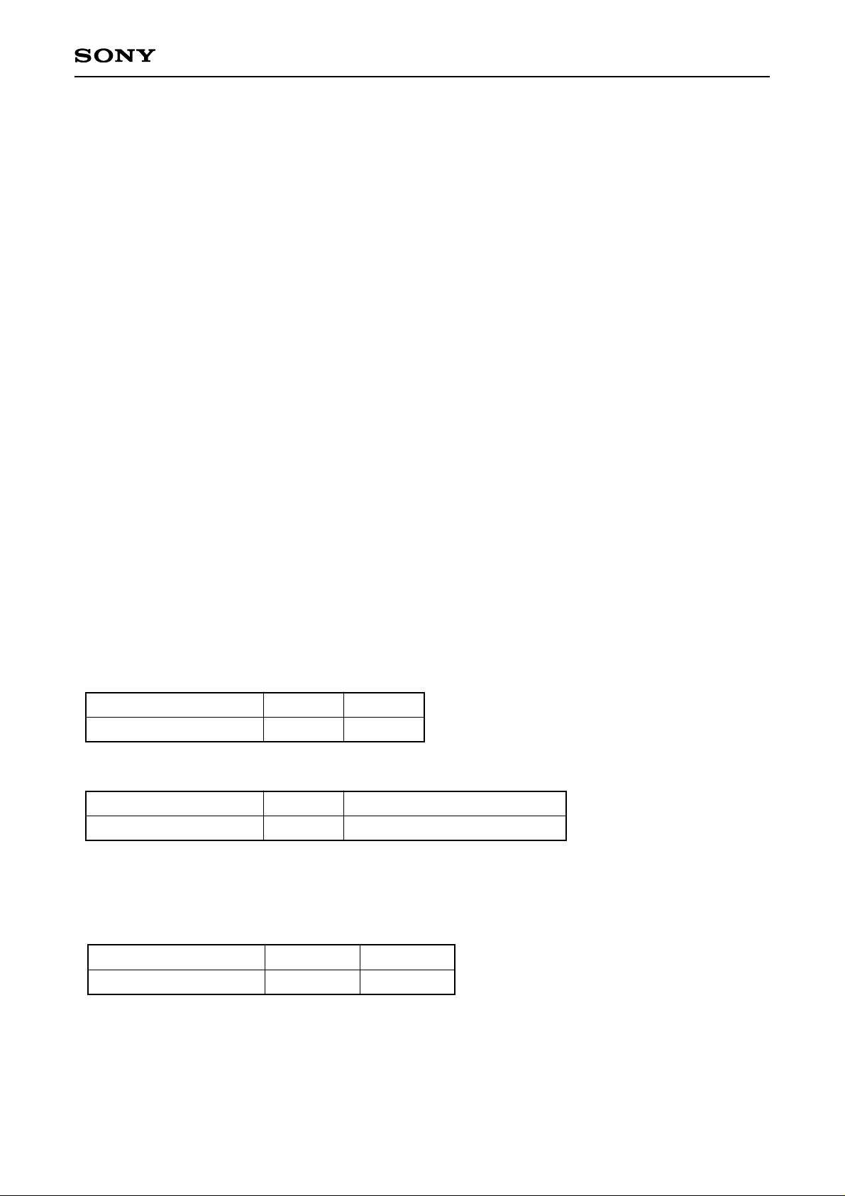
Register: Clock Enable
Clock output status
1
ON
0
OFF
Register: Clock Enable
Clock output status
1
ON
0
OFF
Register: DSYNC POL
DSYNC output polarity
1
Positive
0
Negative
Lower delay line
FINE DELAY bits 0 to 4
Delay time
00000
1/16CLK
00001
2/16CLK
· · · · · · · · · · · ·
· · · · · · · · · · · ·
10011
20/16CLK
Upper delay line
COARSE DELAY bits 0 to 1
Delay time
00
1CLK
01
2CLK
10
3CLK
11
4CLK
Delay Sync Output
The front edge of the delay sync pulse is latched by the pulse obtained by frequency dividing the CLK
regenerated by the PLL, so there is almost no jitter with respect to CLK. This front edge can be used as the
reset signal for the system timing circuit.
The rear edge of the delay sync pulse is latched by the CLK regenerated by the PLL. This relationship is
undefined for one clock as shown in the Timing Chart.
The delay sync output delay time can be varied in two stages. First, the delay time can be varied in the range
of 1/16 to 20/16 CLK using 5 bits of control register, and then in the range of 1 to 4 CLK using 2 bits of
control register. In other words, the total delay time is ((1/16 to 20/16) + (1 to 4)) CLK. (See the I/O Timing
Chart.)
DSYNC output is TTL and PECL (complementary), and supports both positive and negative polarity. Clock
TTL output can also be turned off.
1/2 Clock Output
Reset is performed at the delay sync timing and the clock output is frequency divided by 1/2. (See the I/O
Timing Chart.)
Both odd and even output are TTL and PECL output. TTL output can also be turned off independently.
Register: Clock Enable
Clock output status
1
ON
0
OFF
Page 18
– 18 –
CXA3106AQ
Control Circuit (3-bit address, 8-bit data)
The timing and input methods are described hereafter.
Feedback programmable counter control REGISTER1, 2 12bit VCO DIV Bit0 to 11
VCO rear-end counter control REGISTER3 2bit DIV1, 2, 4 Bit0, Bit1
Fine delay line control REGISTER4 5bit FINE DELAY Bit0 to 4
Coarse delay line control REGISTER4 2bit COARSE DELAY Bit0, Bit1
Charge pump current DAC control REGISTER5 2bit C.Pump Bit0, Bit1
Phase detector input positive/negative polarity control REGISTER5 1bit PD POL
Sync input positive/negative polarity control REGISTER6 1bit SYNC POL
Delay sync output positive/negative polarity control REGISTER6 1bit DSYNC POL
Clock TTL output OFF function REGISTER6 1bit CLK Enable
Inverted clock TTL output OFF function REGISTER6 1bit NCLK Enable
1/2 clock TTL output OFF function REGISTER6 1bit CLK/2 Enable
Inverted 1/2 clock TTL output OFF function REGISTER6 1bit NCLK/2 Enable
Delay sync TTL output OFF function REGISTER6 1bit DSYNC Enable
UNLOCK output OFF function REGISTER6 1bit UNLOCK Enable
Programmable counter input switching REGISTER7 1bit VCO By-pass
Power save with register contents held REGISTER7 1bit Synth power
Register read function power ON/OFF REGISTER7 1bit Read out power
Programmable counter TTL output OFF function REGISTER7 1bit DIVOUT Enable
Power Save
The CXA3106Q realizes 2-step power saving (all OFF, control registers only ON). This is controlled by a
control register and the chip selector.
Step 1: Chip selector control
CS
Power save status
H
Power ON
L
All OFF
Register: Synth power
Power save status
1
Power ON
0
Control registers only ON
Step 2: Control register control
Readout Circuit (during test mode)
The control register contents can be read by serial data from SEROUT.
(See the Control Register Timing Chart.)
Register: Read out power
Readout status
0
Function OFF
1
Function ON
Page 19
– 19 –
CXA3106AQ
Register: DIVOUT Enable
DIVOUT output status
0
OFF
1
ON
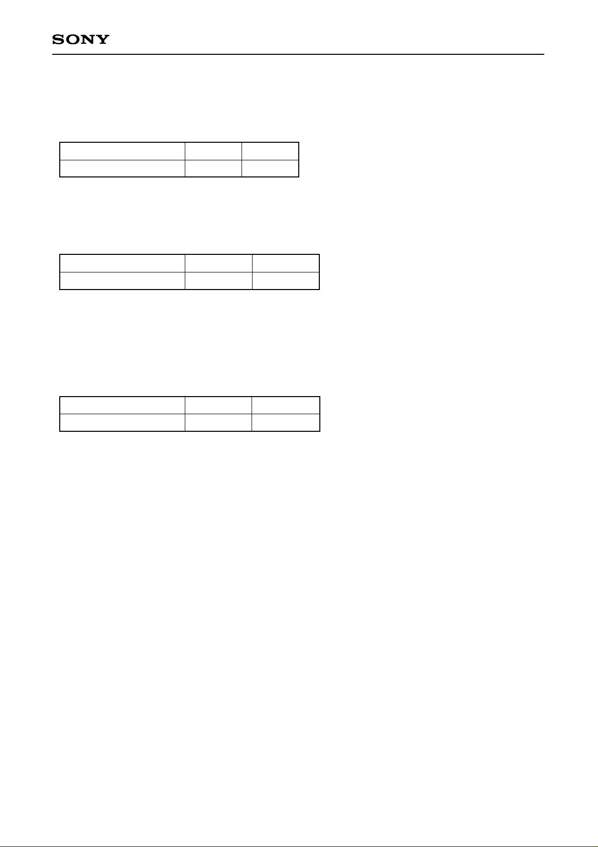
Register: VCO By-pass
Input status
1
Internal VCO
0
External input
TLOAD
Forced load control status
H
Function OFF
L
Function ON
Programmable Counter Output (during test mode)
The programmable counter output is TTL output from the DIVOUT pin.
(See the I/O Timing Chart.)
This output is normally not used.
TLOAD input (during test mode)
This control signal forcibly loads the control register contents to the programmable counter.
This signal is normally not used.
VCO input (during test mode)
This is the programmable counter test signal input pin.
This pin can be switched internally by the MUX circuit.
TTL and PECL input are possible.
This pin is normally not used.
Page 20
– 20 –
CXA3106AQ
Control Register Timing
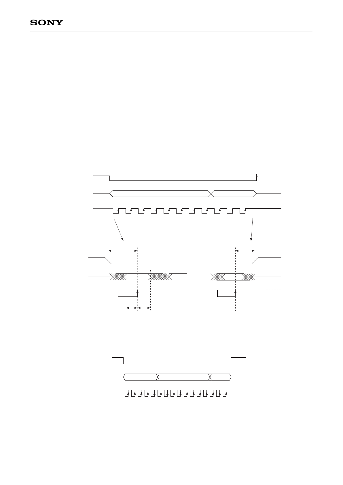
1) Write mode
Many CXA3106AQ functions can be controlled via a program. Characteristics are changed by setting the
internal control register values via a serial interface comprised of three pins: SENABLE (Pin 10), SCLK (Pin
11) and SDATA (Pin 12). The write timing diagram is shown below.
Input the 8-bit data and 3-bit register address MSB first to the SDATA pin. Some registers are not 8 bits, but
the data is input aligned with the LSB side in these cases. (See the Register Table.)
SENABLE is the enable signal and is active low. SCLK is the transfer clock signal, and data is loaded to the
IC at the rising edge. When SENABLE rises, SCLK must be high. (Registers are set at the rising edge of
SENABLE.) When SENABLE falls, SCLK may be either high or low.
SENABLE
SDATA
SCLK
SENABLE
SDATA
SCLK
DATA
8bit
ADDRESS
3bit
Enlarged
TENS TENH
TDHTDS
Enlarged
For example, when inputting a 16-bit signal, the initial 5 bits are invalid and the latter 11 bits are valid. This is
to say that the latter 11 bits are loaded to the register.
SENABLE
SDATA
SCLK
DATA
8bit
address
3bit
Invalid DATA
5bit
Page 21
– 21 –
CXA3106AQ
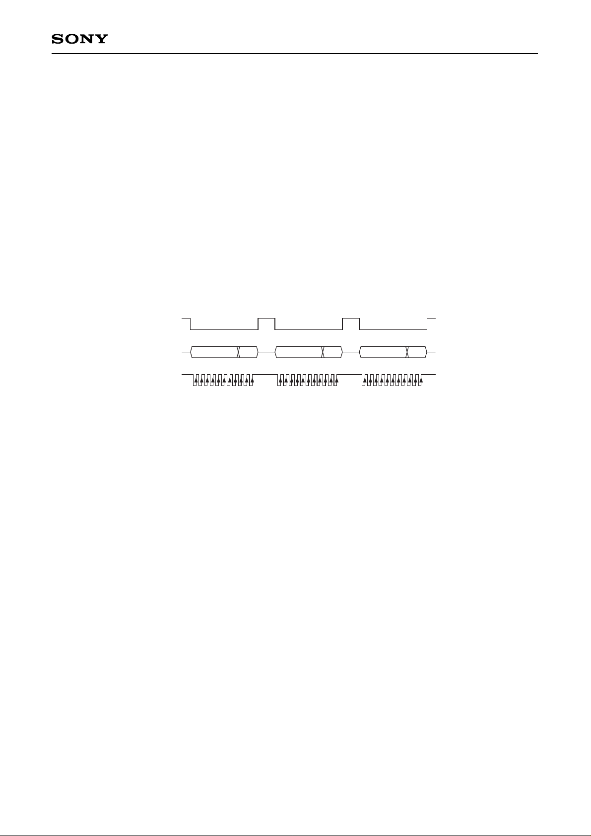
The settings of the frequency divider (2 bits, DIV1, 2, 4) and programmable counter (12 bits, VCODIV) at the
rear end of the VCO are transferred in the order shown below. (The data will be set when the three registers
are transferred.)
First DIVREG2, CENFREREG and DIVREG1 are set, and then the data is transferred independently at the
timings shown below.
DIVREG2 (upper 4 bits of VCODIV)
↓
CENFREREG (2 bits of DIV1, 2, 4)
↓
DIVREG1 (lower 8 bits of VCODIV)
All three of the above registers must be changed even when changing only DIV1, 2, 4 (2 bits). This is the
same when changing only VCODIV (12 bits).
SENABLE
SDATA
SCLK
DIVREG2
CENFREREG DIVREG1
Page 22

– 22 –
CXA3106AQ
2) Read mode
Data can be transferred from the shift register to the data register only when SENABLE is high.
Binary data can be read from the data register by inputting SCLK when SENABLE is high. Data is loaded
from the data register to the SCAN PATH circuit each time one clock is input to SCLK, and is output
sequentially from the register read no. 1 data (VCODIV bit 7) through the SEROUT pin. When the 41st SCLK
clock pulse is input, the register read no. 41 data (VCO By-pass) is output. Then, when the 42nd clock pulse
is input to SCLK, the output returns to the register read no. 1 data (VCODIV bit 7) and the data output is
repeated. Also, the data output from the SCAN PATH circuit is automatically reloaded even when the shift
register data is changed during data output.
Note) Since all registers do not have 8 bits, only the valid bits of each register are loaded to the SCAN PATH
circuit. (See the Control Register Table for the actual register read no.)
SEROUT
I/P SHIFT REGISTER, 11 BITS
8 BIT DATA 3 BIT ADDRESS
CLK
NEN
TR
EN
CLK
SCLK
SENABLE
7 DATA REGISTERS (41 LATCHES).
REGISTERS ARE DIFFERENT LENGTHS
UP TO 8 BIT
SCAN PATH, 1 ELEMENT PER REGISTER BIT
TNENS TNENH
READ NO. 1 READ NO. 2 READ NO. N
N
1 2
SENA
SEROUT
SCLK
Block Diagram during Read Mode
Timing Chart during Read Mode
Page 23

– 23 –
CXA3106AQ
Timing Charts
1. I/O timing
0 1 2 3 4CLK
Td3
(typ. 1ns)
1CLK
1/16CLK to 20/16CLK
Td2 8CLK
Td7
(typ. 11ns)
Td6
(typ. 14ns)
(1 to 4) CLK
Td1
Td4
(typ. 2.4ns)
1CLK
SYNC input
(positive polarity)
(PECL)
CLK output
(PECL)
DIVOUT output
(TTL)
DSYNC output
(positive polarity)
(PECL)
RESET
(internal signal)
CLK/2 output
(PECL)
Td5
(typ. 0.8ns)
Page 24

– 24 –
CXA3106AQ
2. HOLD timing
DIVOUT output
(TTL)
SYNC input
(SYNC POL = 0)
CLK output
HOLD input
(TTL)
Thh Ths Thh Ths
Thold
The phase comparison output is held and fixed VCO output frequency is output.
SYNC input
(SYNC POL = 1)
HOLD signal set-up time (Ths) is a time from the rising edge of HOLD signal to the falling edge of DICOUT.
Or, when SYNC POL = 1, it is a time from the falling edge of HOLD signal to the rising edge of SYNC; when
SYNC POL = 0, it is the time from the falling edge of HOLD signal to the falling edge of SYNC.
HOLD signal hold time (Thh) is the time from the falling edge of DIVOUT to falling edge of HOLD signal. Or,
when SYNC POL = 1, it is the time from the rising edge of SYNC to the rising edge of HOLD signal; when
SYNC POL = 0, it is the time from the falling edge of SYNC to the rising edge of HOLD signal.
When the HOLD input is held, the CLK frequency fluctuation can be calculated as follows.
VCO
I
I
SW
SW
C
–Q+Q
∆V
Ileak
∆f
C · ∆V = Q = Ileak · Thold
C: Loop filter capacitance
∆V: Voltage variation due to leak current
Ileak: Internal amplifier leak current
Thold: Hold time
∆V = Ileak · Thold/C
∆f = ∆V · KVCO = Ileak · Thold/C · KVCO
For example, assuming f = 100MHz, Ileak = 1nA, Thold = 1ms, C = 0.33µF, and KVCO = 2π · 65MHz, then:
∆V = 1 × 10–9· 1 × 10–3/(0.33 × 10–6) = 3 × 10⁻⁶[V]
∆f = 1 × 10–9· 1 × 10–3/(0.33 × 10–6) · 65 × 106= 197 [Hz]
Page 25
– 25 –
CXA3106AQ
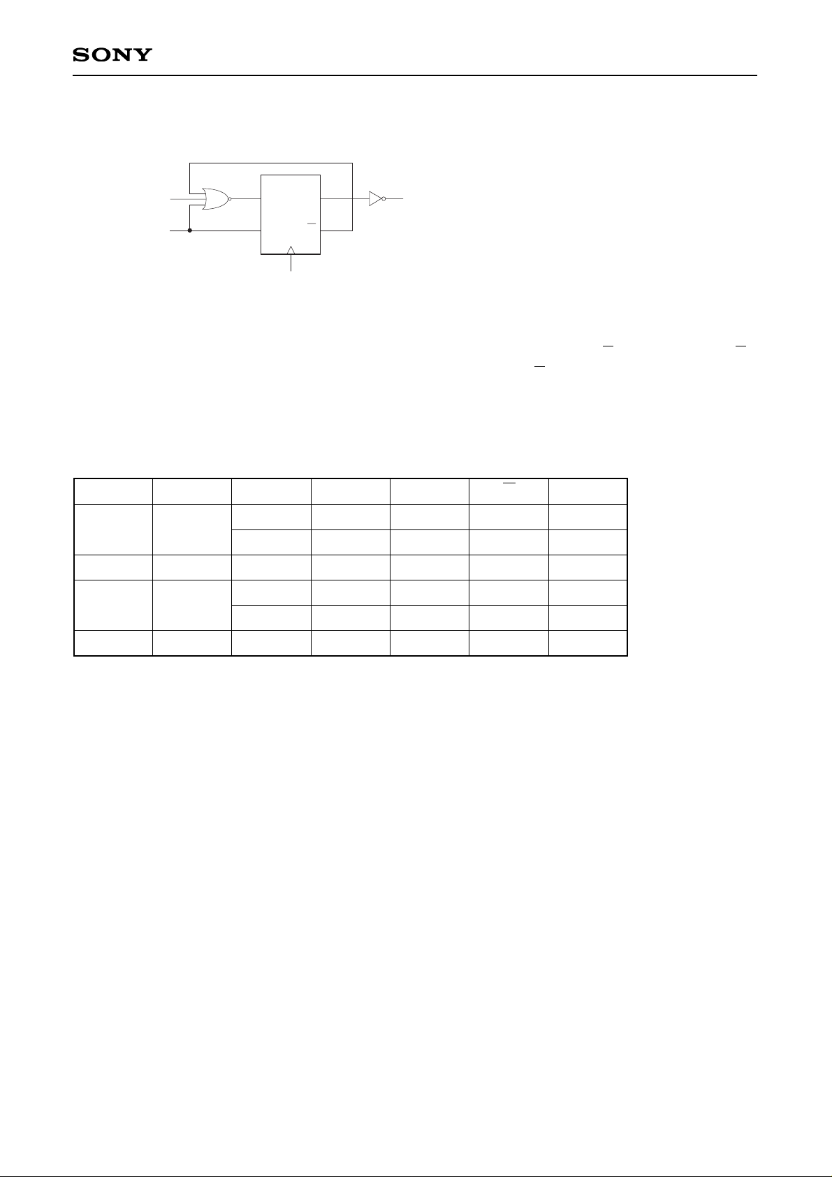
3. Relationship between SYNC input and DSYNC output during HOLD
J
K
Q
Q
CK
CLK
DSYNC
internal signal
SYNC
internal signal
DIVOUTN
internal signal
When the above SYNC internal and DIVOUTN internal signals are input, the DSYNC internal signal is output
as shown the table below.
First, when SYNC = L and DIVOUTN = L, it does not stand up because the output of Q = DSYNC = L and Q =
DSYNC = H∗∗(unchanged with the previous data) is exclusive logic. And, Q = DSYNC = H∗∗is the impossible
output. Therefore, it is as follows.
1. DSYNC = L when SYNC = L and DIVOUTN = L.
2. DSYNC = H∗or L∗(unchanged with the previous data) when SYNC = H and DIVOUTN = L.
3. DSYNC = H when DIVOUTN = H (SYNC = H or L)
SYNC
L
H
L
L
L
L
L
L
H
L
L
H
L
H
L
L
H
L
∗∗
∗
∗
H
L
H
H
L
H
∗∗
∗
∗
H
L
H
H
L
H
∗∗
∗
∗
L
H
L
H
L
L
H
H
DIVOUTN J K Q Q DSYNC
(∗) and (∗∗) are unchanged with the previous data.
Page 26

– 26 –
CXA3106AQ
The polarity of SYNC internal signal and DSYNC internal signal has a relationship between the setting of the
respective SYNC POL and DSYNC POL. The below diagrams are the examples that show the relationship
between SYNC input and DSYNC output and between the SYNC POL and DSYNC POL during HOLD.
CASE1
1/fSYNC 1/fSYNC 1/fSYNC 1/fSYNC 1/fSYNC 1/fSYNC 1/fSYNC
ThsThhThsThh
8CLK 8CLK 8CLK 8CLK 8CLK 8CLK
8CLK 8CLK
HOLD input
SYNC Input
SYNC internal signal
(SYNC POL = 1)
DIVOUTN
internal signal
DSYNC
internal signal
DSYNC output
(DSYNC POL = 1)
1/fSYNC 1/fSYNC 1/fSYNC 1/fSYNC 1/fSYNC 1/fSYNC 1/fSYNC
ThsThhThsThh
8CLK 8CLK 8CLK 8CLK 8CLK 8CLK
HOLD input
SYNC Input
SYNC internal signal
(SYNC POL = 0)
DIVOUTN
internal signal
DSYNC
internal signal
DSYNC output
(DSYNC POL = 0)
CASE2
Page 27

– 27 –
CXA3106AQ
1/fSYNC 1/fSYNC 1/fSYNC 1/fSYNC 1/fSYNC 1/fSYNC 1/fSYNC
Ths
ThhThs
Thh
8CLK 8CLK 8CLK
8CLK 8CLK 8CLK
HOLD input
SYNC Input
SYNC internal signal
(SYNC POL = 1)
DIVOUTN
internal signal
DSYNC
internal signal
DSYNC output
(DSYNC POL = 1)
CASE3
1/fSYNC 1/fSYNC 1/fSYNC 1/fSYNC 1/fSYNC 1/fSYNC 1/fSYNC
Ths
ThhThsThh
8CLK 8CLK 8CLK 8CLK 8CLK 8CLK
HOLD input
SYNC Input
SYNC internal signal
(SYNC POL = 0)
DIVOUTN
internal signal
DSYNC
internal signal
DSYNC output
(DSYNC POL = 0)
CASE4
Page 28

– 28 –
CXA3106AQ
1/fSYNC 1/fSYNC 1/fSYNC 1/fSYNC 1/fSYNC 1/fSYNC 1/fSYNC
ThsThhThsThh
8CLK 8CLK 8CLK 8CLK 8CLK 8CLK
HOLD input
SYNC Input
SYNC internal signal
(SYNC POL = 1)
DIVOUTN
internal signal
DSYNC
internal signal
DSYNC output
(DSYNC POL = 1)
CASE5
1/fSYNC 1/fSYNC 1/fSYNC 1/fSYNC 1/fSYNC 1/fSYNC 1/fSYNC
ThsThhThsThh
8CLK 8CLK 8CLK 8CLK 8CLK 8CLK
HOLD input
SYNC Input
SYNC internal signal
(SYNC POL = 0)
DIVOUTN
internal signal
DSYNC
internal signal
DSYNC output
(DSYNC POL = 0)
CASE6
Page 29

– 29 –
CXA3106AQ
4. UNLOCK timing
unlock
detect
UNLOCK
V
CC
Signal from phase
comparator
C
R1
R2
S2
I2
I1
S1
Outside the ICInside the IC
The unlock detect output is an open collector. When unlock detect output S1 goes high, the current I1 is pulled in.
The UNLOCK sensitivity can be adjusted by connecting external resistors (R1, R2) and a capacitor (C) to this output
pin as appropriate and changing these values. Operation during three modes is described below.
CASE 1: When there is no phase difference, that is to say, when the PLL is locked.
The S1 signal is low and the S2 signal is high.
The UNLOCK output remains low.
S1
S2
UNLOCK
threshold
level
CASE 2: When there is a phase difference, that is to say, when the S1 signal goes high and low as shown in
the figure below, the fall slew rate of the S2 signal is determined by the current I1 flowing into that
open collector. Therefore, increasing the resistance R1 causes the S2 signal fall slew rate to
become slower. Also, since the S2 signal rise slew rate is determined by the current I2, reducing
the resistance R2 causes the S2 signal rise slew rate to become faster. If this integrated S2 signal
does not fall below the threshold level of the next inverter, the UNLOCK signal stays low, and the
PLL is said to be locked.
S1
S2
UNLOCK
threshold
level
CASE 3: However, even if a phase difference exists as shown above, if the resistance R1 is reduced, the
current I1 flowing into the open collector increases, and the S2 signal fall slew rate becomes faster.
Also, if the resistance R2 is increased, the S2 signal rise slew rate becomes slower. If this
integrated S2 signal falls below the threshold level of the next inverter, the UNLOCK signal goes
from low to high, and the PLL is said to be unlocked.
S1
S2
UNLOCK
threshold
level
Page 30
– 30 –
CXA3106AQ
Charge Pump and Loop Filter Settings
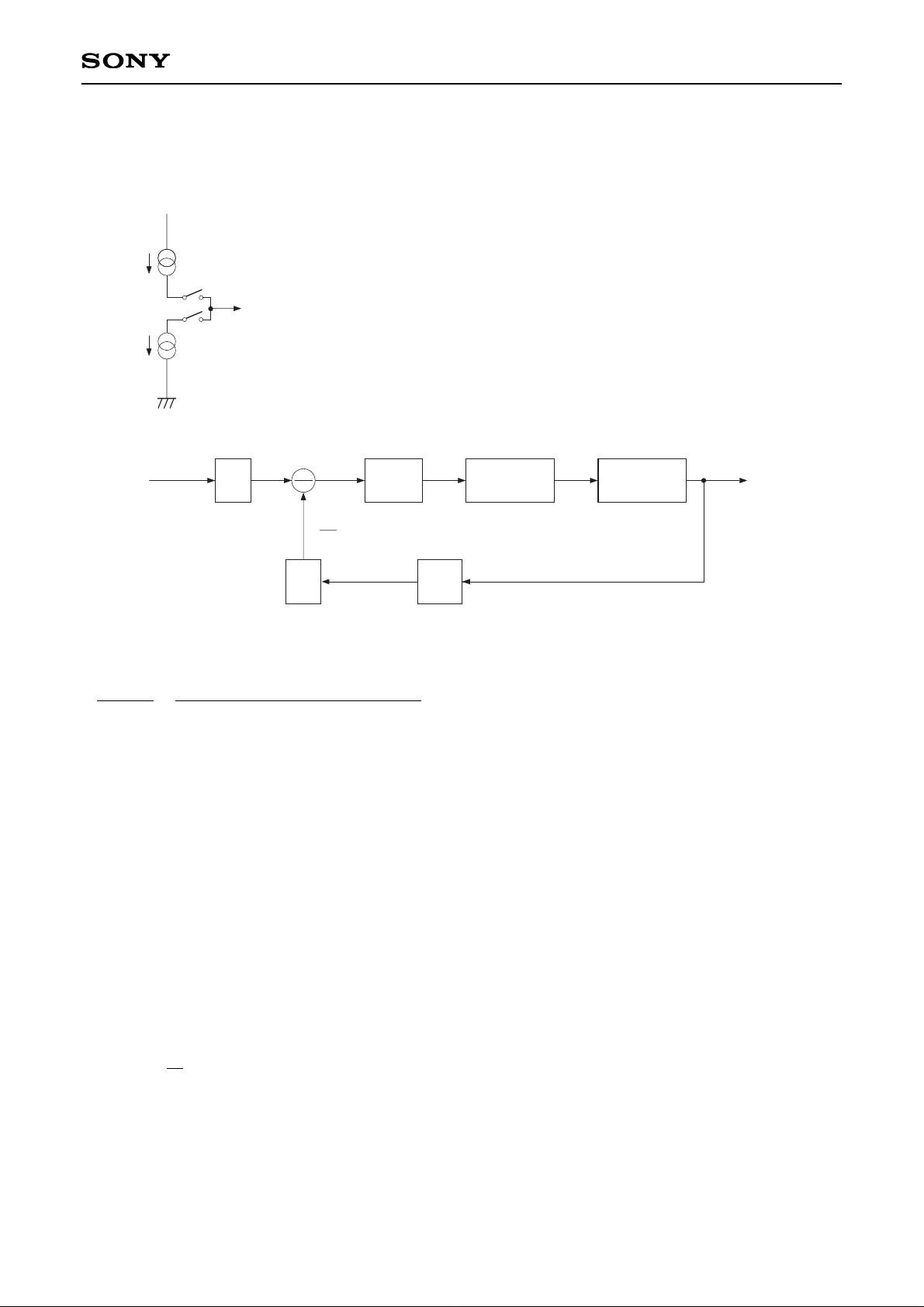
The CXA3106Q's charge pump is a constant-current output type as shown below.
S1
S2
To LPF
V
CC
When a constant-current output charge pump circuit is used inside the
PLL, the phase detector output acts as a current source, and the
dimension of its transmittance KPD is A/rad. Also, when considering the
VCO input as a voltage, the LPF transmittance dimension must be
expressed in ohms (Ω = V/A).
Therefore, the PLL transmittance when a constant-current output charge
pump circuit is used is as follows.
1/S
KPD
(A/rad)
F (S)
(Ω)
KVCO
(rad/sV)
1/S 1/N
PD
LPF VCO
counter
θo
N
ω
0
ω0/N
θr
ω
r
+
–
The PLL closed loop transmittance is obtained by the following formula.
Here, KPD, F (S), and KVCO are:
KPD: Phase comparator gain (A/rad)
F (S): Loop filter transmittance (Ω)
KVCO: VCO gain (rad/sV)
∗1
The reason for the 1/S inside the phase detector is as follows.
θo (t)/N =
∫
t
o ω0 (t)/Ndt + θo (t = 0)/N ... (a)
θo (t = 0) = 0
θo (t)/N =
∫
t
o ω0 (t)/Ndt ... (b)
Performing Laplace conversion:
θo (S)/N = W0 (S)/N ... (c)
1
S
θo/N
θr
KPD · F (S) · KVCO · 1/N · 1/S
1 + KPD · F (S) · KVCO · 1/N · 1/S
=
... (1)
Page 31

– 31 –
CXA3106AQ
The loop filter F (S) is described below.
The loop filter smoothes the output pulse from the phase comparator and inputs it as the DC component to the
VCO. In addition to this, however, the loop filter also plays an important element in determining the PLL
response characteristics.
Typical examples of loop filters include lag filters, lag-lead filters, active filters, etc. However, the
CXA3106AQ's LPF is a current input type active filter as shown below, so the following calculations show an
actual example of deriving the PLL closed loop transmittance when using this type of filter and then using this
transmittance to create a formula for setting the filter constants.
Current input type active filter
Vo
C R
i
i
–Vo
–1
–A
The filter transmittance is as follows.
+ VO = (R + )
F (S) = ·
= ·
∴τ = RC
Here, assuming A > 1, then:
F (S) =
...........................
(2)
Next, substituting (2) into (1) and obtaining the overall closed loop transmittance for the PLL:
=
...
(3)
=
............................................
(4)
ωn =
√
......................................................
(5)
ζ = ωnτ
.................................................................
(6)
The Bode diagram for formula (2) is as follows.
log w
log w
–45deg
0
–90
phase [deg]
log scale
gain [dB]
1
τ
2ζωnS + ωn
2
S2+ 2ζωnS + ωn
2
1 + SRC
SC
A
1 + A
1 + Sτ
SC
θo/N
θr
· S +
1 + Sτ
SC
A
1 + A
KPD · KVCO · τ
NC
KPD · KVCO
NC
· S +S2+
KPD · KVCO · τ
NC
KPD · KVCO
NC
KPD · KVCO
NC
VO
A
1
SC
1
2
Page 32

– 32 –
CXA3106AQ
Here, ωn and ζ are as follows.
ωn characteristic angular frequency:
The oscillatory angular frequency when PLL oscillation is assumed to have been maintained by the loop filter
and individual loop gains is called the characteristic angular frequency: ωn.
ζ damping factor:
This is the PLL transient response characteristic, and serves as a measure of the PLL stability. It is
determined by the loop gain and the loop filter.
A capacitor C2 is added to the actual loop filter.
This added capacitor C2 is used to reduce the R noise, and a value of about 1/10 to 1/1000 of C1 should be
selected as necessary.
Current input type active filter with added capacitor C2
Vo
C2
C1 R
i
i
–Vo
–1
–A
The filter transmittance is as follows.
F (S) =
=
..................
(7)
τ1 = C1 · R
τ2 =
Here, assuming C2 = C1/100, then:
τ2 =
= C1 · R
= τ1
The Bode diagram for formula (7) is as follows.
1
τ1
log w
log w
–45deg
0
–90
phase [deg]
log scale
gain [dB]
1
τ2
1 + C1 · R · S
S ((C1 + C2) + C1 · C2 · R · S)
1 + τ1 · S
S (C1 + C2) (1 + τ2 · S)
C1 · C2 · R
C1 + C2
C1 · C1/100 · R
C1 + C1/100
1
101
1
101
Page 33

– 33 –
CXA3106AQ
Next, the various parameters inside an actual CXA3106AQ are obtained.
The CXA3106AQ's charge pump output block and the LPF circuit are as follows.
S1
S2
To VCO
V
CC
C2
C1R1
100k
CXA3106Q
10020k
100µA
or 400µA
or 1600µA
100µA
or 400µA
or 1600µA
45
46
First, KPD is as follows.
KPD = 100µ/2π or 400µ/2π or 1600µ/2 π (A/rad)
Typical KVCO characteristics curves for the CXA3106Q's internal VCO are as follows.
2 3 4
50
100
150
VCO input voltage [V]
VCO frequency [MHz]
VCO DIV = 1/1
VCO DIV = 1/2
VCO DIV = 1/4
Therefore, KVCO is as follows.
KVCO = 2π · 65M or 2π · 32.5M or 2π · 16.25M (rad/sV)
Page 34

– 34 –
CXA3106AQ
ωn and ζ calculated for various types of computer signals are shown below.
Here, the various parameters are as follows.
FSYNC: Input H sync frequency
FCLK: Output clock frequency
KPD∗2π: Phase comparator gain ∗2π (KPD*2π = +100 or 400 or 1600)
KVCO/2π: VCO gain (when VCO DIV = 1/1, KVCO/2π = 65)
(when VCO DIV = 1/2, KVCO/2π = 65/2)
(when VCO DIV = 1/4, KVCO/2π = 65/4)
N: Counter value
C1: Loop filter capacitance value
R1: Loop filter resistance value
NTSC
NTSC
NTSC
PAL
PAL
PAL
PC-98
VGA
MAC
VESA
SVGA
SVGA
SVGA
SVGA
SVGA
MAC
XGA
XGA
XGA
MAC
XGA
SXGA
SXGA
SXGA
SXGA
Resolution
640 × 400
640 × 480
640 × 480
640 × 480
800 × 600
800 × 600
800 × 600
800 × 600
800 × 600
832 × 624
1024 × 768
1024 × 768
1024 × 768
1024 × 768
1024 × 768
1280 × 1024
1280 × 1024
1280 × 1024
1280 × 1024
FSYNC
kHz
15.734
15.734
15.734
15.625
15.625
15.625
24.82
31.47
35.00
37.86
35.16
37.88
46.88
48.08
53.67
49.72
48.36
56.48
60.02
60.24
68.68
46.43
63.98
79.98
91.15
FCLK
MHz
12.27
18.41
24.55
14.69
22.03
29.38
21.05
25.18
30.24
31.50
36.00
40.00
49.50
50.00
56.25
57.28
65.00
75.00
78.75
80.00
94.50
78.75
108.00
135.00
156.96
KPD
× 2π
µA
100
400
400
100
400
400
400
400
400
400
400
400
400
400
400
400
400
400
400
400
400
400
400
400
400
N
setting
780
1170
1560
940
1410
1880
848
800
864
832
1024
1056
1056
1040
1048
1152
1344
1328
1312
1328
1376
1696
1688
1688
1722
C1
µF
0.33
0.33
0.33
0.33
0.33
0.33
0.33
0.33
0.33
0.33
0.33
0.33
0.33
0.33
0.33
0.33
0.33
0.33
0.33
0.33
0.33
0.33
0.33
0.33
0.33
R1
Ω
3300
3300
3300
3300
3300
3300
3300
3300
3300
3300
3300
3300
3300
3300
3300
3300
3300
3300
3300
3300
3300
3300
3300
3300
3300
fn
kHz
0.40
0.65
0.57
0.36
0.59
0.52
0.77
0.79
0.76
0.77
0.99
0.97
0.97
0.98
0.98
0.93
0.86
0.87
0.87
0.87
1.20
1.08
1.09
1.09
1.08
ζ
1.37
2.23
1.93
1.25
2.04
1.76
2.62
2.70
2.60
2.65
3.38
3.33
3.33
3.35
3.34
3.18
2.95
2.97
2.98
2.97
4.12
3.71
3.72
3.72
3.68
C.Pump
setting
Bit1
0
1
1
0
1
1
1
1
1
1
1
1
1
1
1
1
1
1
1
1
1
1
1
1
1
KVCO/2π
MHz/V
65/4
65/4
65/4
65/4
65/4
65/4
65/4
65/4
65/4
65/4
65/2
65/2
65/2
65/2
65/2
65/2
65/2
65/2
65/2
65/2
65/1
65/1
65/1
65/1
65/1
Bit0
0
0
0
0
0
0
0
0
0
0
0
0
0
0
0
0
0
0
0
0
0
0
0
0
0
DIV1.2.4
setting
Bit1
1
1
1
1
1
1
1
1
1
1
1
1
1
1
1
1
1
1
1
1
0
0
0
0
0
Bit0
1
1
1
1
1
1
1
1
1
1
0
0
0
0
0
0
0
0
0
0
0
0
0
0
0
ωn
kHzrad
2.51
4.10
3.55
2.29
3.74
3.24
4.82
4.96
4.77
4.87
6.20
6.11
6.11
6.15
6.13
5.85
5.41
5.45
5.48
5.45
7.57
6.82
6.83
6.83
6.76
Page 35

– 35 –
CXA3106AQ
CLK Jitter Evaluation Method
The regenerated CLK is obtained by applying Hsync to the CXA3106AQ. Apply this CLK to a digital
oscilloscope and observe the CLK waveform using Hsync as the trigger.
Digital
Oscilloscope
CXA3106AQ
trigger
Pulse
Generator
ch1
CLKHsync
H
Sync
Back
Porch
Front
Porch
Active
Video
15 to 25% of Tsync
Tsync = 1/fsync
EnlargedEnlarged Enlarged Enlarged
CLK
Tjp-p
Trigger
CLK
Hsync
Computer signal
The CLK jitter is measured at peak to peak in the long-term write mode of the digital oscilloscope as shown in
the figure. The CLK jitter size varies according to the difference in the relative position with respect to Hsync.
Therefore, when the observation point is changed, the CLK jitter at that point is observed.
The figure below shows an typical example of the CLK jitter for the CXA3106AQ.
The CLK jitter increases slightly at the rising edge of Hsync (in the case of positive polarity), and then settles
down thereafter. However, this is not a problem as the active pixels start after about 20% of the H cycle has
passed from the rising edge of Hsync.
0 1/4 · Tsync 2/4 · Tsync 3/4 · Tsync Tsync
Observation points
Jitter amount [Tjp-p]
Page 36

– 36 –
CXA3106AQ
Coarse Delay Td1 vs Coarse Delay Bit
Coarse Delay Bit
0 31 2
1
3
4
5
Coarse Delay Td1 [CLK]
2
Ta = –25°C
Ta = +25°C
Ta = +75°C
Fine Delay Td2 vs Fine Delay Bit
Fine Delay Bit
0 205 10 15
0
10
15
20
25
Fine Delay Td2 [1/16 CLK]
5
Ta = –25°C
Ta = +25°C
Ta = +75°C
Jitter peak-peak [ns]
0 20 40 100 120 140 16060 80
0.0
1.0
2.0
3.0
4.0
5.0
Output Frequency [MHz]
Jitter peak-peak vs Output Frequency
NTSC/PAL, DIV = 1/4, CP = 10
VGA, DIV = 1/4, CP = 10
SVGA, DIV = 1/2, CP = 10
XGA, DIV = 1/2, CP = 10
SXGA, DIV = 1/1, CP = 11
1.5 2.0 2.5 4.0 4.53.0 3.5
0
50
100
150
200
250
Output Frequency [MHz]
VCO Control Voltage [V]
KVCO characteristics
DIV = 1/1
1.5 2.0 2.5 4.0 4.53.0 3.5
0
50
100
150
200
300
Output Frequency [MHz]
VCO Control Voltage [V]
KVCO Temperature characteristics
250
Ta = +75°C
Ta = +25°C
Ta = –25°C
DIV = 1/2
DIV = 1/4
Example of Representative Characteristics
Page 37

– 37 –
CXA3106AQ
Notes on Operation
• Be sure not to separate the analog and digital power supplies, and the analog and digital GND.
• The ground pattern should be as wide as possible. Using a multi-layer substrate with a mat ground is
recommended.
• Ground the power supply pins of the IC with a 0.1µF or larger ceramic chip capacitor as close to each pin as
possible.
• Be sure to accurately match the I/O characteristic impedance in order to ensure sufficient performance during
high-speed operation.
• Design the set so that the loop filter (external) is located at the minimum distance. (See the CXA3106AQ
PWB.)
Page 38

– 38 –
CXA3106AQ
(1) Recommended PECL I/O circuit
The peripheral circuits mainly use PECL for digital input and output. Of course, PECL and TTL can also be
mixed. In this case, disable the TTL outputs with the control registers.
∗3
GND VCC (+5.0V)
Control
Register
HOLD
SYNCH, SYNCL: PECL level
complementary input
100pF
0.33µF
3.3kΩ
1200pF
Loop Filter
∗
4
1.6kΩ 100Ω
V
CC
UNLOCK output
∗
2
GND
100kΩ
10nF
PECL level output pins
330Ω
GND
IOV
CC
IOGND
VCOH
VCOL
VCO
HOLD
SYNCH
SYNCL
SYNC
SENABLE
SCLK
SDATA
PECLV
CC
VBB
DSYNCH
DSYNCL
CLKH
CLKL
CLK/2H
CLK/2L
PECLV
CC
IOGND
TTLV
CC
TTLGND
DSYNC
CLK
CLKN
CLK/2
CLK/2N
DGND
DV
CC
UNLOCK
DIVOUT
SEROUT
CS
TLOAD
IOGND
IOV
CC
PLLVCC
PLLGND
VCOV
CC
VCOGND
VCOHGND
IREF
RC2
RC1
IRGND
IRV
CC
40
39
38
37
41
42
43
44
45
46
47
48
13
14
15
16
17
18
19
20
21
22
23
24
36
35
34
31
32
33
25
26
2728
29
30
2
3
4
5
6
7
8
9
10
11
12
1
Notes)
∗
1
Unless otherwise specified, all capacitors are 0.1µF.
∗
2
Vary the external resistor and capacitor values of the
UNLOCK output as necessary.
∗
3
This external resistor (1.6kΩ) should be a metal film
resistor in consideration of temperature characteristics.
∗
4
The loop filter's capacitors and resistor should also be
temperature compensated.
Page 39

– 39 –
CXA3106AQ
(2) Recommended TTL I/O circuit
The peripheral circuits mainly use TTL for digital input and output. Of course, PECL and TTL can also be
mixed.
∗
3
GND VCC (+5.0V)
Control
Register
HOLD
SYNC: TTL level input
100pF
0.33µF
3.3kΩ
1200pF
Loop Filter
∗
4
1.6kΩ 100Ω
V
CC
UNLOCK output
∗
2
GND
100kΩ
10nF
TTL level output pins
IOV
CC
IOGND
VCOH
VCOL
VCO
HOLD
SYNCH
SYNCL
SYNC
SENABLE
SCLK
SDATA
PECLV
CC
VBB
DSYNCH
DSYNCL
CLKH
CLKL
CLK/2H
CLK/2L
PECLV
CC
IOGND
TTLV
CC
TTLGND
DSYNC
CLK
CLKN
CLK/2
CLK/2N
DGND
DV
CC
UNLOCK
DIVOUT
SEROUT
CS
TLOAD
IOGND
IOV
CC
PLLVCC
PLLGND
VCOV
CC
VCOGND
VCOHGND
IREF
RC2
RC1
IRGND
IRV
CC
40
39
38
37
41
42
43
44
45
46
47
48
13
14
15
16
17
18
19
20
21
22
23
24
36
35
34
31
32
33
25
26
2728
29
30
2
3
4
5
6
7
8
9
10
11
12
1
Notes)
∗
1
Unless otherwise specified, all capacitors are 0.1µF.
∗
2
Vary the external resistor and capacitor values of the
UNLOCK output as necessary.
∗
3
This external resistor (1.6kΩ) should be a metal film
resistor in consideration of temperature characteristics.
∗
4
The loop filter's capacitors and resistor should also be
temperature compensated.
Page 40

– 40 –
CXA3106AQ
Connecting the CXA3106AQ with Sony ADC (Demultiplex Mode)
When connecting the PLL output to A/D converters with built-in demultiplex function such as the
CXA3026AQ/CXA3026Q/CXA3086Q (Sony), a simple system can be configured by connecting the CLK
(PECL) and CLKN (PECL) outputs of the CXA3106AQ to the CLK (PECL) and CLKN (PECL) inputs of each
A/D converter, respectively, and the 1/2 CLK (PECL) and 1/2 CLKN (PECL) outputs of the CXA3106AQ to
the RESETN (PECL) and RESET (PECL) inputs of each A/D converter, respectively. (when the PLL counter
value N is an even number)
Wiring Diagram
8 or 6
TTL
8 or 6
TTL
VIN
CLK (PECL)
CLKN (PECL)
RESETN (PECL)
RESET (PECL)
ADC
CXA3026AQ
CXA3026Q
CXA3086Q
8 or 6
TTL
8 or 6
TTL
VIN
CLK (PECL)
CLKN (PECL)
RESETN (PECL)
RESET (PECL)
ADC
CXA3026AQ
CXA3026Q
CXA3086Q
8 or 6
TTL
8 or 6
TTL
VIN
CLK (PECL)
CLKN (PECL)
RESETN (PECL)
RESET (PECL)
ADC
CXA3026AQ
CXA3026Q
CXA3086Q
CMOS LOGIC
CLK (TTL)
RESET (TTL)
DSYNC (TTL)
1/2 CLKN (PECL)
1/2 CLK (PECL)
CLKN (PECL)
CLK (PECL)
PLL
CXA3106AQ
• CXA3026AQ 8bit 140MSPS ADC
• CXA3026Q 8bit 120MSPS ADC
• CXA3086Q 6bit 140MSPS ADC
R
G
B
1/2 CLK
(TTL)
Page 41
– 41 –
CXA3106AQ
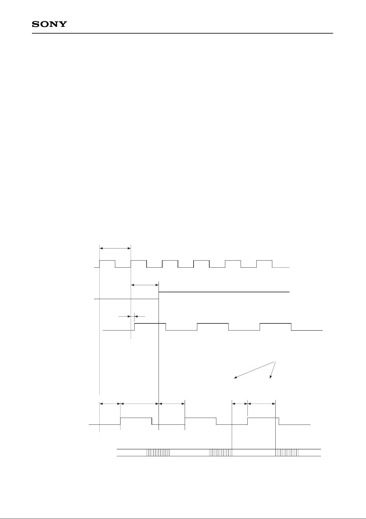
CXA3106AQ and Sony ADC (Demultiplex Mode) Timing
The CXA3106AQ and CXA3026Q/CXA3026AQ/CXA3086Q timings are shown below.
Here, the important timings are as follows.
(The clock cycle is labeled as T.)
• Within the A/D converters
Clock input vs. reset input
The setup time is T–1ns and the hold time is 0ns, satisfying the A/D converter specifications.
• Within the CMOS LOGIC at the rear end of the A/D converters
A/D converter data output vs. 1/2 clock output timing
The setup time is T–4.5ns and the hold time is T–0.5ns. (These timings also include combinations of
three A/D converters from different lots, and are defined for all operating temperatures and all operating
supply voltages. See the CXA3026Q/CXA3026AQ/CXA3086Q specifications for a detailed description.)
• Within the CMOS LOGIC at the rear end of the A/D converters
DSYNC signal from CXA3106AQ vs. A/D converter 1/2 clock output
The setup time is T–3ns and the hold time is T–5ns.
CLK (PECL)
out
T
3 to 7.5ns
0 to 1ns
4.5 to 8ns
Thold min.
T–5ns
Tsetup min.
T–3ns
Tsetup min.
T–4.5ns
Thold min.
T–0.5ns
DSYNC (TTL)
out
1/2CLK (PECL)
out
1/2CLK (TTL)
out
DATA (TTL)
out
CXA3026Q
CXA3026AQ
CXA3086Q
CXA3106AQ
∗
See the CXA3026AQ/Q and
CXA3086Q specifications.
Page 42

– 42 –
CXA3106AQ
Connecting the CXA3106AQ with Sony ADC (Straight Mode)
When connecting the PLL output to A/D converters such as the CXA3026AQ/CXA3026Q/CXA3086Q (Sony),
a simple system can be configured as shown below.
Wiring Diagram
8 or 6
TTL
VIN
CLK (PECL)
CLKN (PECL)
ADC
CXA3026AQ
CXA3026Q
CXA3086Q
8 or 6
TTL
VIN
CLK (PECL)
CLKN (PECL)
ADC
CXA3026AQ
CXA3026Q
CXA3086Q
8 or 6
TTL
VIN
CLK (PECL)
CLKN (PECL)
ADC
CXA3026AQ
CXA3026Q
CXA3086Q
CMOS LOGIC
CLK (TTL)
RESET (TTL)
DSYNC (TTL)
CLK (TTL)
CLKN (PECL)
CLK (PECL)
PLL
CXA3106AQ
• CXA3026AQ 8bit 140MSPS ADC
• CXA3026Q 8bit 120MSPS ADC
• CXA3086Q 6bit 140MSPS ADC
R
G
B
Page 43

– 43 –
CXA3106AQ
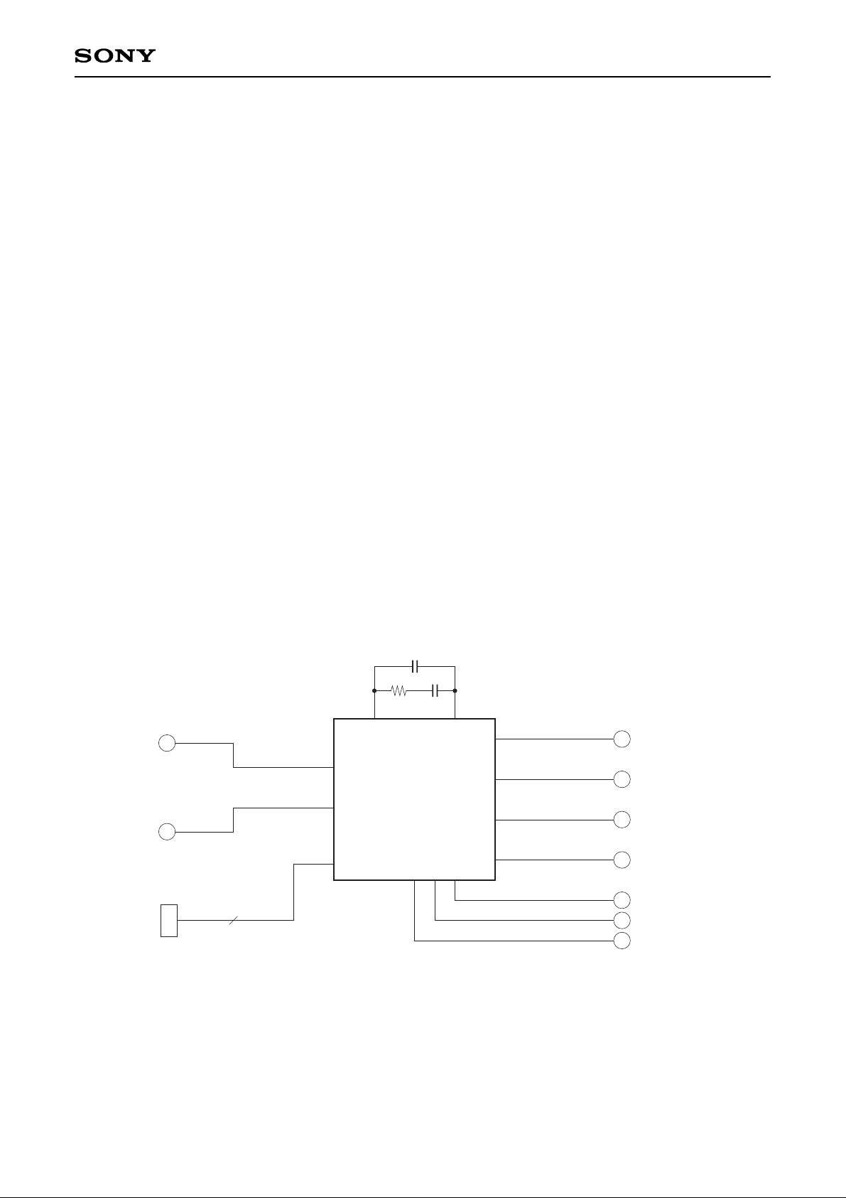
CXA3106AQ and Sony ADC (Straight Mode) Timing
The CXA3106AQ and CXA3026Q/CXA3026AQ/CXA3086Q timings are shown below.
Here, the important timings are as follows.
(The clock cycle is labeled as T.)
• Within the CMOS LOGIC at the rear end of the A/D converters
A/D converter data output vs. clock output from CXA3106AQ
The setup time is T–8.5ns and the hold time is 2ns. (These timings also include combinations of three A/D
converters from different lots, and are defined for all operating temperatures and all operating supply
voltages. See the CXA3026Q/CXA3026AQ/CXA3086Q specifications for a detailed description.)
• Within the CMOS LOGIC at the rear end of the A/D converters
DSYNC signal from CXA3106AQ vs. clock output from CXA3106AQ
The setup time is T–4.5ns and the hold time is 1.5ns.
CLK (PECL)
out
T
1.5 to 4.5ns
1.5 to 3ns
6.5ns min
Thold min.
2ns
CLK (TTL)
out
DSYNC (TTL)
out
DATA (TTL)
out
CXA3026Q
CXA3026AQ
CXA3086Q
CXA3106AQ
Tsetup min.
T–8.5ns
Tsetup min.
T–4.5ns
Thold min.
1.5ns
10ns max
Page 44
– 44 –
CXA3106AQ
CXA3106AQ-PWB (CXA3106AQ Evaluation Board)
The CXA3106AQ-PWB is an evaluation board for the CXA3106AQ PLL-IC. This board makes it possible to
easily evaluate the CXA3106AQ's performance using the supplied control program (Note: IBM PC/AT, MSDOS 5.0 and newer US mode specifications).
Features
• Two input level (TTL and PECL) SYNC input
• Two output level (TTL and PECL) CLK, CLK2 and DSYNC output
• Supply voltage: +5.0V
Absolute Maximum Ratings (Ta = 25°C)
Supply voltage VCC –0.5 to +7.0 V
Recommended Operating Conditions
• Supply voltage VCC 4.75 to 5.25 V
GND 0 V
• Digital input (PECL) DIN (High) VCC – 1.1 V (Min.)
DIN (Low) VCC – 1.5 V (Max.)
(TTL) DIN (High) GND + 2.0 V (Min.)
DIN (Low) GND + 0.8 V (Max.)
• Operating ambient temperature
Ta –20 to +75 °C
Block Diagram
VCO input
(PECL/TTL)
CXA3106AQ
48pin QFP
3
Loop Filter
SYNC input
(PECL/TTL)
CONTROL BUS (TTL)
SENABLE, SCLK, SDATA
DSYNC output
(PECL/TTL)
CLK output
(PECL/TTL)
CLK/2 output
(PECL/TTL)
VBB (PECL)
SEROUT (TTL)
DIVOUT (TTL)
UNLOCK (TTL)
Page 45

– 45 –
CXA3106AQ
Setting Methods and Notes on Operation
Input pins
This PWB supports TTL single and PECL complementary input.
Input pins: SYNC: TTL level input, 10 to 100kHz
SYNCL: PECL low level input, 10 to 100kHz
SYNCH: PECL high level input, 10 to 100kHz
VCO: TTL level input. This is a test pin and is therefore normally not used.
VCOL: PECL low level input. This is a test pin and is therefore normally not used.
VCOH: PECL high level input. This is a test pin and is therefore normally not used.
Output pins
This PWB supports TTL single and PECL complementary output.
DSYNCH,
DSYNCL: PECL level complementary delay SYNC outputs. The output range is 10 to 160kHz.
DSYNC: TTL level delay SYNC output. The output range is 10 to 100kHz.
CLKH,
CLKL: PECL level complementary CLK outputs. The output range is 10 to 160MHz.
CLK,
CLKN: TTL level complementary CLK outputs. The output range is 10 to 80MHz.
CLK/2H,
CLK/2L: PECL level complementary 1/2 CLK outputs. The output range is 5 to 80MHz.
CLK/2,
CLK/2N: TTL level complementary CLK outputs. The output range is 5 to 80MHz.
VBB: Outputs the PECL amplitude threshold voltage.
SEROUT: TTL level control register serial data output.
DIVOUT: TTL level internal programmable counter test output.
UNLOCK: TTL level UNLOCK output. This pin requires external circuits such as appropriate capacitors and
resistors.
See the IC specifications for a detailed description.
PECL outputs (VBB, DSYNCH, DSYNCL, CLKH, CLKL, CLK/2H, CLK/2L) are output constantly, but TTL
outputs (DSYNC, CLK, CLKN, CLK/2, CLK/2N, SEROUT, DIVOUT, UNLOCK) are controlled by the respective
control registers. Therefore, the enable/disable settings should be made in accordance with the application.
See the following pages for the setting method.
Page 46
– 46 –
CXA3106AQ
Jumper Wire Settings
S1, S2: These enable/disable HOLD (Pin 6). HOLD is active high, so the jumper wire should be connected to
S2 (HOLD = low) for normal use. When using HOLD, connect the jumper wire to S1 (HOLD = high).
(For the initial setting, the jumper wire is connected to S2.)
S3, S4: These enable/disable TLOAD (Pin 13). Connect the jumper wire to S4 (TLOAD = high) for normal use.
When using TLOAD, connect the jumper wire to S3 (TLOAD = low). (For the initial setting, the jumper
wire is connected to S4.)
S5, S6: These enable/disable CS (Pin 14). Connect the jumper wire to S6 (CS = high) for normal use. When
using Power Save, connect the jumper wire to S5 (CS = low). (For the initial setting, the jumper wire is
connected to S6.)
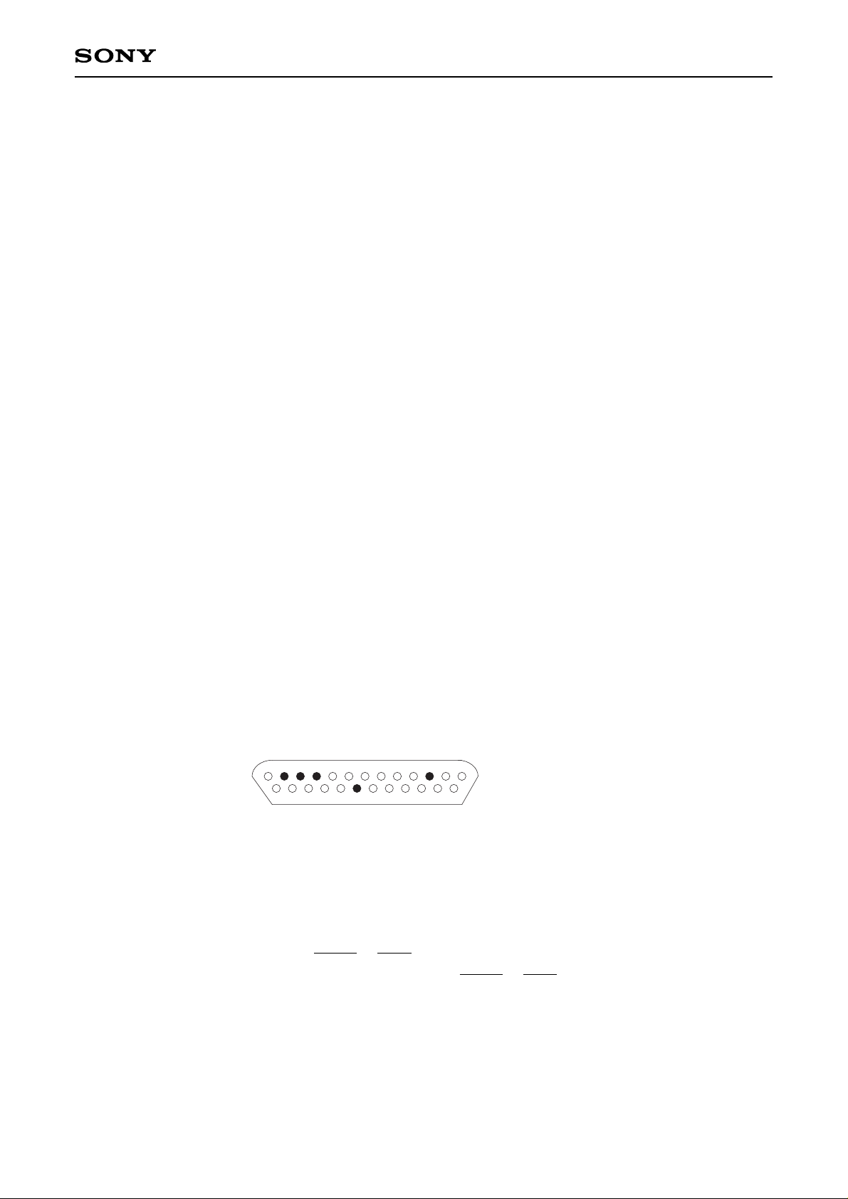
Supplied Program
This PWB is equipped with a control program that facilitates evaluation of the CXA3106AQ. Operation
methods and precautions are as follows.
1) Compatible personal computers
Use an IBM PC/AT or compatible machine equipped with a 25-pin D-SUB parallel port (printer port). Also,
operating systems which support the program are MS-DOS 5.0 or newer and MS-Windows 3.1 or newer.
(When using Windows, start the program from the DOS window.)
2) Connect the supplied cable
Connect the supplied cable to the parallel port of the personal computer and the DBUS1 connector of the
CXA3106AQ-PWB.
1 13
14 25
D-SUB 25-pin parallel connector pin arrangement
2pin : SCLK
3pin : SDATA
4pin : SENABLE
11pin : SERIN
19pin : GND
3) Connect the power cable and supply power to the CXA3106AQ-PWB
4) Start the program
A) Boot the personal computer and then shift to the directory containing the program.
B) Set MS-DOS to US mode. → US Return or Enter
C) Input the program name. →∗1CXA3106A or CXA3106B Return or Enter → Move to the program screen.
∗1
Only one of either CXA3106A or CXA3106B can be used as the program name depending on the printer
port setting of the personal computer.
Page 47

– 47 –
CXA3106AQ
5) Description of the program screen
A) When the program is started, the following initial screen is displayed.
Please type the name of the initialization file OR press ENTER.
The file extention.INI should not be included. The default file
when ENTER is pressed is CXA3106.INI
Filename > _
When this screen appears, press the Return or Enter key. The screen shifts to the function setting screen.
B) Function settings
When the program is loaded, the following function setting screen appears.
CXA3106 PLL REGISTERS
Divisor 1344
Divider 2
Coarse Delay 00 Fine Delay 10
Charge Pump 10
Polarity Power
SYNC DSYNC PD SCAN SYNTH VCO Bypass
1 1 1 OFF ON ON
O/P Enable
DIVOUT UNLOCK DSYNC CLK2 NCLK2 CLK1 NCLK1
OFF OFF OFF OFF OFF OFF OFF
Use arrow keys to select data bit. Press ENTER to toggle and load data.
Use Pg Up and Pg Dn to increment/decrement divisor and fine delay registers.
Press a to abort, s to scan registers MIXED SIGNAL SYSTEMS JAN 1997
Page 48
– 48 –
CXA3106AQ
Divisor
This is used to input the frequency division ratio of the program counter. The value can be changed as
desired from 9 to 4111 by moving the cursor to the position of the number and pressing the Return or Enter
key. (Note: The operating range of the CXA3106AQ is from 256 to 4096.) The value can also be incremented
or decremented by one step by pressing the Page Up or Page Down key, respectively.
The internal VCO has an oscillator frequency of 40 to 160MHz, so the output frequency and Divider (VCO
frequency divider) setting range are as follows.
Divider = 4
50 100 150
1/4
1/2
1/1
O/P Frequency [MHz]
Divider
40 160Divider = 1
20 80Divider = 2
10 40
Divider
This sets the VCO output frequency division ratio to 1/1, 1/2 or 1/4. The frequency division ratio changes
repeatedly in the order of 1/1 → 1/2 → 1/4 → 1/1 each time the cursor is moved to the position of the number
and the Return or Enter key is pressed.
Coarse Delay
This is the DSYNC upper delay time setting. The value can be changed by moving the cursor to the position
of the number and pressing the Return or Enter key. The delay time variable range settings are "00" (1 CLK),
"01" (2 CLK), "10" (3 CLK) or "11" (4 CLK).
Fine Delay
This is the DSYNC lower delay time setting. The value can be changed by moving the cursor to the position
of the number and pressing the Return or Enter key. The value can also be incremented or decremented by
one step by pressing the Page Up or Page Down key, respectively. The delay time can be varied from 1/16
CLK to 32/16 CLK by setting "0" to "31", respectively.
Charge Pump
This is the charge pump circuit KI setting. The value can be changed by moving the cursor to the position of
the number and pressing the Return or Enter key. KI can be set to "00" (about 100µA), "10" (about 400µA) or
"11" (about 1.6mA).
The setting "01" is not used. (Setting "01" is the same as setting "00".)
Polarity
These are the SYNC, DSYNC and PD (Phase Detector) polarity inversion settings, and should be set as
necessary such as when inverting the SYNC input and DSYNC output waveforms. The setting value "1" is
positive polarity, and "0" is negative polarity. These should normally all be set to "1". (Fix PD to "1" other than
during test mode.)
Page 49

– 49 –
CXA3106AQ
Power
SCAN: This is the control register read setting. When this is ON, the control register serial data is
output from SEROUT (Pin 15). This should normally be set to OFF.
SYNTH: This is the enable/disable setting for this IC. This should normally be set to ON.
VCO Bypass: This is set to OFF when testing the program counter. This should normally be set to ON.
O/P Enable
These are the enable/disable settings for each TTL output (DIVOUT, UNLOCK, DSYNC, CLK2, NCLK2,
CLK1 and NCLK1). Set to ON when performing evaluation using TTL output.
Page 50

– 50 –
CXA3106AQ
SCAN RESULT, CXA3106 PLL REGISTERS
Register 1 DIVREG1 00111000
Register 2 DIVREG2 0101
Register 3 CENFREREG 1011111
Register 4 DELAYREG 0010000
Register 5 CPREG 100
Register 6 TTLPOLREG 00000011
Register 7 TESTPOWREG 0111
Press r to return to PLL REGISTERS MENU.
Press a to abort MIXED SIGNAL SYSTEMS AUG 1996
C) Description of readout mode
This program has a function (readout mode) that reads the contents written to the control registers from the
CXA3106AQ SEROUT (Pin 15) and displays these contents on the screen. This function is described below.
1) Set SCAN to ON at the function setting screen.
2) Press the S key.
The following screen appears.
This screen conforms to the Control Register Table listed in the CXA3106AQ specifications.
3) Press the R key to return to the original function setting screen.
D) Quit the program
Press the A key to quit the program.
Page 51

– 51 –
CXA3106AQ
Substrate Pattern (parts surface)
Substrate Pattern (solder surface)
Page 52

– 52 –
CXA3106AQ
Silk Screen (parts surface)
Silk Screen (solder surface)
C1
C14
C18
C17
C13
C15C16
C10
C9
C8
C12
C19
C20
C11
C7
C3
C2
C4
C6
C18
C5
VCO
BNC3
VCOL
BNC2
VCOH
BNC1
VCC
SYNCH
BNC4
SYNCL
BNC5
SYNC
BNC6
S1
S2
R19
IC1
S3
S4
S5
S6
PR2
SEROUT
PR3
DIVOUT
PR4
UNLOCK
PR11
CLK/2N
PR12
CLK/2
PR13
CLKN
PR14
CLK
PR15
DSYNC
PR1
CLK/2L
PR5
CLK/2H
R6
R13
R5
R12
PR6
CLKL
PR7
CLKH
R7
R14
R4
R11
PR8
DSYNCL
PR9
DSYNCH
R3
R10
R2
R9
PR10
VBB
R1
R8
C21
33µ
+
CXA3106Q/AQ PWD v1.2
DBUS1
Control Register
GND
Page 53

– 53 –
CXA3106AQ
PWB Circuit Diagram
S1
S2
C2
0.1µ
C3
0.1µ
C19
0.33µ
C20
1200p
R18
3.3k
GND
R19
1.6k
C11
100p
C4
0.1µ
C5
0.1µ
C6
0.1µ
C12
0.1µ
C7
0.1µ
S3 S4
S5
S6
C9
0.1µ
GND
GND
C8
0.1µ
C10
0.1µ
V
CC
R8 330R1
R9 330R2
R10 330
R3
R11 330
R4
R14 330
R7
R12 330
R5
R13 330
R6
VCC
PR10A
VBB
PR9A
DSYNCH
PR8A
DSYNCL
PR7A
CLKH
PR6A
CLKL
PR5A
CLK/2H
PR1A
CLK/2L
PR15A
DSYNC
PR14A
CLK
PR13A
CLKN
PR12A
CLK/2
PR11A
CLK/2N
C1
0.1µ
C13
0.1µ
C14
0.1µ
C15
0.1µ
C18
0.1µ
C16
0.1µ
C17
0.1µ
GND
VCC
C21
33µ
PWR1
V
CC
PWR2
GND
PR3A
DIVOUT
PR4A
UNLOCK
PR2A
SEROUT
1
5
DBUS1
Control Register
GND
BNC6
SYNC
BNC5
SYNCL
BNC4
SYNCH
BNC3
VCO
BNC2
VCOL
BNC1
VCOH
IOGND
IOV
CC
PLLV
CC
PLLGND
VCOV
CC
VCOGND
VCOHGND
IREF
RC2
RC1
IRGND
IRV
CC
40
39
38
37
4142
43
44
45
46
47
48
DSYNC
CLK
CLKN
CLK/2
CLK/2N
DGND
DV
CC
UNLOCK
DIVOUT
SEROUT
CS
TLOAD
13
14
15
16
17
18
19
20
21
22
23
24
PECLV
CC
VBB
DSYNCH
DSYNCL
CLKH
CLKL
CLK/2H
CLK/2L
PECLV
CC
IOGND
TTLV
CC
TTLGND
36
35
34
31
32
33
25
26
27
28
29
30
IOV
CC
IOGND
VCOH
VCOL
VCO
HOLD
SYNCH
SYNCL
SYNC
SENABLE
SCLK
SDATA
2
3
4
5
6
7
8
9
10
11
12
1
CXA3106AQ
Note) R1 to R7 are not mounted.
Page 54

– 54 –
CXA3106AQ
Package Outline Unit: mm
SONY CODE
EIAJ CODE
JEDEC CODE
M
PACKAGE STRUCTURE
PACKAGE MATERIAL
LEAD TREATMENT
LEAD MATERIAL
PACKAGE WEIGHT
EPOXY RESIN
SOLDER / PALLADIUM
PLATING
COPPER / 42 ALLOY
48PIN QFP (PLASTIC)
15.3 ± 0.4
12.0 – 0.1
+ 0.4
0.8 0.3 – 0.1
+ 0.15
± 0.12
13
24
2536
37
48
1 12
2.2 – 0.15
+ 0.35
0.9 ± 0.2
0.1 – 0.1
+ 0.2
13.5
0.15
0.15 – 0.05
+ 0.1
QFP-48P-L04
∗QFP048-P-1212-B
0.7g
NOTE : PALLADIUM PLATING
This product uses S-PdPPF (Sony Spec.-Palladium Pre-Plated Lead Frame).
Sony Corporation
 Loading...