

Page 1

RF Matrix Amplifier
Description
The CXA2570N is an IC developed for the RF signal
processing of compact disc players.
Features
• Wide band RF signal processing
• RF system VCA circuit
• RF system equalizer (supports CAV mode)
• Supports pickups with built-in RF summing amplifier
• Low power consumption mode (EQ Pass mode)
• RW/ROM switching mode
Functions
• RFAC summing amplifier, equalizer, VCA
• RFDC summing amplifier
• Focus error amplifier
• Tracking error amplifier
• Automatic power control
• VC buffer amplifier
Applications
CD-ROM/RW compatible systems
Structure
Bipolar silicon monolithic IC
Absolute Maximum ratings
• Supply voltage Vcc 7 V
• Operating temperature Topr –20 to +75 °C
• Storage temperature Tstg –65 to +150 °C
• Allowable power dissipation
PD 620 mW
Operating Conditions
• Supply voltage Vcc – GND 3.0 to 5.5 V
• Operating temperature Topr –20 to +75 °C
– 1 –
E98259A98-PS
Sony reserves the right to change products and specifications without prior notice. This information does not convey any license by
any implication or otherwise under any patents or other right. Application circuits shown, if any, are typical examples illustrating the
operation of the devices. Sony cannot assume responsibility for any problems arising out of the use of these circuits.
CXA2570N
24 pin SSOP (Plastic)
Page 2
– 2 –
CXA2570N
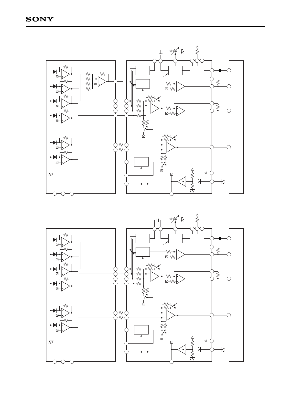
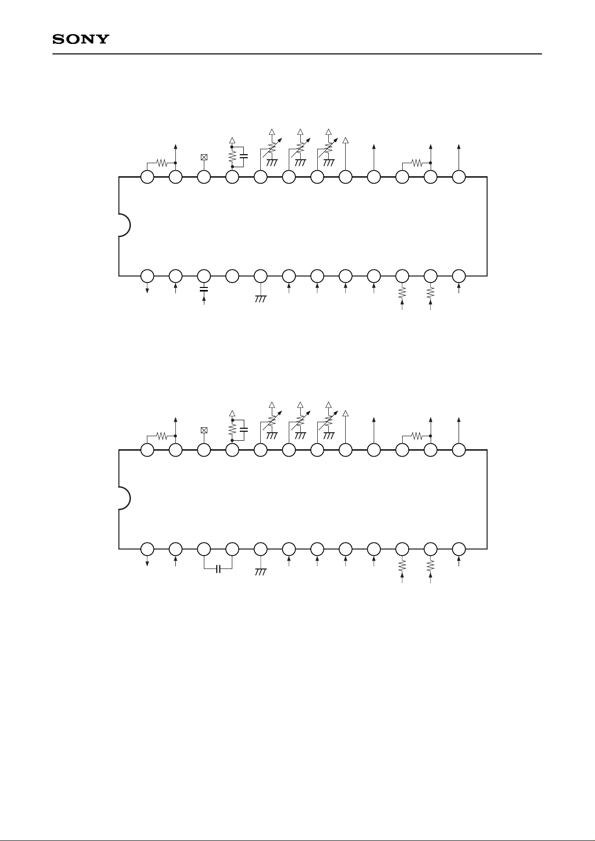
Connected Circuit Diagram
VC
RF
VC
A
A
B
C
D
A
B
C
D
A
B
C
D
AC
SUM
DC
SUM
VC
B
VC
VC
FE
FE
FEI
100k
VC
C
VC
D
VC
F F
E
F
E
VC
E
RFDCI
RFAC
RFAC
RFDCO
RFDC
5.1k
VC
ACG
RW/ROM RW/ROM
RW/ROM
RW/ROM
Rfc Vfc
5.1k
<DSP>
<OP (with RF_SUM)>
EQIACSUM BST
V
CC
VCC
VCC
TE
TE
GND
V
CC
0.1µ
AC
VCA
EQ
APC
VC
VC
RW/ROM
RW/ROM
PD
LD
SW
10k
10k
APC-OFF (Hi-Z)
RW/ROM
(H/L)
VCVCC GND
VCC
VCC
VCC
VC
A
A
B
C
D
A
B
C
D
AC
SUM
DC
SUM
VC
B
VC
VC
FE
FE
FEI
100k
VC
C
VC
D
VC
F F
E
F
E
VC
E
RFDCI
RFAC
RFAC
RFDCO
RFDC
5.1k
VC
ACG
RW/ROM RW/ROM
RW/ROM
RW/ROM
Rfc Vfc
5.1k
<DSP>
<OP (without RF_SUM)>
EQI
ACSUM
BST
V
CC
VCC
TE
TE
GND
0.1
AC
VCA
EQ
APC
VC
VC
RW/ROM
RW/ROM
PD
LD
SW
10k
10k
APC-OFF (Hi-Z)
RW/ROM
(H/L)
VC GNDVCC
VCC
Page 3
– 3 –
CXA2570N
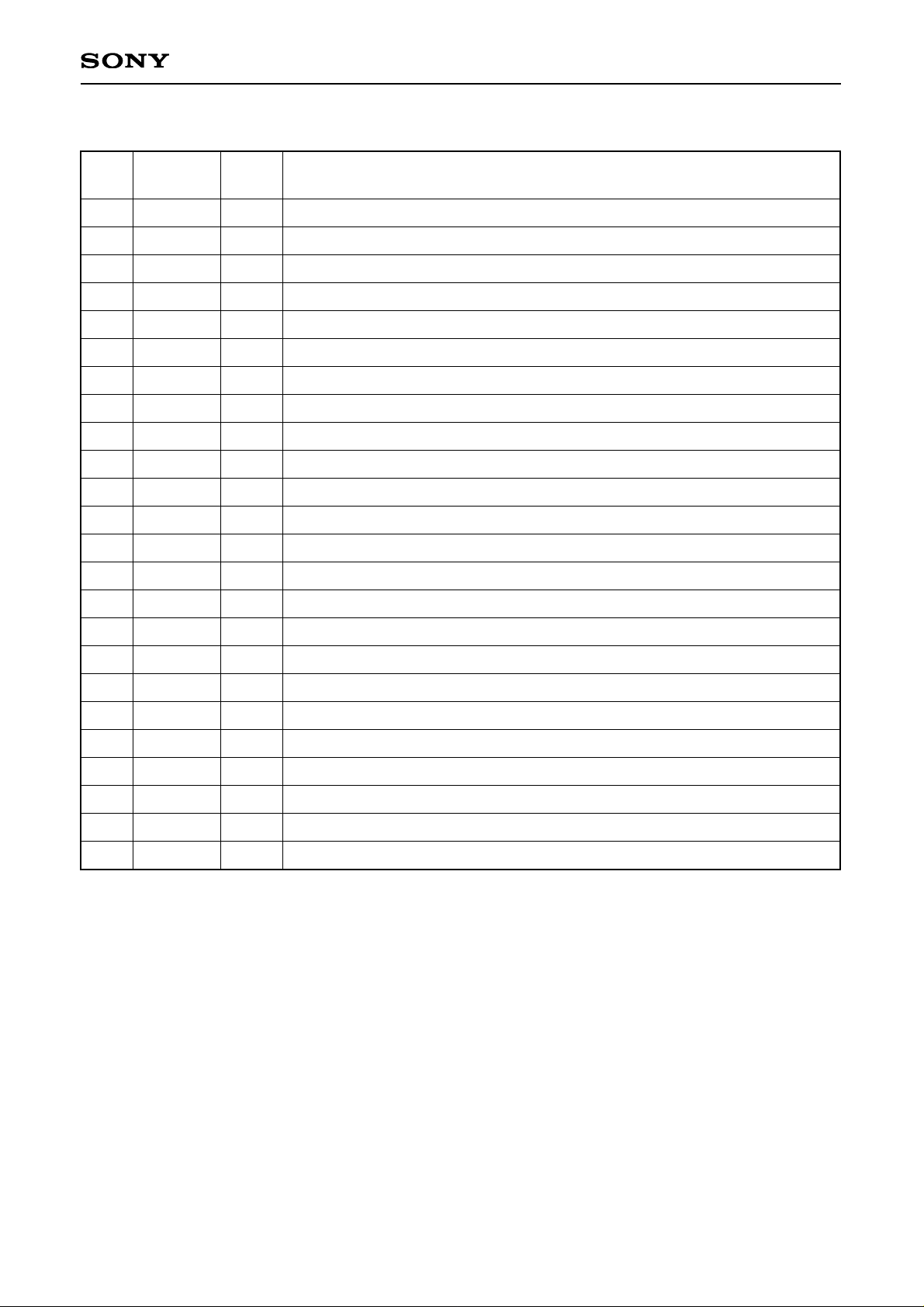
Pin Description
Pin
No.
1
2
3
4
5
6
7
8
9
10
11
12
13
14
15
16
17
18
19
20
21
22
23
24
LD
PD
EQ_IN
AC_SUM
GND
A
B
C
D
E
F
SW
RFAC
FE
FEI
TE
VCC
RFG
BST
VFC
RFC
VC
RFDCO
RFDCI
Out
In
In
Out
In
In
In
In
In
In
In
In
Out
Out
—
Out
In
In
In
In
In
Out
Out
—
APC amplifier output.
APC amplifier input.
RFAC system VCA block and EQ block input.
RFAC system RF SUM output.
Ground.
A signal input.
B signal input.
C signal input.
D signal input.
E signal input.
F signal input.
Mode switching signal input.
RFAC signal output.
Focus error signal output.
FE amplifier virtual ground.
Tracking error signal output.
VCC.
RFAC system VCA block low-frequency gain adjustment.
EQ boost amount adjustment range.
EQ cut-off frequency adjustment.
EQ cut-off frequency adjustment.
VC voltage output.
RFDC signal output.
RFDC amplifier virtual ground.
Symbol I/O Description
Page 4

– 4 –
CXA2570N
Pin Description and Equivalent Circuit
Pin
No.
1
2
3
4
5
O
I
I
O
— —
APC amplifier output.
APC amplifier input.
Equalizer circuit input.
RFAC summing amplifier
output.
Ground.
LD
PD
EQ_IN
AC_SUM
GND
Symbol I/O Equivalent circuit Description
10k
1k
1
20k
55k
20k
2
VCVC
1.2k
5k5k
1.1k1.1k
3
1.6k
1.6k
4
Page 5

– 5 –
CXA2570N
Pin
No.
6 I
RF summing amplifier and
focus error amplifier input.
A
7 IB
8 IC
9 ID
10 I
Tracking error amplifier input.
E
11 I
Tracking error amplifier output.
F
16 OTE
CD-ROM/RW switching input.
RW when connected to VCC,
ROM when connected to
GND.
12ISW
RFAC amplifier output.
13ORFAC
Symbol I/O Equivalent circuit Description
VC
47k
47k
15k
7
30k
100µA
100µA
100µA
100µA
6
8
9
27k 27k
124
10
11
16
200k
12
200k
200k
100
2mA
13
Focus error amplifier output.
Focus error amplifier gain
adjustment. The gain is
adjusted by the external
resistance value connected
between this pin and Pin 14.
14
15
O
FE
IFEI
VC
50k
124
15
124
14
Page 6

– 6 –
CXA2570N
Pin
No.
17 — —
Power supply.
VCC
Symbol I/O Equivalent circuit Description
18
I
Sets the RFAC low-frequency
gain.
RFG
100µA
VC
20k
18
19
I
Input for adjusting the
equalizer circuit boost amount.
BST
20k
50µA
VC
19
20
I
Input for adjusting the
equalizer circuit boost
frequency with the control
voltage.
VFC
100µA
VC
20k
20
21
I
Input for adjusting the
equalizer circuit boost
frequency with external
resistance.
RFC
124
1.0V
21
22
O
(VCC + GND)/2 voltage output.
VC
23
O
RFDC amplifier output. This
pin serves as the eye pattern
check point.
RFDC
24
I
RFDC amplifier gain
adjustment. The gain is
adjusted by the external
resistance value connected
between this pin and Pin 23.
RFDCI
25
150k
150k
22
124
VC
1mA
1.5k
124
23
24
Page 7

– 7 –
CXA2570N
Measure-
ment No.
1
2
3
4
5
6
7
8
9
10
11
12
13
14
15
16
17
18
19
20
21
22
23
24
25
26
27
28
29
30
Current consumption (Active, EQ On)
Current consumption (Active, EQ Off)
Current consumption (Sleep)
SUM offset voltage
SUM frequency gain
SUM frequency response
SUM maximum output voltage H
SUM maximum output voltage L
Offset voltage ROM
Offset voltage RW
Low-frequency gain ROM_min
Low-frequency gain ROM_cnt
Low-frequency gain ROM_max
Low-frequency gain RW_min
Low-frequency gain RW_cnt
Low-frequency gain RW_max
Low-frequency gain EQ_off
Frequency response Min_L
Frequency response Min_H
Frequency response EQ_OFF
Maximum output voltage H
Maximum output voltage L
Offset voltage ROM
Offset voltage RW
Low-frequency gain ROM
Low-frequency gain RW
Frequency response ROM
Frequency response RW
Maximum output voltage H
Maximum output voltage L
Icc_Aeqon
Icc_Aeqoff
Icc_Slp
ACSUM_Ofst
Gsum
Fsum
Vsum_H
Vsum_L
AC_OfstROM
AC_OfstRW
Gac_ROM1
Gac_ROM2
Gac_ROM3
Gac_RW1
Gac_RW2
Gac_RW3
Gac_EQoff
Fac_MinL
Fac_MinH
Fac_ECoff
Vac_H
Vac_L
DC_OfstROM
DC_OfstRW
Gdc_ROM
Gdc_RW
Fdc_ROM
Fdc_RW
Vdc_H
Vdc_L
O
O
O
O
O
O
O
O
O
O
O
O
O
O
O
O
O
O
O
O
O
O
O
O
O
O
O
O
O
O
O
O
O
O
O
O
O
O
O
O
O
O
O
O
O
O
O
O
O
O
O
O
O
O
Hi-Z
O
O
O
O
O
O
O
0.1Vp-p
0.1Vp-p
1.6Vp-p
0.8Vp-p
0.3Vp-p
0.4Vp-p
0.2Vp-p
75mVp-p
0.8Vp-p
0.2Vp-p
0.2Vp-p
0.8Vp-p
0.1Vp-p
25mVp-p
0.1Vp-p
25mVp-p
100kHz
30MHz
100kHz
100kHz
100kHz
100kHz
100kHz
100kHz
100kHz
10MHz
30MHz
30MHz
100kHz
100kHz
10MHz
10MHz
0V
0.3V
–0.3V
0V
2V
–2V
0V
0.25V
–0.25V
0V 0V
–1.0V
0V
1.0V
–1.0V
0V
1.0V
0V
0V
1.9V
0V
1.9V
0V
0V
–1.9V
1.9V
0V
17
17
17
4
4
4
4
4
13
13
13
13
13
13
13
13
13
13
13
13
13
13
23
23
23
23
23
23
23
23
25
10
3.0
–1.2
14.0
–3.0
0.9
—
–0.3
–0.3
–
11.0
–1.0
5.0
–
11.0
9.0
5.0
–1.0
3.5
3.5
–2.0
0.6
—
–150
–100
16.5
29.0
–3.5
–6.0
1.3
—
45
25
5
–0.6
16.0
–1.5
1.25
–0.5
0
0
–8.0
2.0
8.0
–8.0
12.0
8.0
2.0
6.0
6.0
–1.0
0.8
–0.8
0
0
19.5
32.0
–1.5
–3.0
1.6
–1.0
65
40
7.5
0
18.0
0.3
—
–0.3
0.3
0.3
–5.0
5.0
11.0
–5.0
15.0
11.0
5.0
8.5
8.5
–0.5—–0.6
150
400
22.5
35.0
–0.5
–0.5—–0.6
mAmAmA
V
dB
dB
V
V
V
V
dB
dB
dB
dB
dB
dB
dB
dB
dB
dB
V
V
mV
mV
dB
dB
dB
dB
V
V
Pin current
Pin current
Pin current
Pin voltage
20 log (Vout/Vin)
20 log (Vout/Vin) – Gsum
Pin voltage
Pin voltage
Pin voltage
Pin voltage
20 log (Vout/Vin) – Gac_ROM2
20 log (Vout/Vin)
20 log (Vout/Vin) – Gac_ROM2
20 log (Vout/Vin) – Gac_RW2
20 log (Vout/Vin) – Gac_ROM2
20 log (Vout/Vin) – Gac_RW2
20 log (Vout/Vin)
2
0 log (Vout/Vin) – Gac_ROM2
20 log (Vout/Vin) – Gac_ROM2
20 log (Vout/Vin) – Gac_EQoff
Pin voltage – AC_OfstROM
Pin voltage – AC_OfstROM
Pin voltage
Pin voltage
20 log (Vout/Vin)
20 log (Vout/Vin)
20 log (Vout/Vin) – Gdc_ROM
20 log (Vout/Vin) – Gdc_RW
Pin voltage
Pin voltage
Function
RFAC SUM
RFAC EQ
RFDC
Measurement item Symbol
Switch conditions Bias conditions
V1 amplitude V1 frequency
E1 E2 E3 E4 E5
Measure-
ment pin
Measurement
conditions
Min.
Typ.
Max. Unit
S1 S2 S3 S4 S5 S6 S7 S8 S9 S10 S11 S12
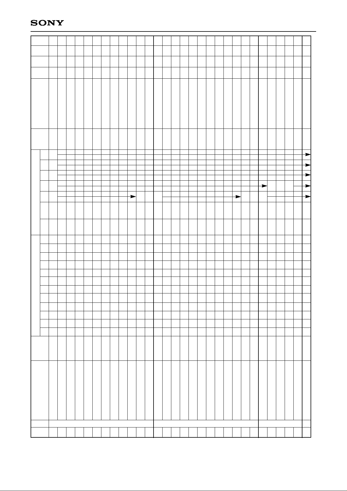
Electrical Characteristics (V
CC = 1.9V, VEE = –1.9V)
Page 8
– 8 –
CXA2570N
31
32
33
34
35
36
37
38
39
40
41
42
43
44
45
46
47
48
49
50
51
52
53
54
55
56
57
58
59
60
Offset voltage ROM
Offset voltage RW
Low-frequency gain ROM1
Low-frequency gain ROM2
Low-frequency gain RW1
Low-frequency gain RW2
Frequency response ROM1
Frequency response ROM2
Frequency response RW1
Frequency response RW2
Maximum output voltage H
Maximum output voltage L
Offset voltage ROM
Offset voltage RW
Low-frequency gain ROM1
Low-frequency gain ROM2
Low-frequency gain RW1
Low-frequency gain RW2
Frequency response ROM1
Frequency response ROM2
Frequency response RW1
Frequency response RW2
Maximum output voltage H
Maximum output voltage L
Output voltage 1
Output voltage 2
Output voltage 3
APC OFF voltage
Maximum output current
Output voltage
FE_OfstROM
FE_OfstRW
Gfe_ROM1
Gfe_ROM2
Gfe_RW1
Gfe_RW2
Ffe_ROM1
Ffe_ROM2
Ffe_RW1
Ffe_RW2
Vfe_H
Vfe_L
TE_OfstROM
TE_OfstRW
Gte_ROM1
Gte_ROM2
Gte_RW1
Gte_RW2
Fte_ROM1
Fte_ROM2
Fte_RW1
Fte_RW2
Vte_H
Vte_L
Vapc1
Vapc2
Vapc3
Vapc_off
Iapc_max
Vvc
O
O
O
O
O
O
O
O
O
O
O
O
O
O
O
O
O
O
O
O
O
O
O
O
O
O
O
O
O
O
O
O
O
O
O
O
O
O
O
O
O
O
O
O
O
O
Hi-Z
O
0.1Vp-p
0.1Vp-p
25mVp-p
25mVp-p
0.1Vp-p
0.1Vp-p
25mVp-p
25mVp-p
0.1Vp-p
0.1Vp-p
25mVp-p
25mVp-p
0.1Vp-p
0.1Vp-p
25mVp-p
25mVp-p
10kHz
10kHz
10kHz
10kHz
100kHz
100kHz
50kHz
50kHz
10kHz
10kHz
10kHz
10kHz
200kHz
200kHz
200kHz
200kHz
0V
0.3V
–0.3V
0V
0.3V
–0.3V
0V
0V
–
30mV
30mV
0V
0V 0V 0V 14
14
14
14
14
14
14
14
14
14
14
14
16
16
16
16
16
16
16
16
16
16
16
16
1
1
1
1
1
22
–150
–150
13.0
13.0
25.0
25.0
–3.5
–3.5
–3.5
–3.5
1.2
—
–150
–150
17.0
17.0
29.0
29.0
–1.5
–1.5
–4.5
–4.5
1.2
—
85
0.45
–
0.95
1.4
–
0.2
–
100
0
0
16.0
16.0
28.0
28.0
–0.5
–0.5
–0.5
–0.5
1.7
–1.5
0
0
20.0
20.0
32.0
32.0
0
0
–2.0
–2.0
1.7
–1.5
135
0.7
–
0.7
1.6
0
0
150
150
19.0
19.0
31.0
31.0
0.3
0.3
0.3
0.3
—
–1.1
150
150
23.0
23.0
35.0
35.0
1.5
1.5
–0.2
–0.2—–1.1
185
0.95
–0.45
–
0.6
100
mV
mV
dB
dB
dB
dB
dB
dB
dB
dB
V
V
mV
mV
dB
dB
dB
dB
dB
dB
dB
dB
V
V
mV
V
V
V
V
mV
Pin voltage
Pin voltage
20 log (Vout/Vin)
20 log (Vout/Vin)
20 log (Vout/Vin)
20 log (Vout/Vin)
20 log (Vout/Vin) – Gfe_ROM1
20 log (Vout/Vin) – Gfe_ROM2
20 log (Vout/Vin) – Gfe_RW1
20 log (Vout/Vin) – Gfe_RW2
Pin voltage
Pin voltage
Pin voltage
Pin voltage
20 log (Vout/Vin)
20 log (Vout/Vin)
20 log (Vout/Vin)
20 log (Vout/Vin)
20 log (Vout/Vin) – Gte_ROM1
20 log (Vout/Vin) – Gte_ROM2
20 log (Vout/Vin) – Gte_RW1
20 log (Vout/Vin) – Gte_RW2
Pin voltage
Pin voltage
Input where output voltage = 0V
Pin voltage
Pin voltage
Pin voltage
Pin voltage
Pin voltage
FETE
Measure-
ment No.
Function
Measurement item Symbol
Switch conditions Bias conditions
V1 amplitude
V1 frequency
E1 E2 E3 E4
E5
Measure-
ment pin
Measurement
conditions
Min.
Typ.
Max. Unit
S1 S2 S3 S4 S5 S6 S7 S8 S9 S10 S11 S12
VC APC
Page 9
– 9 –
CXA2570N
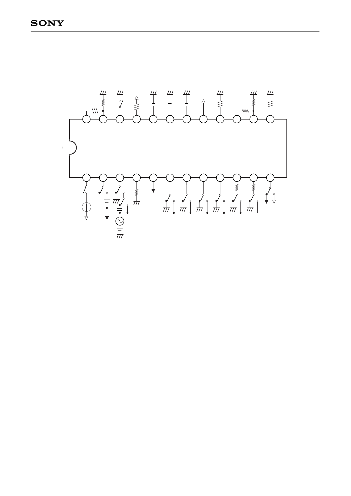
Electrical Characteristics Measurement Circuit
1 2
3
4 5
6
7 8 9 10 11 12
5.1k
5.1k
E5
S12
10k
V
CC
VCC
1.9V
10k
100k
10k
10k
S11
V
EE VCC
VEE
–1.9V
V
EEVCC
LD
PD
EQ_ IN
AC_SUM
GND
A
B
C
D
E
F
SW
RFDCI
RFDCO
VC
RFC
VFC
BST
RFG
V
CC
TE
FEI
FE
RFAC
0.1µ
10k
E1
V1
10k
E3E4
S10S9S8S7S6
S3
10k
S5
E2
0.8mA
S2S1
131415161718
19
2021
22
2324
Page 10
– 10 –
CXA2570N
Application Circuits
1 2
3
4 5
6
7 8 9 10 11 12
RFDC
OUT
TE
OUT
RFAC
OUT
5.1k
5.1k
20k
VC
V
CC VCC
FE
OUT
100k
10k
MODE
Control
DCBA
F
PD IN
LD
PD
EQ_ IN
AC_SUM
GND
A
B
C
D
E
F
SW
RFDCI
RFDCO
VC
RFC
VFC
BST
RFG
V
CC
TE
FEI
FE
RFAC
0.1µ
LD
Drive
RF
SUM
10k
E
20k 20k
1314
15
1617
18
19
2021
22
23
24
0.1µ
1 2
3
4 5
6
7 8 9 10 11 12
RFDC
OUT
TE
OUT
RFAC
OUT
5.1k
5.1k
20k
VC
V
CC VCC
FE
OUT
100k
10k
MODE
Control
DCBA
F
PD IN
LD
PD
EQ_ IN
AC_SUM
GND
A
B
C
D
E
F
SW
RFDCI
RFDCO
VC
RFC
VFC
BST
RFG
V
CC
TE
FEI
FE
RFAC
0.1µ
LD
Drive
10k
E
20k 20k
1314
15
1617
18
19
2021
22
23
24
0.1µ
Application circuits shown are typical examples illustrating the operation of the devices. Sony cannot assume responsibility for
any problems arising out of the use of these circuits or for any infringement of third party patent and other right due to same.
Page 11

– 11 –
CXA2570N
Description of Functions
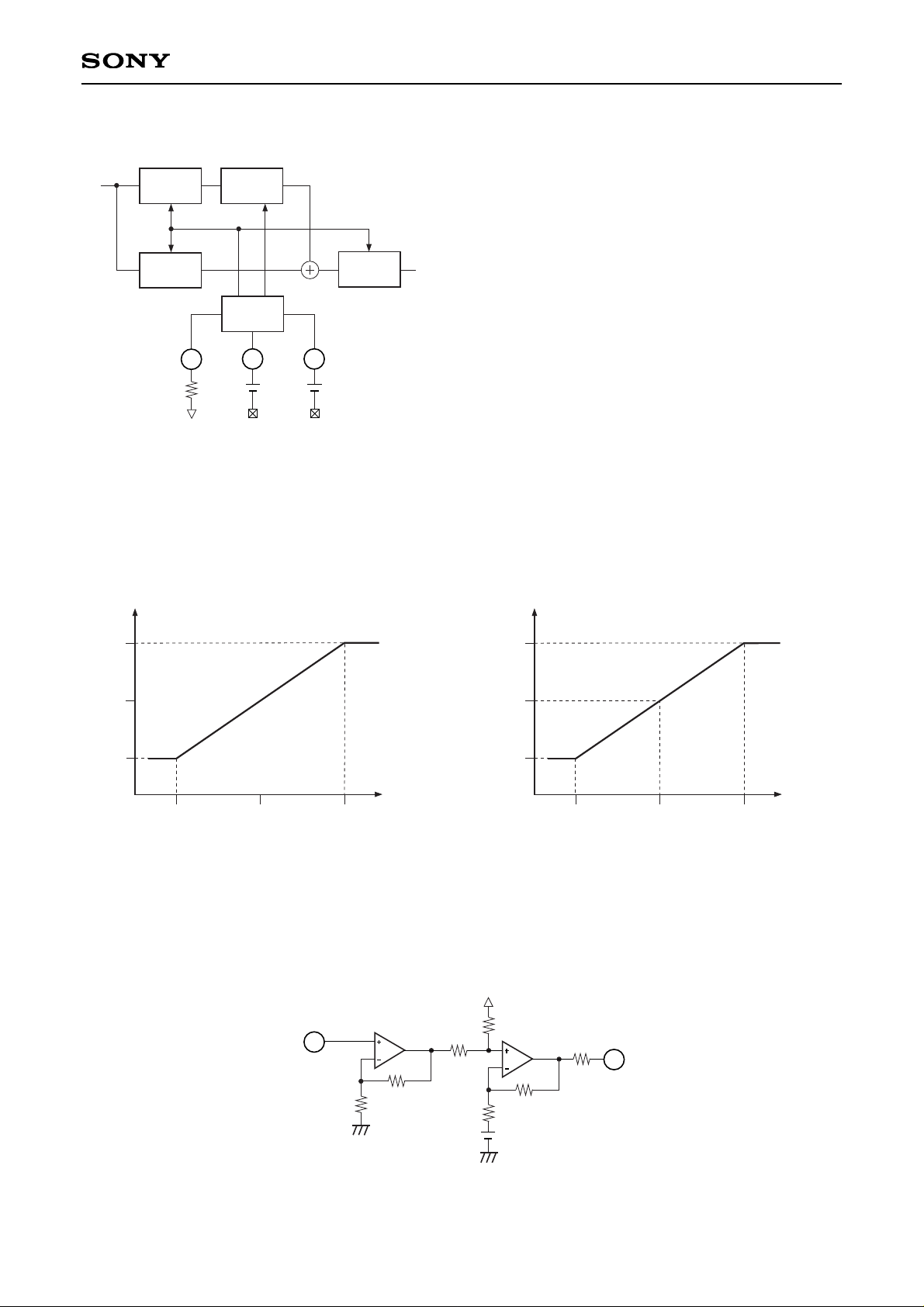
• RFAC
The RF signal input by connecting capacitance to the EQ_IN pin is equalized, arithmetically amplified and then
output from the RFAC pin.
19
20
13
3
4
6
7
8
9
18
A
B
C
D
AC_SUM
RW/ROM
EQ
AC
SUM
Amp
RFAC
VFCBST
EQ_IN
RFG
RF
When BST = VCC
21
VCC
RFC
5.1k
0.1
The EQ can be bypassed by connecting the BST control pin (Pin 19) to VCC. In this case only the EQ block
enters sleep mode and the low power consumption mode (slim mode) is activated. The low-frequency gain is
the same value as for EQ ON mode.
The RF_SUM input dynamic range is VC ± 300mV (typ.).
If RF (summing signal) is present at the pickup output pin, input the addition output signal to the EQ_IN pin
(Pin 3) coupled by capacitance.
When using a pickup without a summing output function, perform addition with the AC SUM block and then
input the signal to the EQ_IN pin coupled by capacitance.
RW/ROM switching is done by the VCA block, so either input method can be used without problem.
The RW gain is 12dB higher than the ROM gain.
The VCA low-frequency gain can be adjusted by
the RFG pin (Pin 18) voltage.
The control voltage vs. low-frequency gain
characteristics are shown in the graph to the right.
Gain [dB]
VC – 1
–8
0
8
VC
VCA variable range
VC + 1
Vcut [V]
The RFAC pin (Pin 13) is an NPN transistor emitter follower output.
The maximum drive current is approximately 2mA.
If the load capacitance distorts the output waveform, increase the drive current.
Connect resistance between Pin 13 and GND.
Low-frequency gain
AC_SUM: 16dB (both ROM/RW)
VCA to RFAC ROM: 2dB
RW: 14dB
Page 12
– 12 –
CXA2570N
The diagram to the left shows the EQ internal block
diagram.
The EQ consists of a combination of HPF and LPF.
The HPF and LPF transmittance is the Bessel function.
The boost gain can be adjusted by adjusting the HPF
gain.
The boost frequency is adjusted by the RFC external
resistance value and the VFC control voltage value.
RFC resistance value: The cut-off frequency fo of each
filter is adjusted by the Pin 21
external resistance value.
The VFC voltage can be varied
using this fo as the reference.
VFC voltage: fo can be changed by the voltage
applied to Pin 20.
• EQ
Boostfc
Amp
Out
RFC VFC
VCV
CC
BST
VC
In
HPF
LPF
EQ CNT
LPF
21
20
19
The boost gain can be adjusted by the BST pin
control voltage.
The control characteristics are shown in the graph
below.
The cut-off frequency control characteristics are
shown in the graph below.
Boost Gain [dB]
VC – 1.0
0dB
8dB
VC
Pin 19 voltage
VC + 1.0
Vcut [V]
fc [Hz]
VC – 1.0
0.5fo
fo
1.5fo
VC
Pin 20 voltage
VC + 1.0
Vcut [V]
• APC (Automatic Power Control)
When the laser diode is driven by a constant current, the optical power output has extremely large negative
temperature characteristics. Therefore, the current must be controlled to maintain the monitor photodiode
output at a constant level. This control is performed by the APC function
55k
LD
1k
10k
56k
56k
1.25V
10k
PD
10k
V
CC
2
1
Page 13

– 13 –
CXA2570N
• Focus Error
The signals input to the A and C pins and the B and D pins are arithmetically amplified and the focus error
signal is output.
This circuit has RW/ROM switching, low-frequency gain adjustment and offset adjustment (external resistance)
functions.
A
C
B
D
VC
200k50k
30k
50k
200k
RWROM
ROM
RW
VC
6
7
8
9
50k
FEFEI
R (ofst) 100k
15
14
FE = Gain {(B + D) – (A + C)}
Low-frequency gain ROM: 16dB
RW: 28dB
Cut-off frequency fc (typ.) ROM: 400kHz
RW: 300kHz
• Tracking Error
The signals input to the E and F pins are arithmetically amplified and the tracking error signal is output.
This circuit has RW/ROM switching, low-frequency gain adjustment and offset adjustment (external resistance)
functions.
ROM
ROM
RW
RW
TE
27k
10k
10k
373k
VC
10
11
27k
E
F
373k
16
TE = Gain (F – E)
Low-frequency gain ROM: 20dB
RW: 32dB
fc (typ.) ROM: 1MHz
RW: 250kHz
• VC Buffer
This outputs the VC ((1/2) VCC) voltage.
The maximum output current is approximately ±3mA.
25
V
CC VCC
40k
40k
22
Page 14

– 14 –
CXA2570N
• RFDC
The signals input via the A, B, C and D pins are added, amplified and the RFDC signal is output.
RW/ROM switching, low-frequency gain adjustment and offset adjustment are possible.
A
B
C
D
15k 10k
40k
ROM
RW
VC
VC
6
7
8
9
1.5k
RFDCORFDCI
5.1k
24
23
RFDC = Gain (A + B + C + D)
Low-frequency gain ROM: 20dB
RW: 32dB
fc (Typ.) ROM: 12MHz
RW: 5MHz
The gain can be adjusted by the external resistance connected between Pins 23 and 24.
• SW
This controls the laser (APC) on/off, active/sleep mode, and RW/ROM mode switching.
Switching is controlled by the voltage applied to the SW pin (Pin 12).
R (ofst)
SW RW/ROM, Active/Sleep, APC_ON/OFF
12
The VC buffer is kept active even in sleep mode.
In the function block, BGR and MODE_SW are always set to active mode.
Control voltage
Item
APC
ON
OFF
ON
Active
Sleep
Active
RW
—
ROM
VCC
VC or Hi-Z
GND
Active/Sleep RW/ROM
Page 15
– 15 –
CXA2570N
Notes on Operation
Stabilizing the RFAC signal
The RFAC system (RFSUM + EQ) is comprised entirely of non-inverted function blocks.
This is in order to support pickups with built-in RFSUM.
Therefore, if the voltage gain of each block is increased, a feedback loop is formed over the entire RFAC
system causing the RFAC signal to become unstable (oscillate).
In these cases, it is recommended to lower the EQ frequency response and the boost gain. This has a large
effect on the board (power supply, I/O signal cross talk, etc.) loop. The RFAC signal easily becomes unstable if
the VCA gain is increased, the EQ boost frequency is set to a high frequency, the EQ boost amount is
increased, etc.
The VCA gain is low in ROM mode, so the RFAC signal is stable. Also, when not using RFSUM, the RFAC
signal is stabilized because the overall gain is low.
The area where the RFAC signal becomes unstable is thought to vary for each set, as this is greatly affected
by the board loop as noted above.
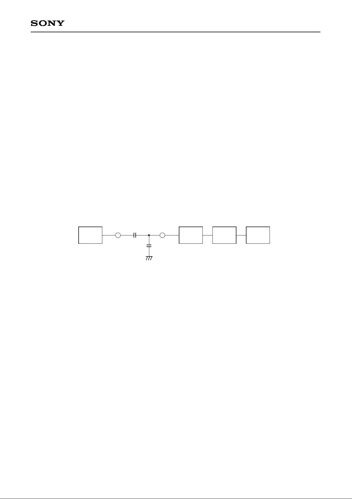
Proposed stabilization measures
The board and other loop characteristics can be changed by adding external capacitance as noted below.
This has a particularly large effect on the stabilization when using RFSUM.
RF
SUM
ACSUM EQI
Add capacitance of 10pF to 20pF.
0.1µ
VCA EQ AMP
Page 16

– 16 –
CXA2570N
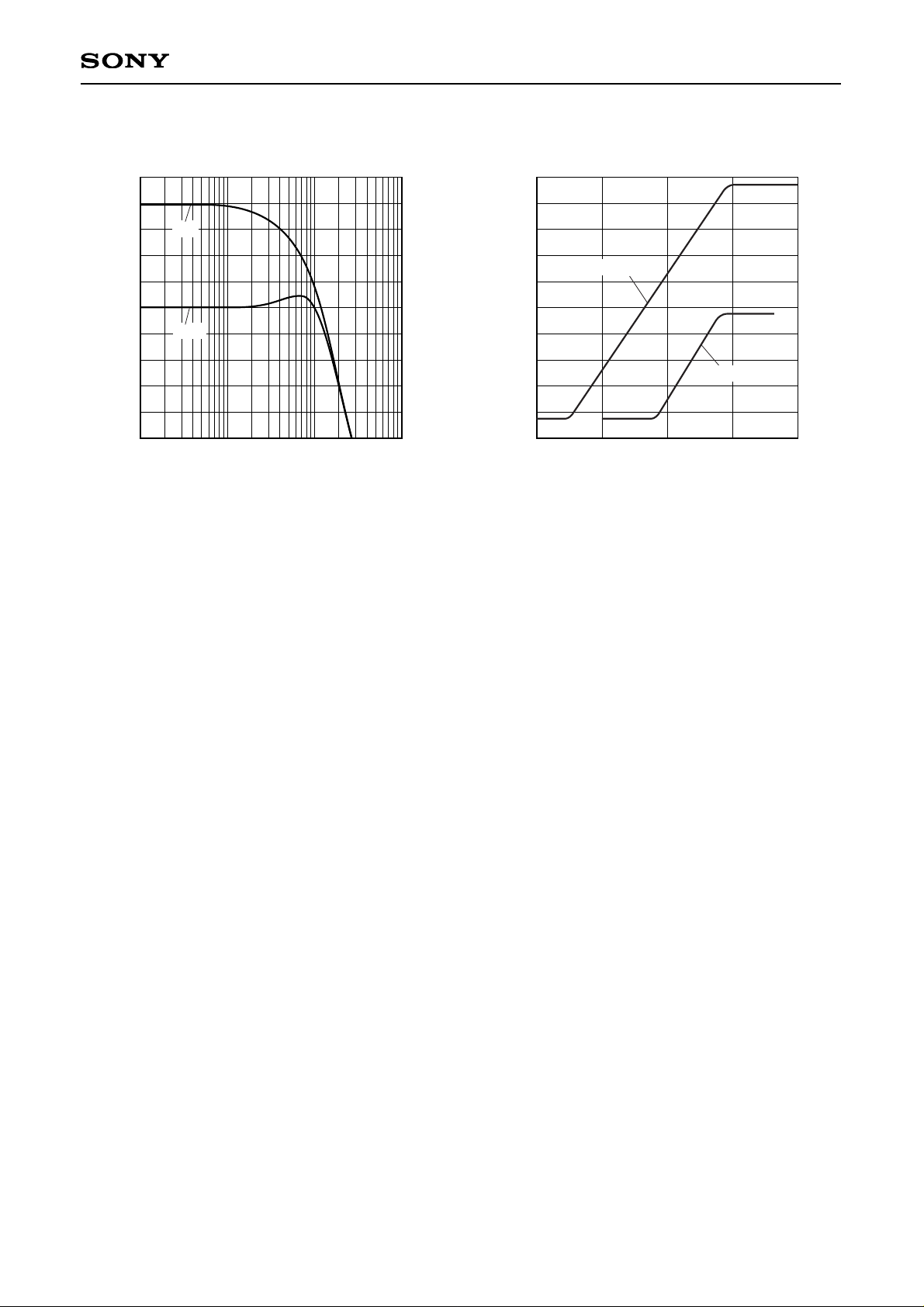
Example of Representative Characteristics
0
0.1
[MHz]
EQ Rfc resistance value – Frequency response
[dB]
1 10 100
1
2
3
4
5
6
7
8
9
10
Vbst = VC, Vfc = VC
Rfc = 100kΩ
Rfc = 20kΩ Rfc = 5.1kΩ
0
0.1
[MHz]
EQ Vfc frequency response
[dB]
1 10 100
1
2
3
4
5
6
7
8
9
10
Vbst = VC
Rfc = 20kΩ
Vfc = –1V
Rfc = 20kΩ
Vfc = 0V
Rfc = 20kΩ
Vfc = 1V
8
0.1
[MHz]
RF DC frequency response
[dB]
1 10 100
11
14
17
20
23
26
29
32
35
38
ROM
RW
4
0.01
[MHz]
FE frequency response
[dB]
0.1 1 10
7
10
13
16
19
22
25
28
31
34
ROM
RW
0.1
[MHz]
RF AC frequency response
[dB]
1 10 100
–7
–4
–1
2
5
8
11
14
17
20
EQ_Pass
RW mode
AC SUM
EQ_Pass
ROM mode
0.1
[MHz]
EQ boost voltage – Frequency response
[dB]
1 10 100
–4
–2
0
2
4
6
8
10
12
14
Vfc = VC
Rfc = 5.1kΩ
Vboost = 1.0V
Rfc = 5.1kΩ
Vboost = 0V
Rfc = 5.1kΩ
Vboost = –1.0V
Rfc = 100kΩ
Vboost = 0V
Rfc = 100kΩ
Vboost = –1.0V
Rfc = 100kΩ
Vboost = 1.0V
Page 17
– 17 –
CXA2570N
0.01
[MHz]
TE frequency response
[dB]
0.1 1 10
10
13
16
17
20
23
26
29
32
35
ROM
RW
0.05
VPD – Input voltage [V]
APC I/O characteristics
VLD – Output voltage [V]
0.1 0.15 0.2 0.25
1.0
0.5
1.5
2.0
2.5
3.0
3.5
4.0
4.5
5.0
5.5
VCC = 5.5V
VCC = 3.0V
Page 18

– 18 –
CXA2570N
Package Outline Unit: mm
SONY CODE
EIAJ CODE
JEDEC CODE
SSOP-24P-L01
SSOP024-P-0056
PACKAGE MATERIAL
LEAD TREATMENT
LEAD MATERIAL
PACKAGE MASS
EPOXY RESIN
SOLDER/PALLADIUM
42/COPPER ALLOY
PACKAGE STRUCTURE
PLATING
0.1g
24PIN SSOP(PLASTIC)
∗5.6 ± 0.1
24
∗7.8 ± 0.1
13
0.65
12
1
0.22 – 0.05
+ 0.1
0.15 – 0.02
+ 0.05
7.6 ± 0.2
0.1
1.25 – 0.1
+ 0.2
A
0.1 ± 0.1
0° to 10°
0.5 ± 0.2
DETAIL
A
NOTE: Dimensions “∗” does not include mold protrusion.
0.13
M
NOTE : PALLADIUM PLATING
This product uses S-PdPPF (Sony Spec.-Palladium Pre-Plated Lead Frame).
 Loading...