

Page 1
—1—
E97650A84-TE
Sony reserves the right to change products and specifications without prior notice. This information does not convey any license by
any implication or otherwise under any patents or other right. Application circuits shown, if any, are typical examples illustrating the
operation of the devices. Sony cannot assume responsibility for any problems arising out of the use of these circuits.
Absolute Maximum Ratings (Ta=25 °C)
• Supply voltage VCC –0.3 to 5.5 V
• Storage temperature Tstg –55 to +150 °C
Operating Conditions
• Supply voltage VCC 4.75 to 5.30 V
• Operating temperature Topr –25 to +75 °C
Description
The CXA3038N is an IC for IQ-detection of DSS,
DVB, and other digital satellite broadcast QPSK
modulation signals in the 480 MHz band. It consists
of an AGC amplifier circuit, oscillator circuit, phase
shifter circuit, and phase comparison circuit. In
addition, the chip has a PLL circuit for frequency
control and built-in control data. It realizes highaccuracy oscillator frequencies through use of a lowcost LC resonance circuit.
Features
• Built-in PLL for controlling oscillator frequency.
• Oscillator frequency based at 479.5 MHz is
adjustable in ±4 steps of 50 kHz using the voltage
of the control pin.
• Reference OSC allows switching to 4 MHz or 10
MHz.
• Built-in output buffer for reference OSC.
• Low-impedance IQ output.
• AGC gain variation 35 dB.
Applications
Digital satellite broadcast tuner
Structure
Bipolar silicon monolithic IC
IQ Detection IC for Digital Satellite Broadcast Tuner
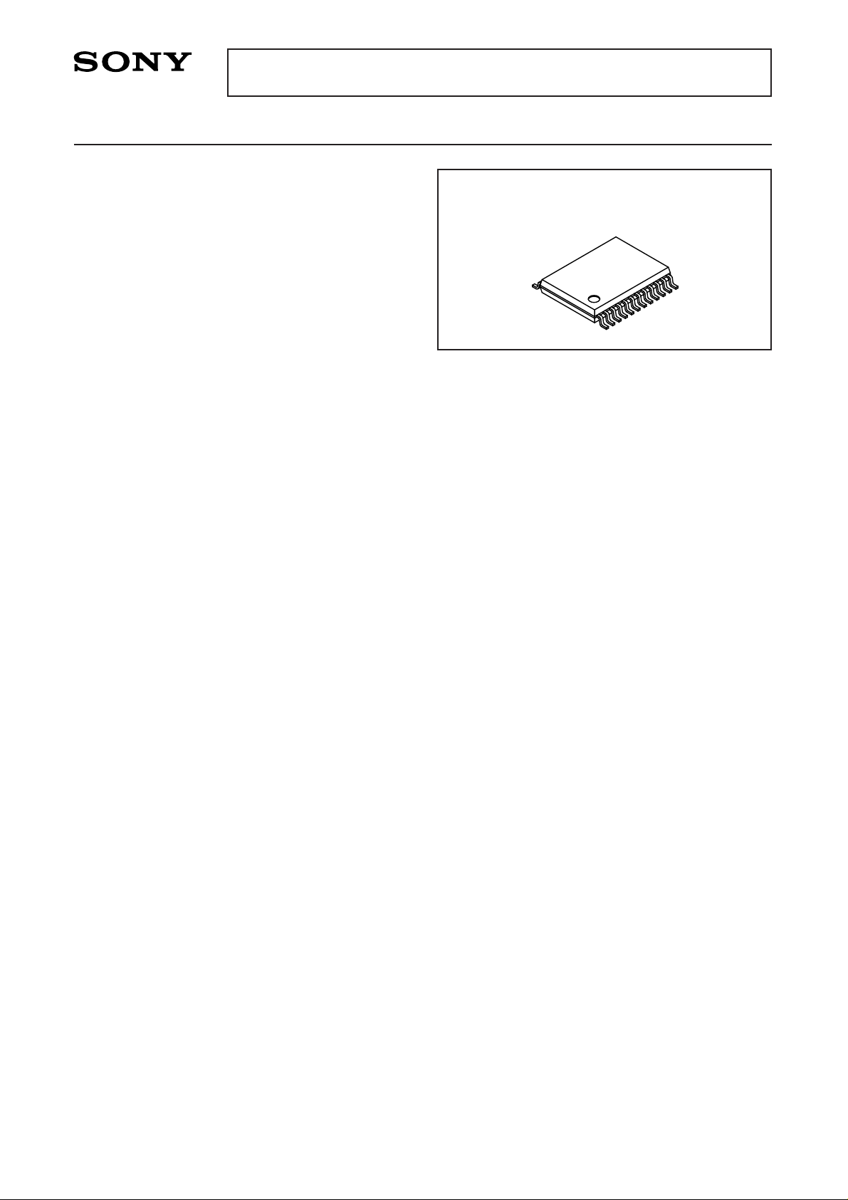
24 pin SSOP (Plastic)
CXA3038N
Page 2
—2—
CXA3038N
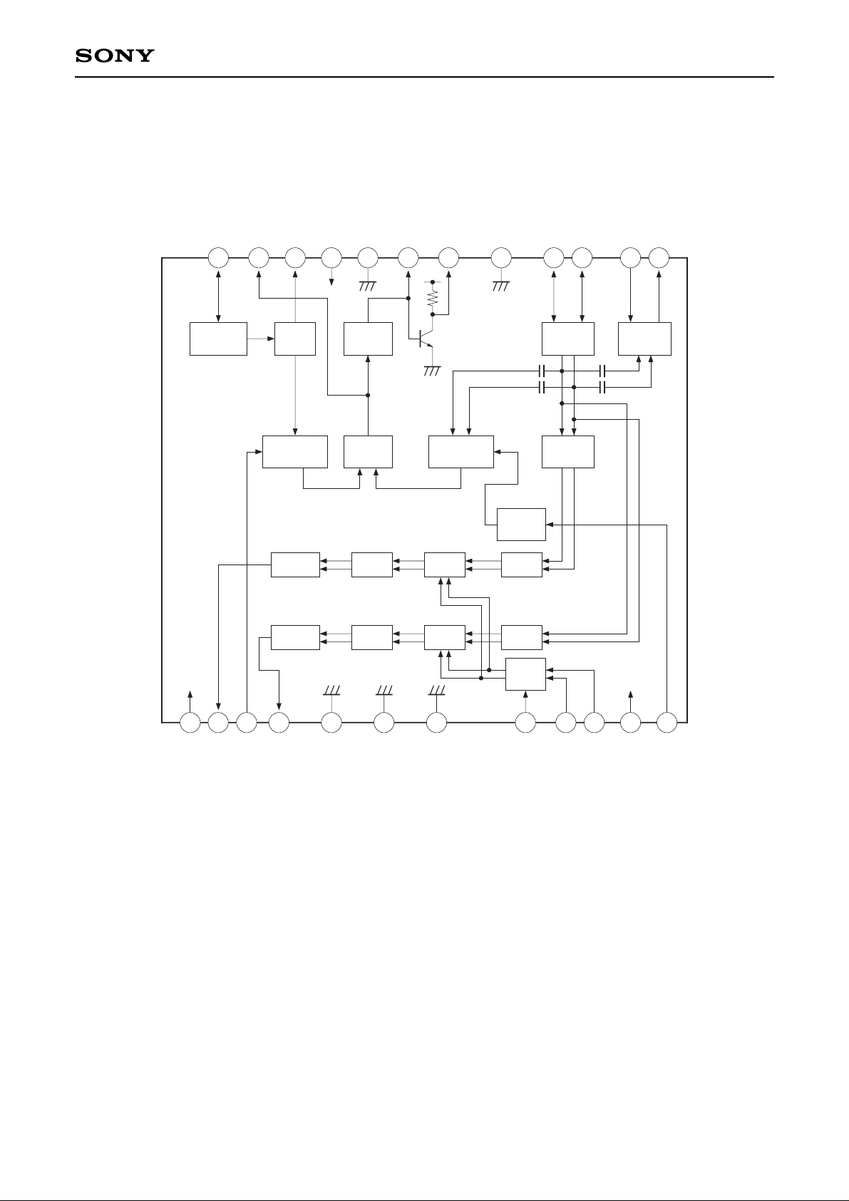
Block Diagram and Pin Configuration
Ref OSC Buffer
Charge
Pump
OSC
Prescaler
1/32
Divider
1/80, 1/200
Phase
DET
Divider
10bit+4bit
Phase
Shifter
Comparator
BufferLPFDC AMP
BufferLPFDC AMP
AGC
AMP
7 9
10
821 3 4 5 6
11 12
16 15 14 1324 23 22 21 20 19 18 17
XTAL
LOCK
REFOUT
DV
CC
DGND
LPF
VC
OSCGND
OSC1
OSC2
PSV
CC
LOOUT
IQV
CC
QOUT
XCONT
IOUT
IQGND
GND
RFGND
AGC
RFIN2
RFIN1
RFV
CC
NSET
IMIX
QMIX
Page 3
—3—
CXA3038N
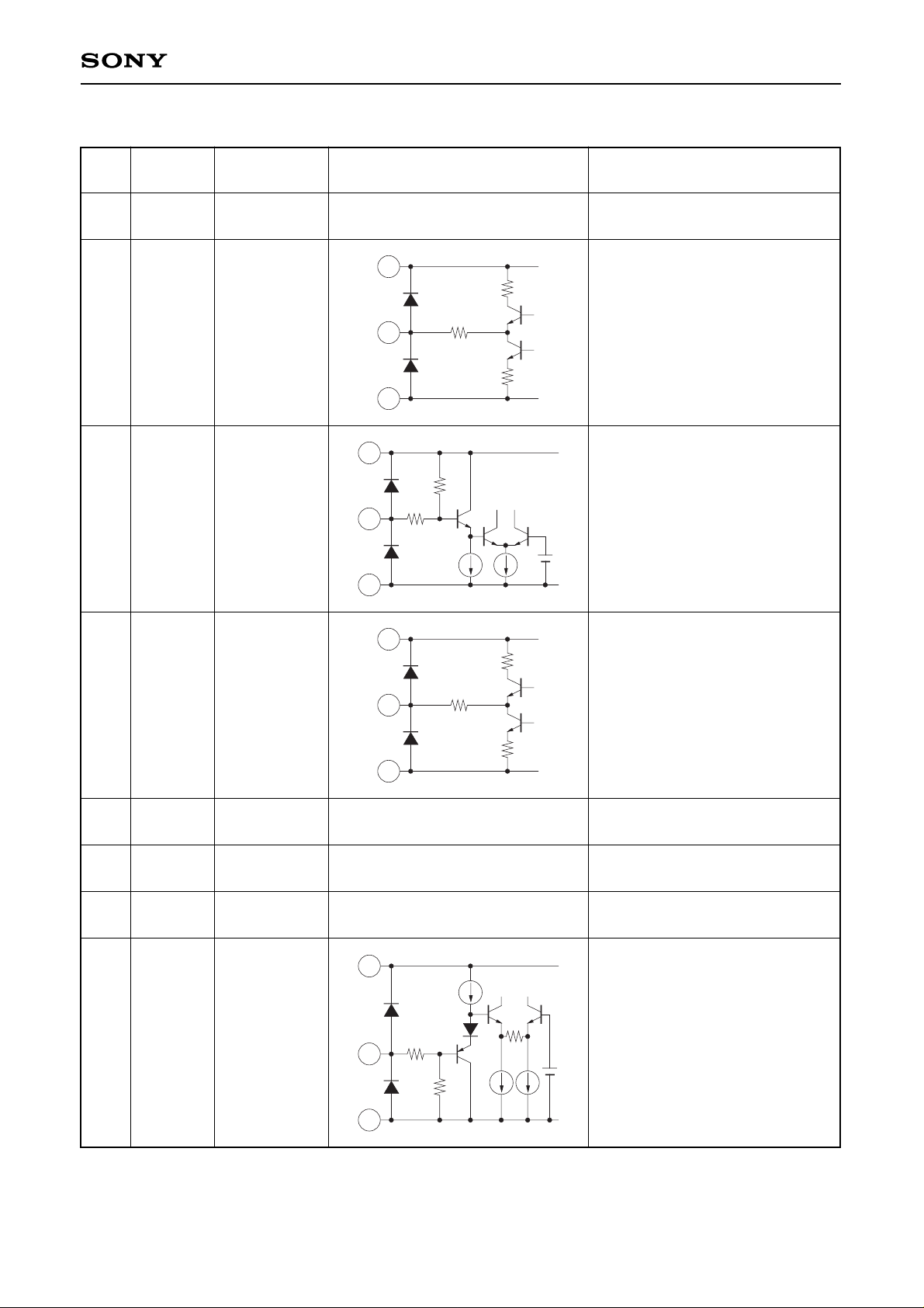
Pin Description
Pin
Symbol
Typical pin
Equivalent circuit Description
No. voltage
1
2
3
4
5
6
7
8
IQVCC
QOUT
XCONT
IOUT
IQGND
GND
RFGND
AGC
5 V
2.7 V
Open or 5 V
when using
4 MHz crystal ;
0 V when using
10 MHz crystal.
2.7 V
0 V
0 V
0 V
0 to 4 V
1
2
5
20
90k
21
3
20
10k
1
4
5
20
20k
20k
11
8
7
IQ output circuit VCC.
Q output.
Switching pin for reference divider
frequency-division ratio.
This is set to 80 frequency
divisions when open or connected
to VCC; 200 frequency divisions
when connected to GND.
I output.
IQ output circuit GND.
GND.
RF circuit (AGCAmp, MIXER)
GND.
AGCAmp gain adjustment.
Page 4
—4—
CXA3038N
Pin
Symbol
Typical pin
Equivalent circuit Description
No. voltage
9
10
11
12
13
14
15
16
17
RFIN2
RFIN1
RFVCC
NSET
LOOUT
PSVCC
OSC2
OSC1
OSCGND
2.1 V
2.1 V
5 V
1.6 V
4 V
5 V
3.7 V
3.7 V
0 V
5k
9
10
7
2.2V
5k
21
12
20
14
13
20
8k
11
17
16
15
700 700
3p
3p
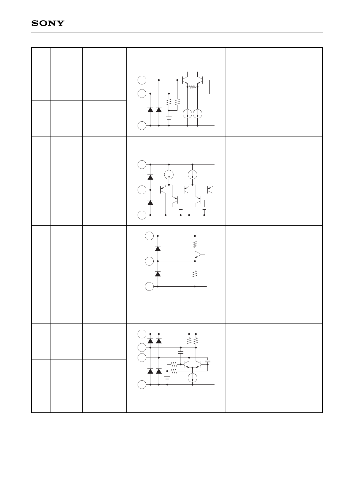
RF signal inputs.
RF circuit (AGCAmp, MIXER,
OSC) VCC.
OSC frequency fine-adjustment.
The oscillator frequency based at
479.5 MHz is adjustable in ±4
steps of 50 kHz by applying a
voltage of 0 to 5 V.
Output for OSC frequency signal
divided into 32 frequency divisions.
VCC for 32 frequency division
circuit. This is set to open when
activating the built-in PLL.
OSC pins.
These pins connect the varicap
diode and coil resonance circuit.
OSC circuit and phase shifter
circuit GND.
Page 5

—5—
CXA3038N
Pin
Symbol
Typical pin
Equivalent circuit Description
No. voltage
18
19
20
21
22
23
24
VC
LPF
DGND
DVCC
REFOUT
LOCK
XTAL
0.3 V to 5 V
1.8 V to 3.7 V
0 V
5 V
4.1 V
0.01 V when
unlocked; 3.2 V
when locked
4.4 V
100
21
18
20
10k
100
21
19
20
21
22
20
21
23
20
200k
21
20
24
60k
20p
20p
Voltage output for varicap diode
making up the VCO.
Phase comparison output.
This pin connects the loop filter.
PLL circuit GND.
PLL circuit VCC.
REFOSC output.
PLL lock/unlock monitor.
Crystal connection.
Page 6

—6—
CXA3038N
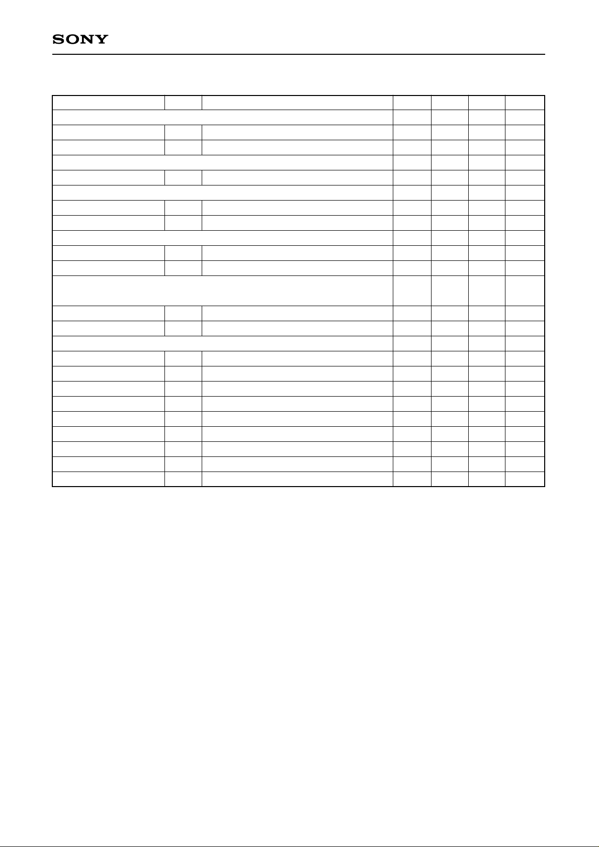
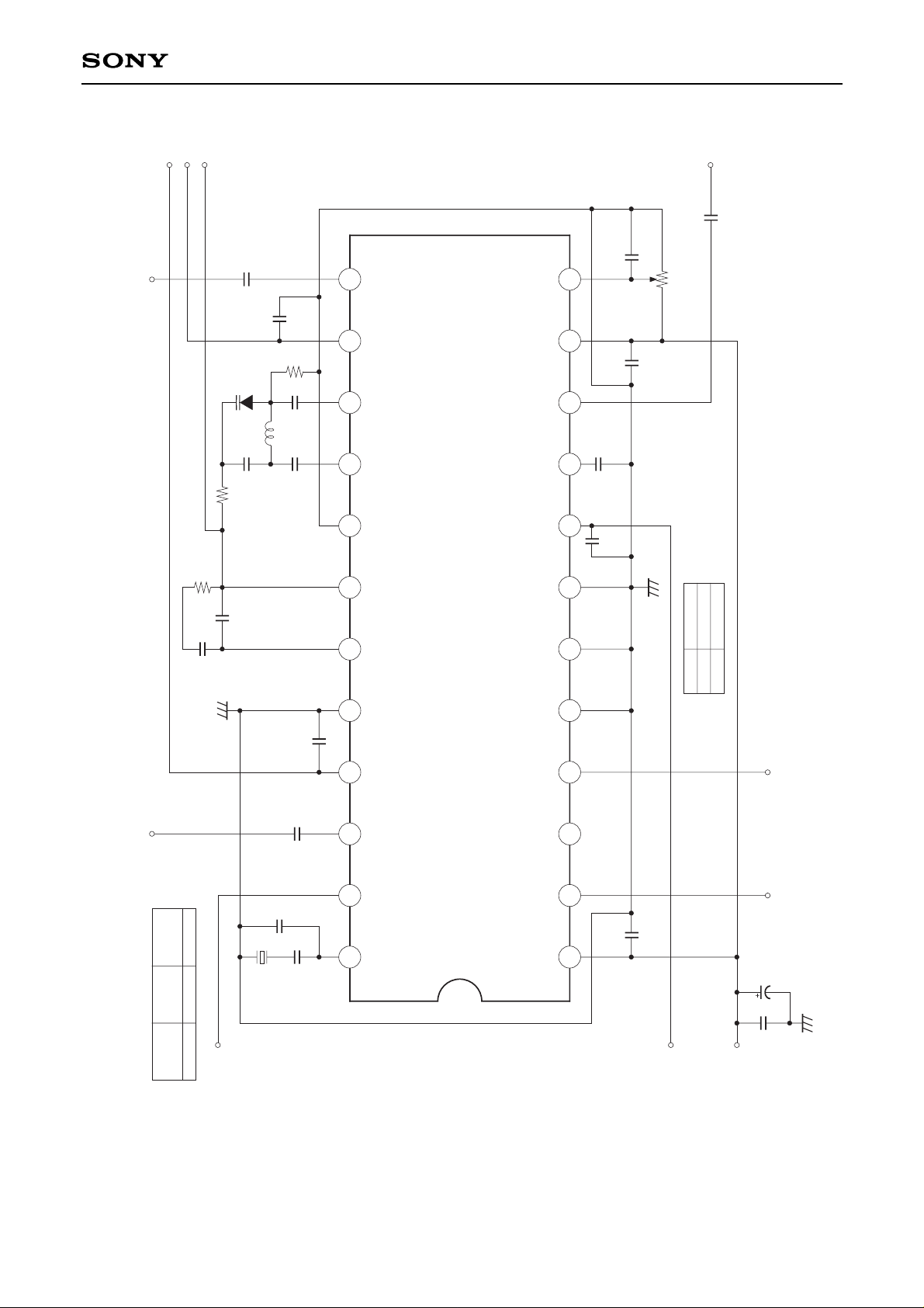
Electrical Characteristics
Circuit current (Ta=25 °C, VCC=5 V, see the Electrical Characteristics Measurement Circuit.)
Item Symbol Measurement conditions Min. Typ. Max. Unit
Circuit current A
Circuit current D
Circuit current L
ICCA
ICCD
ICCPS
Analog circuit current at no signal.
Total current of IQVCC and RFVCC.
PLL circuit current. DVCC current.
32-frequency division circuit current at no
signal. PSVCC current.
41 60 80 mA
2 3.5 5.5 mA
1.1 1.6 2.4 mA
AC Characteristics (Ta=25 °C, VCC=5 V, see the Electrical Characteristics Measurement Circuit.)
Item Symbol Measurement conditions Min. Typ. Max. Unit
Input sensitivity
Gain control range
Conversion gain
IQ phase error
IQ amplitude error
Phase frequency error
Amplitude frequency error
Cut-off frequency
Maximum Q output
Maximum I output
Noise figure
Third-order
intermodulation distortion
Local oscillation
phase noise
PLL reference leak
RF pin local
oscillation leak
QOUT pin local
oscillation leak
IOUT pin local
oscillation leak
REFout pin local
oscillation leak
RF input admittance
VIN
GAGC
CG
BP
BV
∆fBP
∆fBV
fC
VQMAX
VIMAX
NF
IM3
CN
refLK
RFLK
QLK1
QLK2
ILK1
ILK2
REFLK
rπ
Cπ
Iout=10 MHz, 1 Vp-p
Iout=10 MHz, 1 Vp-p, AGC=4 V-0 V
RF=–50 dBm, Iout=10 MHz, AGC=4 V
(Full gain)
RF=–50 dBm, Iout=10 MHz, 1 Vp-p
RF=–50 dBm, Iout=10 MHz, 1 Vp-p
RF=–50 dBm, Iout=0 MHz–15 MHz, 1 Vp-p
RF=–50 dBm, Iout=0 MHz–15 MHz, 1 Vp-p
RF=–50 dBm, Iout=From 1 Vp-p to 3 dB down
RF=–30 dBm, Qout=10 MHz, AGC=4 V
(Full gain)
RF=–30 dBm, Iout=10 MHz, AGC=4 V
(Full gain)
Iout=10 MHz, AGC=4 V (Full gain), DSB
RF1=489.5 MHz, RF2=490.5 MHz,
Iout=1 Vp-p
RF=–50 dBm, Iout=10 MHz, 1Vp-p,
10 kHz offset
RF=–50 dBm, Iout=10 MHz, 1Vp-p,
50 kHz S/I
AGC=4 V, f=479.5 MHz
AGC=4 V, f=479.5 MHz
AGC=0 V, f=479.5 MHz
AGC=4 V, f=479.5 MHz
AGC=0 V, f=479.5 MHz
f=479.5 MHz
f=479.5 MHz, AGC=4 V (Full gain)
–50 dBm
32.5 35 — dB
52 54 57 dB
±4 deg
±0.5 dB
±0.5 deg
±0.1 dB
25 MHz
2.5 3 3.5 Vp-p
2.5 3 3.5 Vp-p
9 dB
32 dB
–88 dBc/Hz
–81 dB
–21 dBm
–34
dBm
–40
–34
dBm
–40
–34 dBm
1.25 k Ω
1.4 pF
Measured value for untuned inputs.
Noise figure is the direct reading value from the NF meter.
Page 7
—7—
CXA3038N
PLL Block (Ta=25 °C, VCC=5 V, see the Electrical Characteristics Measurement Circuit.)
Item Symbol Measurement conditions Min. Typ. Max. Unit
LPF (charge pump)
H output current
L output current
VC
Output voltage range
LOCK
H output voltage
L output voltage
REFOUT
Output frequency
Output amplitude
LOOUT
(32 frequency divisions)
Output frequency
Output amplitude
OSC control
479.7 MHz control voltage
479.65 MHz control voltage
479.6 MHz control voltage
479.55 MHz control voltage
479.5 MHz control voltage
479.45 MHz control voltage
479.4 MHz control voltage
479.35 MHz control voltage
479.3 MHz control voltage
ILPFH
ILPFL
VVCH
VLH
VLL
fREF
VREF
fLO
VLO
f+4
f+3
f+2
f+1
f0
f–1
f–2
f–3
f–4
XCONT=OPEN, PLL lock
XTAL=4 MHz, XCONT=OPEN, PLL lock
XTAL=4 MHz, XCONT=GND, PLL unlock
XTAL=4 MHz
XTAL=4 MHz
OSC=479.5 MHz during PLL lock
OSC=479.5 MHz during PLL lock
NSET=0 V, f0 V–f0=f∆4
NSET=0.4 V, f0.4 V–f0=f∆3
NSET=0.8 V, f0.8 V–f0=f∆2
NSET=1.2 V, f1.2 V–f0=f∆1
NSET=1.6 V
NSET=2.0 V, f2.0 V–f0=f∆–1
NSET=2.4 V, f2.4 V–f0=f∆–2
NSET=2.6 V, f2.6 V–f0=f∆–3
NSET=3.2 V, f3.2 V–f0=f∆–4
–50 µA
50 µA
0.3 VCC V
2.8 3.2 4.2 V
0 0.01 0.2 V
4.000 MHz
230 280 400 mVp-p
14.9844 MHz
300 380 500 mVp-p
0.597 VCC
VCC V
0.517 VCC 0.590 VCC
V
0.438 VCC 0.515 VCC
V
0.358 VCC 0.436 VCC
V
0.279 VCC 0.356 VCC
V
0.199 VCC 0.277 VCC
V
0.120 VCC 0.197 VCC
V
0.042 VCC 0.118 VCC
V
0
0.04 VCC
V
Page 8
—8—
CXA3038N
Electrical Characteristics Measurement Circuit
XTAL
LOCK
REFOUT
DV
CC
DGND
LPF
VC
OSCGND
OSC1
OSC2
PSV
CC
LOOUT
IQV
CC
QOUT
XCONT
IOUT
IQGND
GND
RFGND
AGC
RFIN2
RFIN1
RFV
CC
NSET
10n 4MHz
2p
REFOUT
10n
1n
680n
13k
150n
51k
5p
1n
L
80nH
1T362
1n
51k
DVCC (+5V)
PSV
CC (+5V)
VC
1n
10n
LOOUT
XTAL
23 22 21 19 18 17 16 15 14 1324 20
CXA3038N
QOUT IOUT
1n
1n
1n 1n
100k
1n
1n
LOCK
AGC
7 9
10
821 3 4 5 6
11 12
XTAL
4MHz
10MHz
XCONT
5V/OPEN
GND
VCC (+5V)
1n
10µ
RF IN
0.5 3.0 2.5
L: Inductance constant
Wire
diameter
Winding
diameter
Number
of turns
Page 9

—9—
CXA3038N
Application Circuit
XTAL
LOCK
REFOUT
DV
CC
DGND
LPF
VC
OSCGND
OSC1
OSC2
PSV
CC
LOOUT
IQV
CC
QOUT
XCONT
IOUT
IQGND
GND
RFGND
AGC
RFIN2
RFIN1
RFV
CC
NSET
10n 4MHz
2p
REFOUT
10n
1n
680n
13k
150n
51k
5p
1n
L
80nH
1T362
1n
51k
XTAL
CXA3038N
QOUT IOUT
VCC (+5V)
1n
10µ
RF IN
L ; 0.5/3.0/2.5T
Reference Clock for
Tuner stage PLL.
23 22 21 19 18 17 16 15 14 1324 20
1n
AGC
1n
1n
1n
68k 33k
1n
479.5MHz
from Tuner stage
7 9
10
821 3 4 5 6
11 12
Application circuits shown are typical examples illustrating the operation of the devices. Sony cannot assume responsibility for
any problems arising out of the use of these circuits or for any infringement of third party patent and other right due to same.
Page 10
—10—
CXA3038N
Description of Operation
(See the Electrical Characteristics Measurement Circuit.)
Oscillator circuit
• This is a differential amplification-type oscillator circuit, and it is oscillated by connecting an LC parallel
resonance circuit via a coupling capacitance between Pin 15 and Pin 16.
A varicap diode is used as a capacitor for the LC parallel resonance circuit to configure the VCO. Set the L
value so that the OSC oscillation frequency is approximately 480 MHz when a voltage of 2.5 V is applied to
the varicap diode.
• The oscillator signal is injected into the phase shifter circuit.
Phase shifter circuit
• This is a phase shifter having CR configuration.
This circuit produces two local signals having a 90° phase difference at 479.5 MHz and injects these signals
to the IQ mixer circuit.
AGC amplifier circuit
• An IF signal (480 MHz band) from the tuner stage is input to Pins 9 and 10.
This IF signal which is input to Pins 9 and 10 is amplified by the AGC amplifier and injected into the IQ mixer
circuit.
• The gain can be adjusted by applying the AGC voltage to Pin 8.
The applied AGC voltage ranges from 0 to 4 V, with the minimum gain at 0 V and the maximum gain at 4 V.
IQ mixer circuit
• This is a double-balance mixer-type circuit consisting of two mixer circuits.
• The IF signal amplified by the AGC amplifier is converted into a base band signal by the local signal.
Low-pass filter circuit
• This is a low-pass filter with a CR configuration.
• The cut-off frequency is set at 25 MHz (–3 dB point).
Output amplifier circuit
• The signal is converted to a base band signal by the I and Q mixer circuits, and the high-frequency
component is removed by the low-pass filter. This signal is then amplified by the output amplifier circuit and
output to Pin 2 as a Q signal. In the same way, the I signal is output to Pin 4.
• The output is low impedance.
Page 11

—11—
CXA3038N
PLL circuit (when Pin 21 is connected to VCC)
• A PLL is formed by connecting the anode of the LC parallel resonance circuit varicap diode to the Pin 18
output via a high resistance of approximately 10 kΩ and connecting a loop filter between Pin 18 and Pin 19.
• The PLL circuit consists of a main divider, reference divider, phase comparator, charge pump, and reference
oscillator.
• The frequency dividing data is included in the main divider, making external data settings unnecessary.
• The reference frequency has been designed at 50 kHz.
• Fine adjustment of the VCO frequency can be performed by changing the frequency dividing value of the
main divider through an applied voltage to Pin 12. This allows adjustment in ±4 steps at 50 kHz intervals
based at 479.5 MHz as shown in the table below.
• The reference divider has two types of frequency dividing data, 80 and 200.
• Either 4 MHz or 10 MHz can be selected for the crystal oscillator. When using the 4 MHz crystal oscillator,
opening Pin 3 will select a frequency dividing value of 80 for the reference divider, and the reference
frequency will become 50 kHz.
In the same way, when using the 10 MHz crystal oscillator, connecting Pin 3 to GND will select a frequency
dividing value of 200 for the reference divider, and the reference frequency will become 50 kHz.
This is summarized in the table below.
Pin 12 voltage [V]
0.597 VCC or more
0.517VCC to 0.595VCC
0.438VCC to 0.515VCC
0.358VCC to 0.436VCC
0.279VCC to 0.356VCC
0.199VCC to 0.277VCC
0.120VCC to 0.197VCC
0.042VCC to 0.118VCC
0 to 0.04VCC
Frequency dividing value
9594
9593
9592
9591
9590
9589
9588
9587
9586
VCO oscillation frequency [MHz]
479.70
479.65
479.60
479.55
479.50
479.45
479.40
479.35
479.30
Crystal
oscillator
4 MHz
10 MHz
Pin 3 voltage
Open
0.8 V or less
Frequency dividing value
of the reference divider
80
200
Reference frequency
50 kHz
50 kHz
Page 12
—12—
CXA3038N
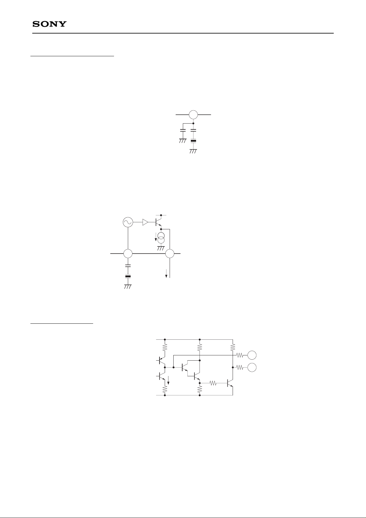
Reference oscillator circuit
• This is oscillated by connecting a crystal oscillator (4 MHz or 10 MHz) between Pin 24 and GND.
• The input capacitance of Pin 24 is approximately 14 pF. Therefore, a crystal with a load capacitance of 12
pF is recommended. When connecting a crystal with a large load capacitance of 16 pF or so, connect a low
capacitance between Pin 24 and GND as shown in the figure below, and adjust the frequency.
• The reference oscillator signal is sent to the reference buffer circuit and output from Pin 22 by the emitter
follower. The reference oscillator signal becomes the PLL comparison frequency in the IC.
• The output amplitude is approximately 300 mVp-p.
Charge pump circuit
• The output current of the charge pump has been designed at 50 µA.
• The Pin 18 output voltage ranges from approximately 0.3 V to VCC.
• In the loop filter example for the Electrical Characteristics Measurement Circuit, the lockup time is
approximately 25 ms.
24
Crystal oscillator
4MHz or 10MHz
Capacitance of DC
components eliminated
Reference frequency
fine-adjustment capacitance
24 22
200µA
Usage as PLL reference frequency for the tuner block
1k
1k
1k
20k
500
19
100
18
100
50µA
DVCC
DGND
10k
From phase divider
From main divider
Page 13

—13—
CXA3038N
32 frequency division circuit (when Pin 14 is connected to VCC)
• An oscillation signal is sent from the oscillator circuit to the 32 frequency division circuit via a coupling
capacitance. The 32 frequency division signal is output from Pin 13 by the counter.
• The output is approximately 400 mVp-p ECL output.
Notes on Operation
• These circuits use high-frequency processes, and the electrostatic strength is weak.
Therefore, please be careful of surges and other excessive input.
• The IQ error may vary depending on the connection locations of the GND pattern and VCC-GND bypass
capacitors, oscillation amplitude of the oscillator circuit, and other factors.
Page 14

—14—
CXA3038N
NF [dB]
RF input level vs. Phase difference
IQ output frequency=1MHz, QOUT=1Vp-p
Phase difference [deg]
RF input level [dBm]
RF input level vs. Amplitude error
IQ output frequency=1MHz, QOUT=1Vp-p
Amplitude error [dB]
RF input level [dBm]
IQ output frequency vs. Phase difference
RF input level=–40dBm, QOUT=1Vp-p
Phase difference [deg]
IQ output frequency [MHz]
IQ output frequency vs. Amplitude error
RF input level=–40dBm, QOUT=1Vp-p
Amplitude error [dB]
IQ output frequency [MHz]
Supply voltage vs. Current consumption
During PLL operation
Current consumption [mA]
Supply voltage [V]
Noise figure characteristics
RF input level=–40dBm, QOUT=10MHz
AGC voltage [V]
95
94
93
92
91
90
89
88
87
86
85
–60 –55 –50 –45 –40 –35 –30 –25 –20 –15 –10
2
1.5
1
0.5
0
–0.5
–1
–1.5
–2
–60 –55 –50 –45 –40 –35 –30 –20 –15 –10
95
94
93
92
91
90
89
88
87
86
85
0 2 4 6 8 10 12 14 16 18 20
2
1.5
1
0.5
0
–0.5
–1
–1.5
–2
0 2 4 6 8 10 12 14 16 18 20
90
80
70
60
50
30
40
4.2 4.4 4.6 4.8 5 5.2 5.4 5.6 5.8
35
30
25
20
15
10
5
0
0 0.5 1 1.5 2 2.5 3 3.5 4 4.5 5
–25
Page 15
—15—
CXA3038N
60
55
50
40
35
30
25
20
15
10
0 1 2 3 4
20
0
–60
–100–90 –80 –70 –60 –50 –40 –30 –20 –10 0
–50
–60
–70
–80
–90
–100
–120
C/N [dBc/Hz]
0.1 1 10 100 1000
5
45
–50
–40
–30
–20
–10
10
A
OSC=479.5MHz
RF1=498.5MHz
RF2=490.5MHz
AGC=4V
–110
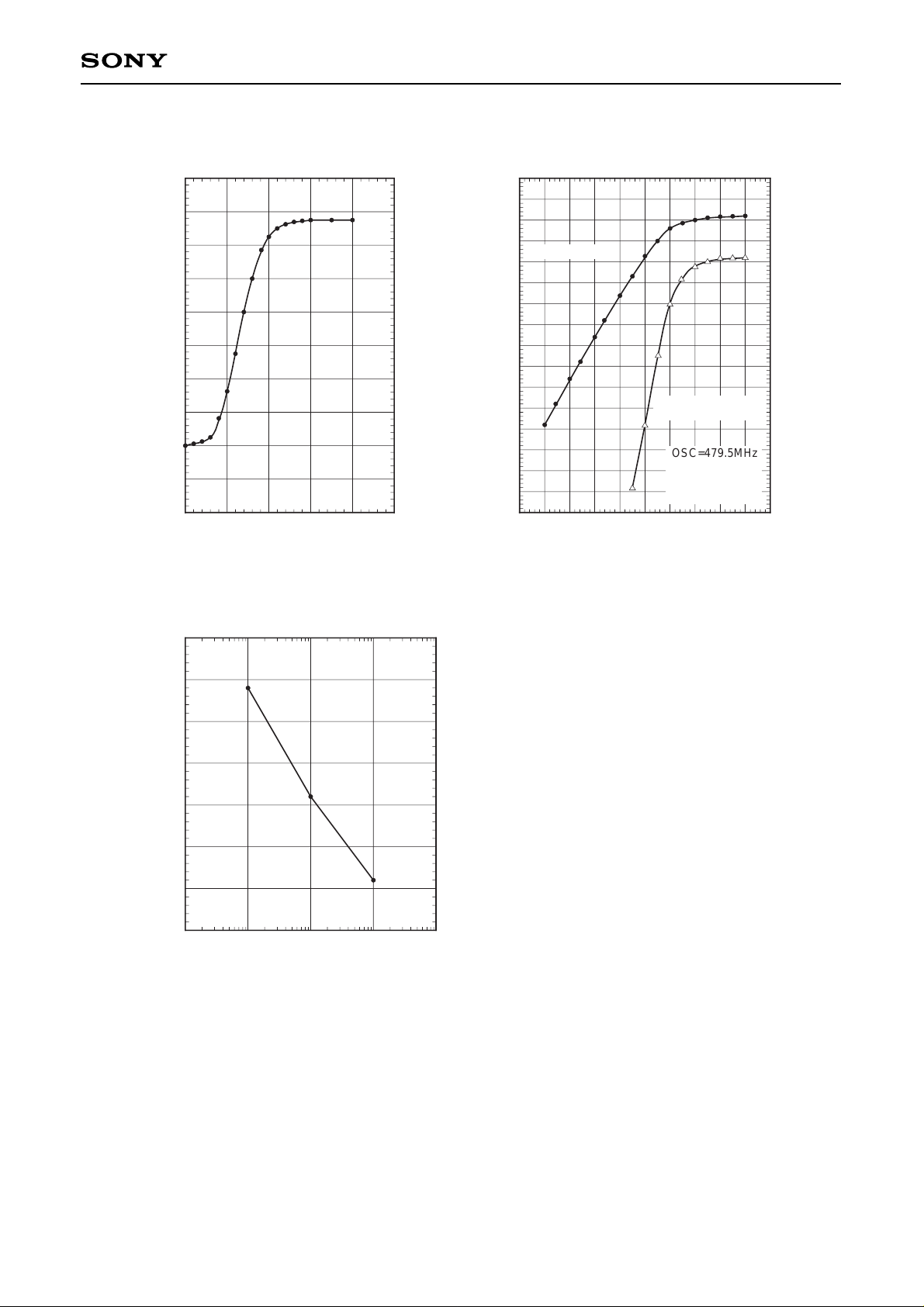
AGC voltage vs. Gain
RF input level=–40dBm, IQ output frequency=1MHz
Gain [dB]
AGC voltage [V]
Third-order intermodulation distortion characteristics
QOUT output level [dBm]
RF input level [dBm]
Fundamental
Third-order intermodulation
distortion component
Phase noise characteristics
RF input level=–40dBm, QOUT=1 MHz, 1Vp-p
Offset frequency [kHz]
AA
Page 16
∗5.6 ± 0.1
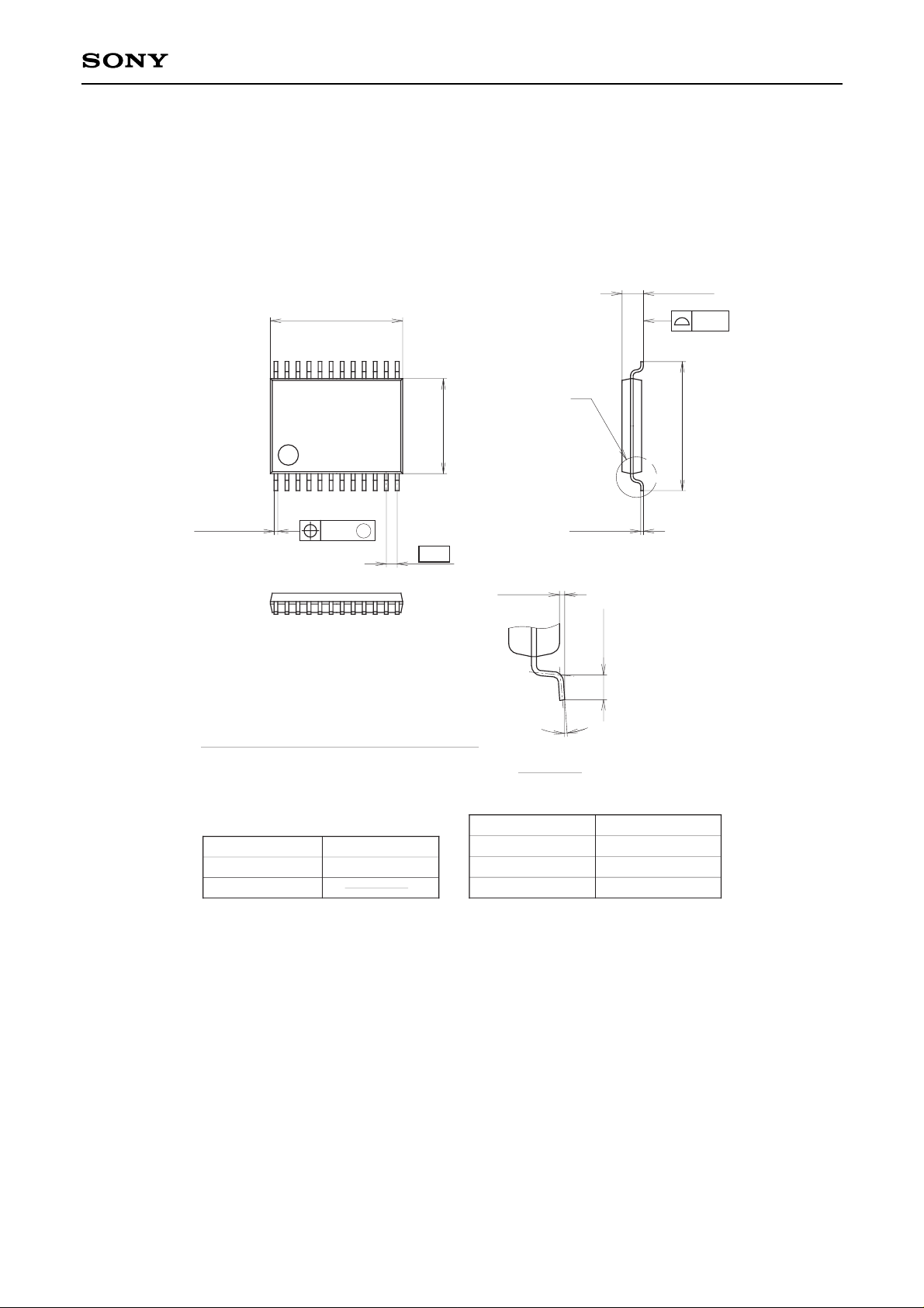
Package Outline Unit : mm
∗7.8 ± 0.1
24PIN SSOP(PLASTIC)
+ 0.2
1.25 – 0.1
CXA3038N
0.1
24
1
+ 0.1
0.22 – 0.05
NOTE: Dimensions “∗” does not include mold protrusion.
0.13
13
12
M
0.65
0.1 ± 0.1
0° to 10°
DETAIL
A
+ 0.05
0.15 – 0.02
0.5 ± 0.2
A
7.6 ± 0.2
SONY CODE
EIAJ CODE
JEDEC CODE
SSOP-24P-L01
SSOP024-P-0056
NOTE : PALLADIUM PLATING
This product uses S-PdPPF (Sony Spec.-Palladium Pre-Plated Lead Frame).
PACKAGE STRUCTURE
PACKAGE MATERIAL
LEAD TREATMENT
LEAD MATERIAL
PACKAGE MASS
—16—
EPOXY RESIN
SOLDER/PALLADIUM
42/COPPER ALLOY
0.1g
PLATING
 Loading...