

Page 1
—1—
E98346C8Y
Sony reserves the right to change products and specifications without prior notice. This information does not convey any license by
any implication or otherwise under any patents or other right. Application circuits shown, if any, are typical examples illustrating the
operation of the devices. Sony cannot assume responsibility for any problems arising out of the use of these circuits.
Absolute Maximum Ratings (Ta=25 °C)
• Supply voltage VCC –0.3 to +6 V
• Supply voltage VEE –4.5 to +0.3 V
• Digital input voltage Vdi –0.3 to VCC+0.3 V
• Operating temperature Topr –20 to +70 °C
• Storage temperature Tstg –55 to +150 °C
• Allowable power dissipation
TSSOP38 PD 1000 mW
Operating Conditions
• Supply voltage VCC +4.4 to +5.5 V
VEE –4.0 to –2.6 V
• MR bias voltage VMR –300 to +300 mV
• Bias current IB 3 to 8 mA
• Write current IW 15 to 45 mA
Description
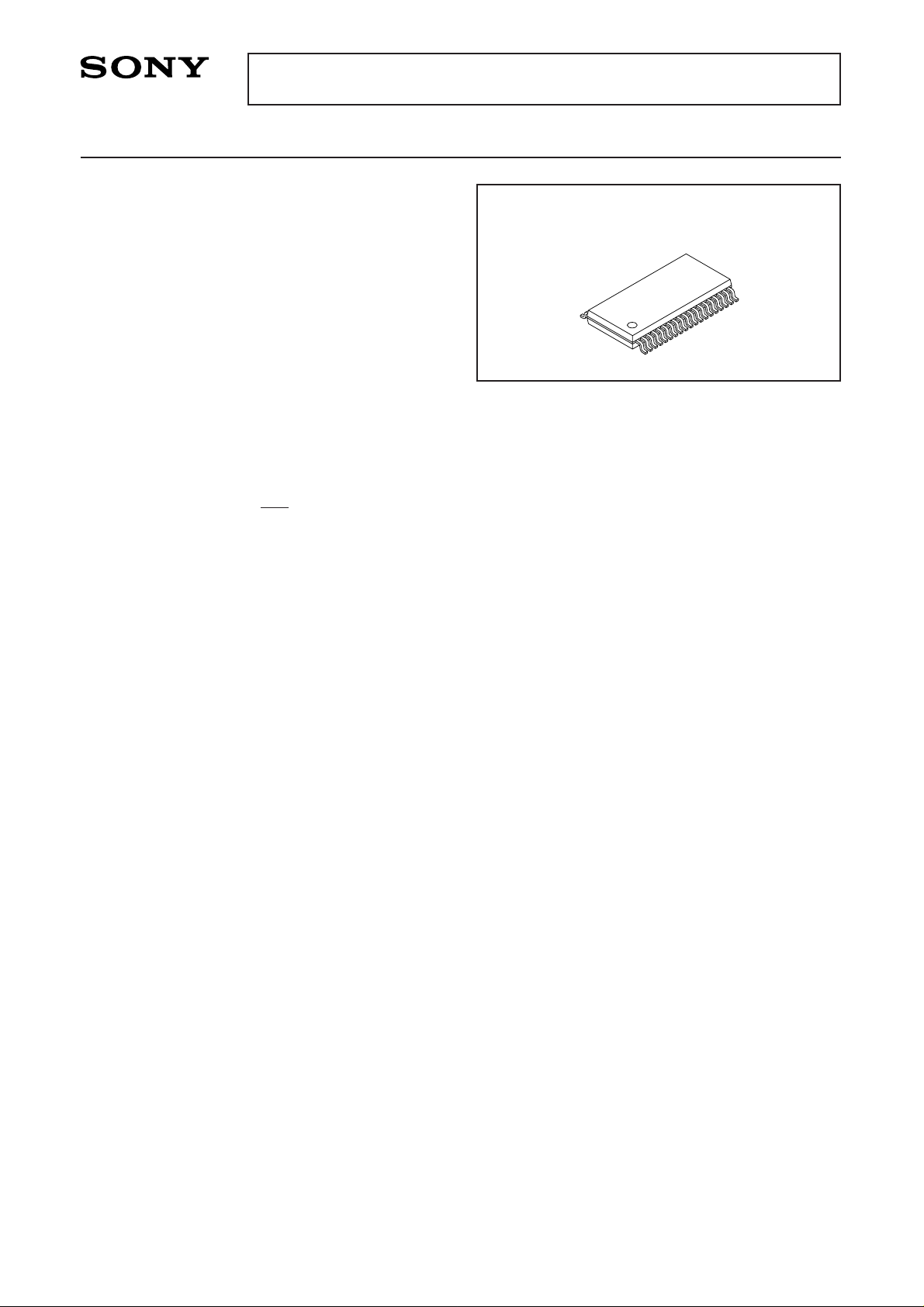
The CXA3238TN/CXA3239TN is a Read/Write
amplifier for GMR-Ind (Giant Magneto ResistiveInductive) heads used in hard disk drives, and is
capable of supporting up to six channels.
Features
• +5 V and –3 V power supply.
• Current bias voltage sense type.
• Drives up to six heads (CXA3238TN)
• Drives up to four heads (CXA3239TN)
• Low power 180 mW at Read
• Differential read amplifier gain ; ×140/190
(RMR=50 Ω)
• Input noise of 0.77 nV/ √ Hz (typ.),
RMR=50 Ω, IB=6.0 mA.
• Recovery time write to read ; 300 nsec. (typ.)
• Write data is triggered by differential P-ECL signal.
• Servo bank write. (All channels)
• Write unsafe detection circuit.
• Serial port
…
Head selection
MR bias
Write current
Applications
Hard disk drives with GMR-Ind heads.
Structure
Bipolar silicon monolithic IC
6/4-channel Read/Write Amplifier for GMR-Ind Head Hard Disk Drive
38 pin TSSOP (Plastic)
CXA3238TN/CXA3239TN
For the availability of this product, please contact the sales office.
Page 2
—2—
CXA3238TN/CXA3239TN
AMP
DRIVER
DRIVER
DRIVER
DRIVER
AMP
AMP
DRIVER
AMP
DRIVER
AMP
AMP
Bias
current
source
Write
current
source
WD BUF
Serial Interface
AMP
20
21
22
23
24
25
26
27
28
29
30
31
32
33
34
35
36
37
38
RS
SCLK
SDATA
WDX
WDY
V
CC
GND
RDY
RDX
FLT/SE/BHV
R/XW
SDEN
CAP
V
EE
W0X
W0Y
R0X
R0Y
W1X
R5Y
R5X
W5Y
W5X
W4X
W4Y
R4X
R4Y
R3Y
R3X
W3Y
W3X
W2X
W2Y
R2X
R2Y
R1Y
R1X
W1Y
1
2
3
4
5
6
7
8
9
10
11
12
13
14
15
16
17
18
19
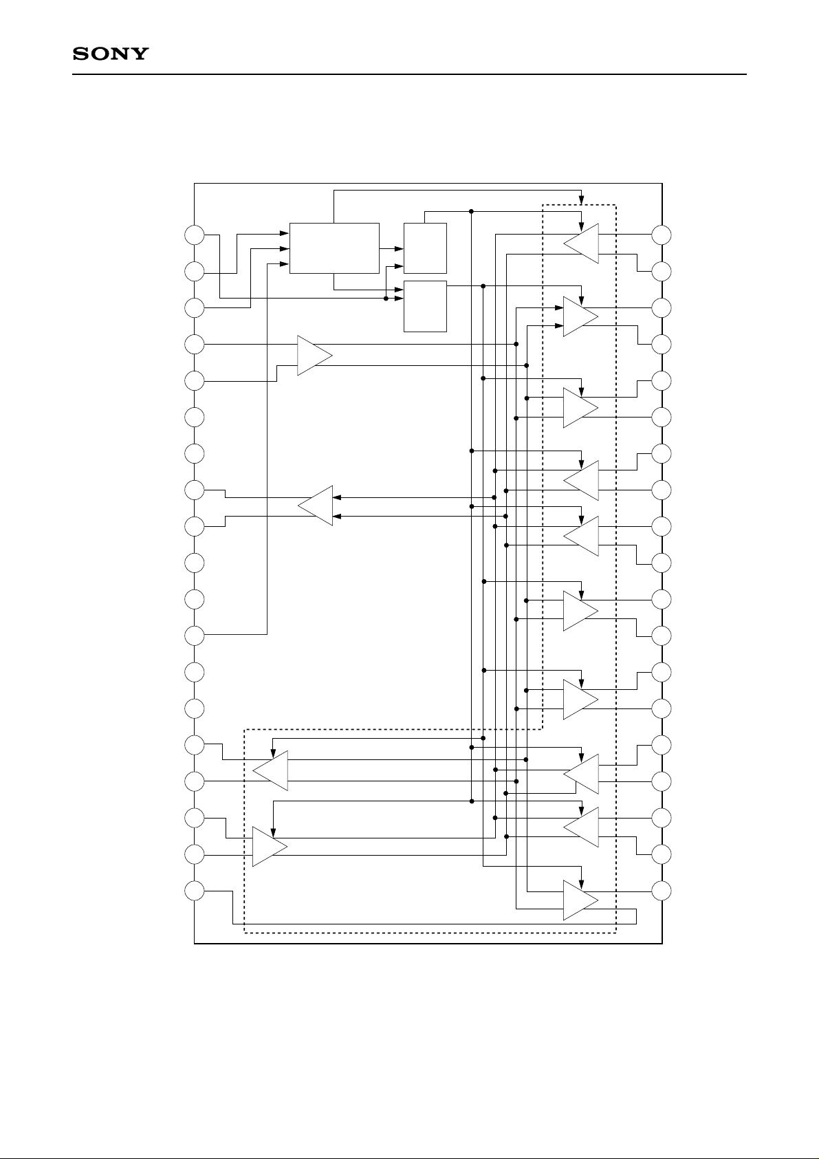
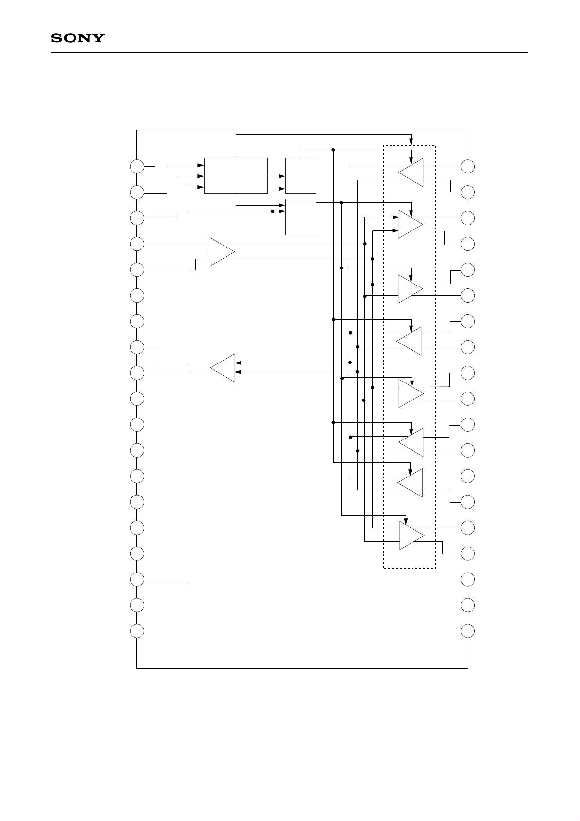
Block Diagram and Pin Configuration
CXA3238TN
Page 3
—3—
CXA3238TN/CXA3239TN
CXA3239TN
AMP
DRIVER
DRIVER
AMP
Bias
current
source
Write
current
source
WD BUF
Serial Interface
20
21
22
23
24
25
26
27
28
29
30
31
32
33
34
35
36
37
38
AMP
RS
SCLK
SDATA
WDX
WDY
VCC
GND
RDY
RDX
FLT/SE/BHV
NC
NC
NC
NC
NC
R/XW
SDEN
CAP
VEE
R3Y
R3X
W3Y
W3X
W2X
W2Y
R2X
R2Y
W1X
W1Y
R1X
R1Y
R0Y
R0X
W0Y
W0X
NC
NC
VEE
1
2
3
4
5
6
7
8
9
10
11
12
13
14
15
16
17
18
19
AMP
DRIVER
AMP
DRIVER
Page 4
—4—
CXA3238TN/CXA3239TN
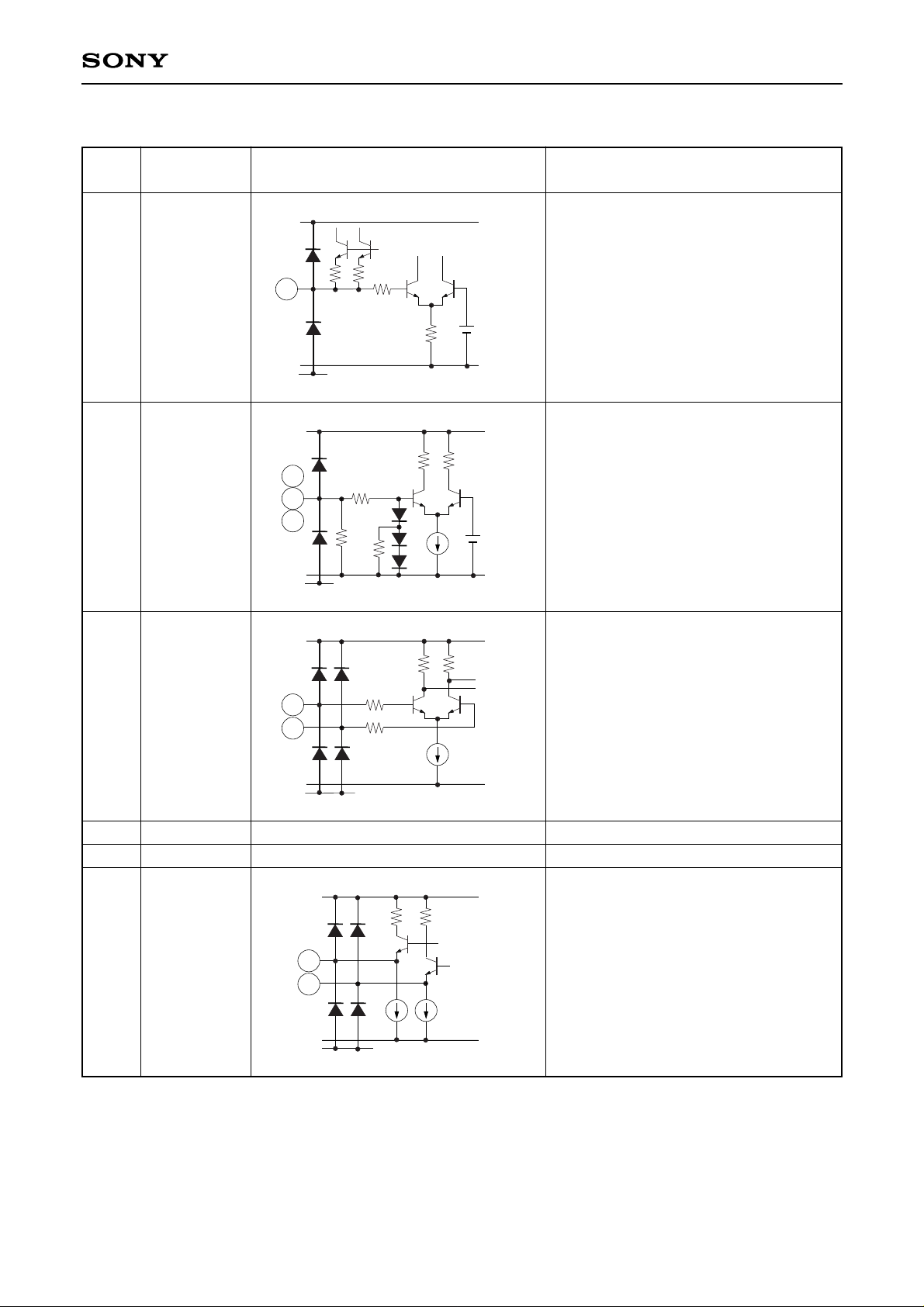
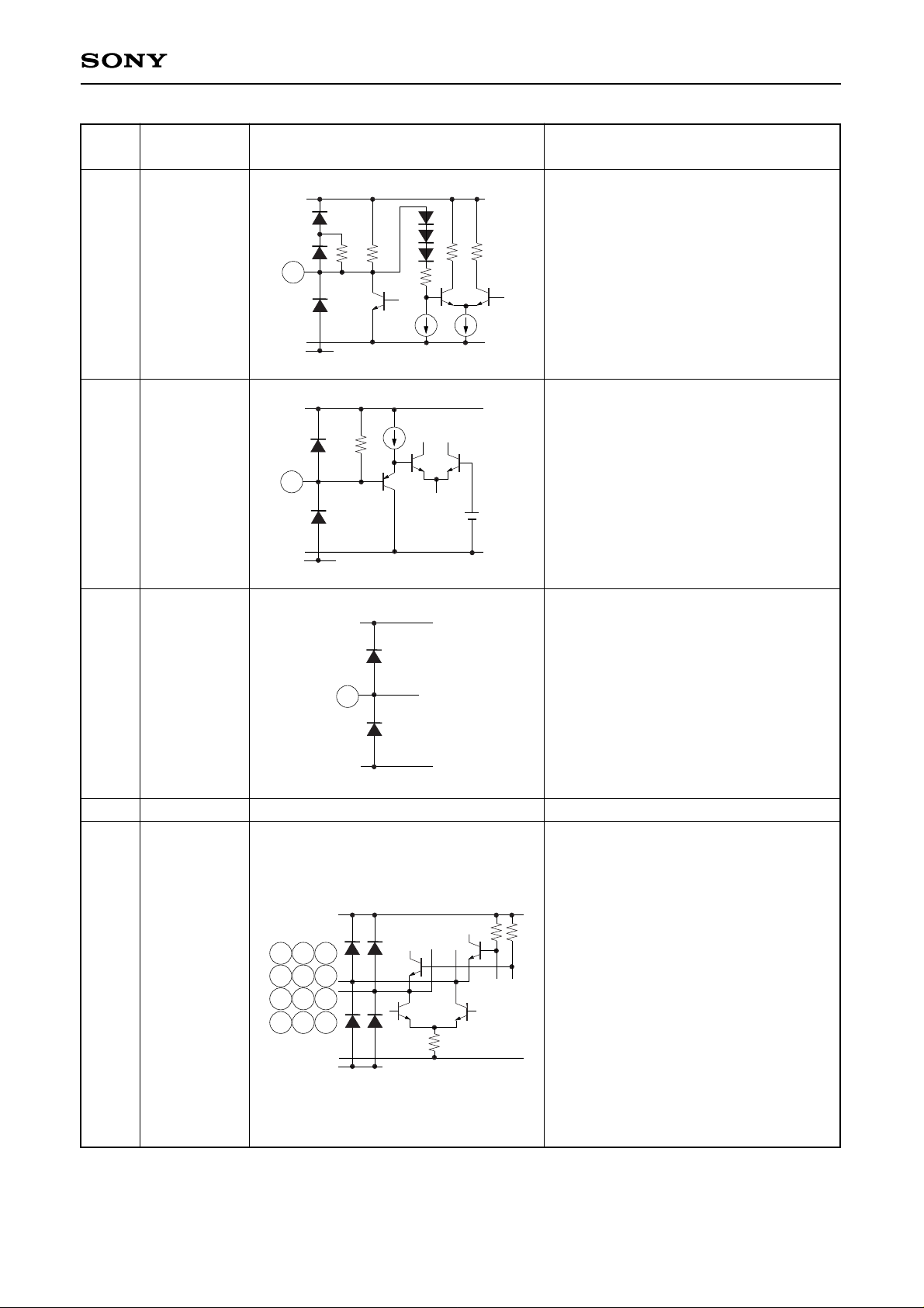
Pin Description CXA3238TN
Pin
Symbol Equivalent circuit Description
No.
1
2
3
12
4
5
6
7
9
8
RS
SCLK
SDATA
SDEN
WDX
WDY
VCC
GND
RDX
RDY
VCC
VEE
GND
250
VBGR
≈1.3V
1
VCC
VEE
GND
2
3
12
14k
7.5k
2Vf
VCC
VEE
GND
100
100
4
5
VCC
VEE
GND
8
9
100
1.8mA
Bias current setting resister is connected
between this pin and GND.
Serial control signal input.
Differential P-ECL write data input.
5 V power supply.
Ground
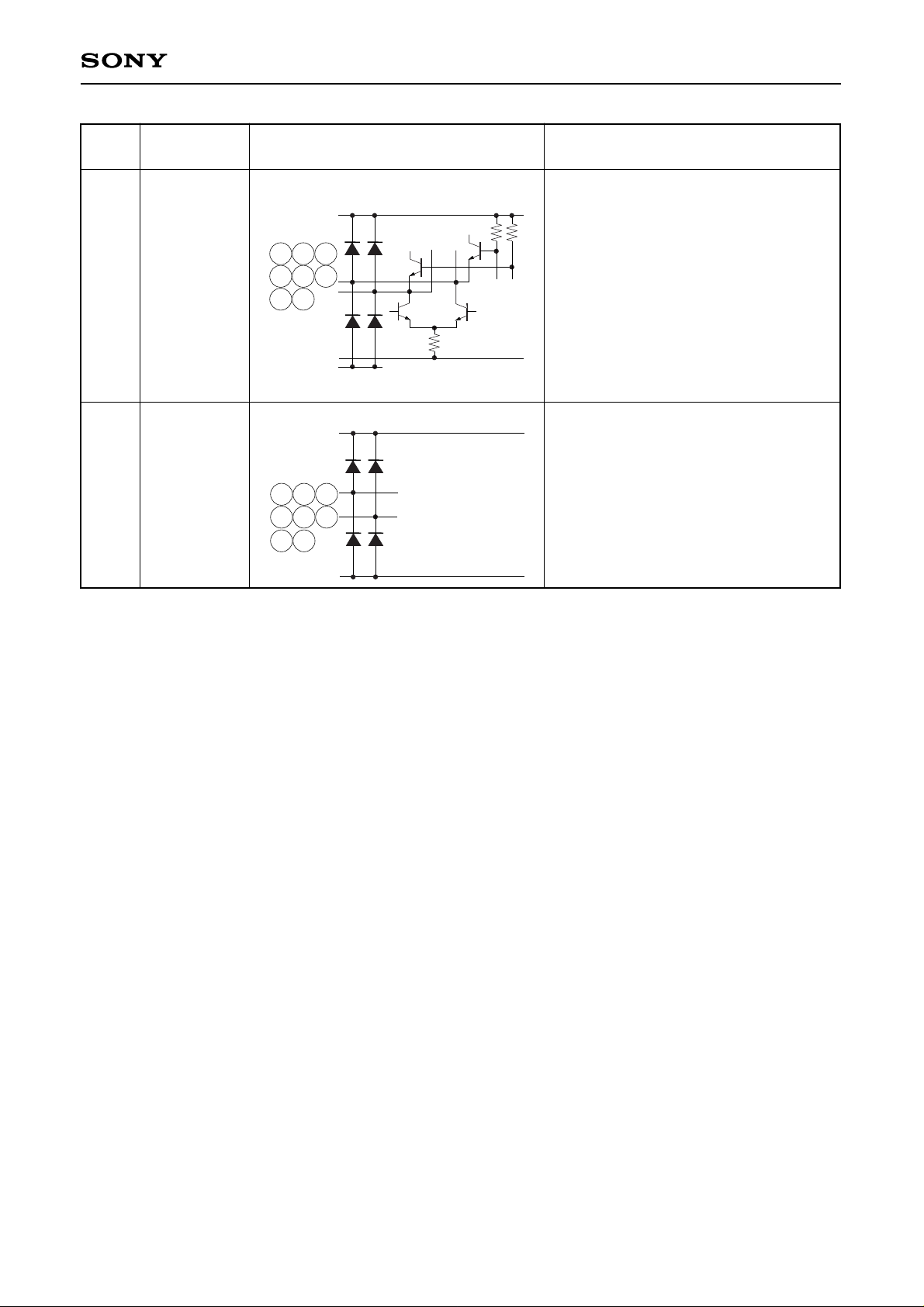
Read amplifier output with coupling
capacitors.
High impedance in the write mode.
Page 5
—5—
CXA3238TN/CXA3239TN
Pin
Symbol Equivalent circuit Description
No.
10
11
13
14
15
16
19
20
26
25
27
28
34
33
35
36
FLT/SE/BHV
R/XW
CAP
VEE
W0X
W0Y
W1X
W1Y
W2X
W2Y
W3X
W3Y
W4X
W4Y
W5X
W5Y
VCC
VEE
GND
100 10k
10
VCC
VEE
GND
100k
3Vf
11
VCC
VEE
13
VCC
VEE
GND
151619
20 25
26
27
28 33
34 35
36
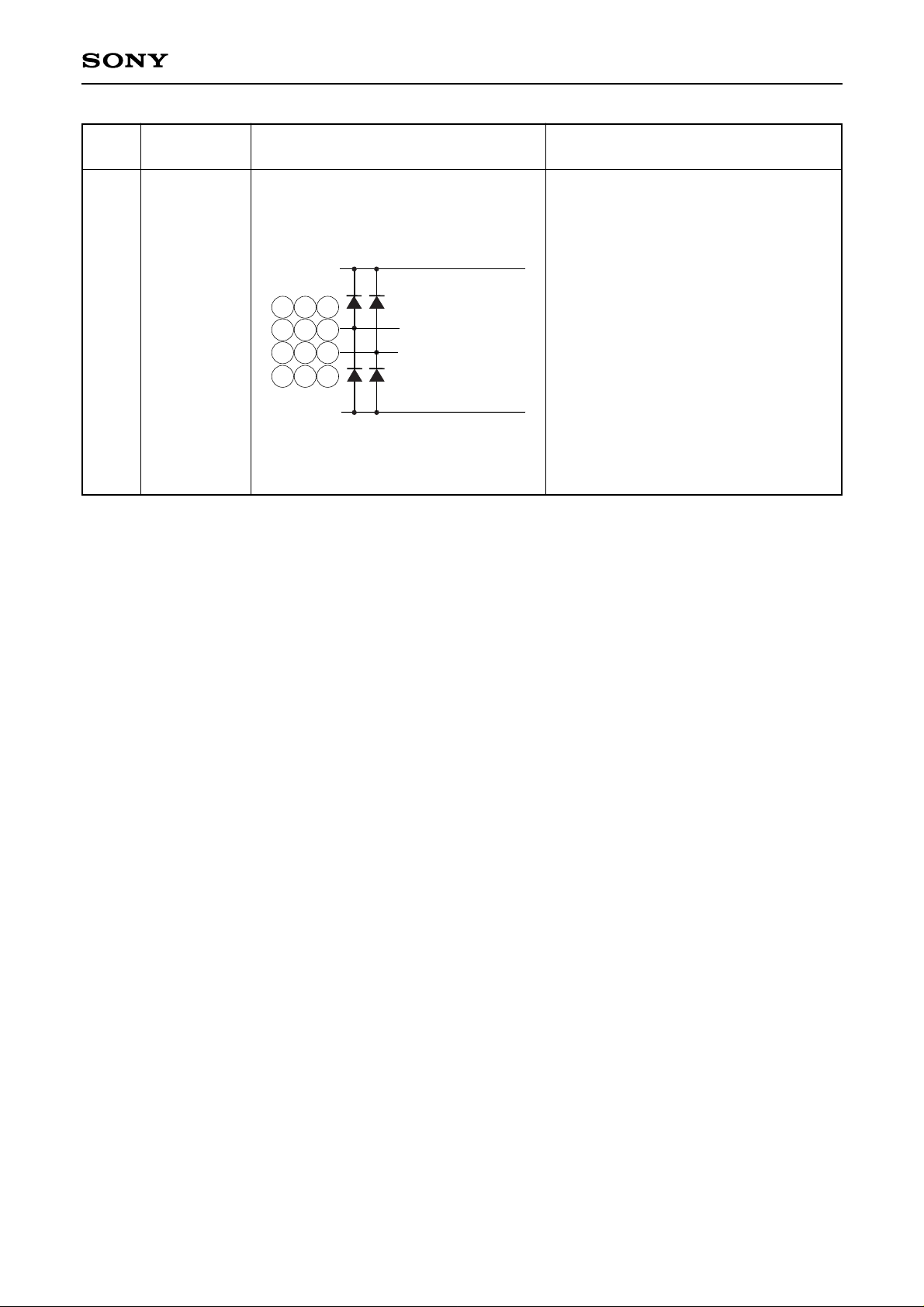
Head unsafe detection output.
Servo Bank Write Enable input.
Buffered Head Voltage output.
Read / Write control signal input.
Read when high, Write when low.
Connect an external capacitor of Read
amplifier between this pin and VEE.
–3 V power supply.
Inductive heads for Write.
Six channels are provided.
Page 6
—6—
CXA3238TN/CXA3239TN
Pin
Symbol Equivalent circuit Description
No.
17
18
21
22
24
23
29
30
32
31
37
38
R0X
R0Y
R1X
R1Y
R2X
R2Y
R3X
R3Y
R4X
R4Y
R5X
R5Y
VCC
VEE
171821
22 23
24
29
30 31
32 37
38
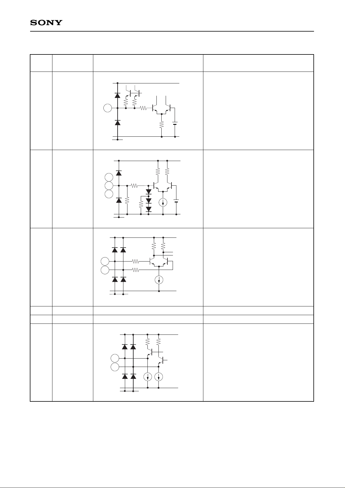
MR heads for Read.
Six channels are provided.
Page 7
—7—
CXA3238TN/CXA3239TN
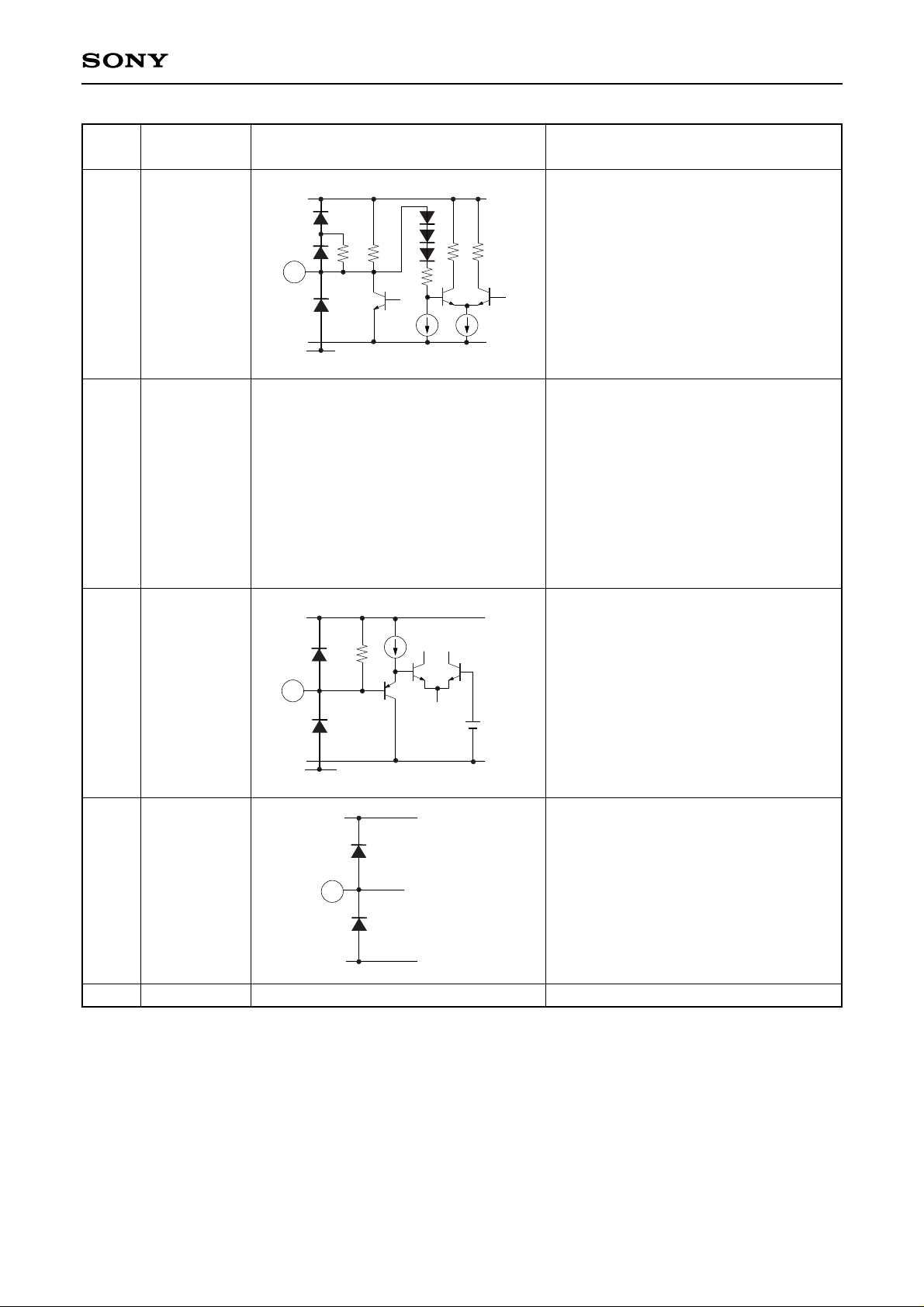
Pin Description CXA3239TN
Pin
Symbol Equivalent circuit Description
No.
1
2
3
17
4
5
6
7
9
8
RS
SCLK
SDATA
SDEN
WDX
WDY
VCC
GND
RDX
RDY
VCC
VEE
GND
250
VBGR
≈1.3V
1
VCC
VEE
GND
2
3
17
14k
7.5k
2Vf
VCC
VEE
GND
100
100
4
5
VCC
VEE
GND
8
9
100
1.8mA
Bias current setting resister is connected
between this pin and GND.
Serial control signal input.
Differential P-ECL write data input.
5 V power supply.
Ground
Read amplifier output with coupling
capacitors.
High impedance in the write mode.
Page 8
—8—
CXA3238TN/CXA3239TN
—8—
Pin
Symbol Equivalent circuit Description
No.
10
11
12
13
14
15
21
22
16
18
19, 20
FLT/SE/BHV
NC
R/XW
CAP
VEE
VCC
VEE
GND
100 10k
10
VCC
VEE
GND
100k
3Vf
16
VCC
VEE
18
Head unsafe detection output.
Servo Bank Write Enable input.
Buffered Head Voltage output.
Non Connection
Read / Write control signal input.
Read when high, Write when low.
Connect an external capacitor of Read
amplifier between this pin and VEE.
–3 V power supply.
Page 9
—9—
CXA3238TN/CXA3239TN
Pin
Symbol Equivalent circuit Description
No.
23
24
29
30
33
34
35
36
25
26
27
28
31
32
37
38
W0X
W0Y
W1Y
W1X
W2Y
W2X
W3X
W3Y
R0X
R0Y
R1Y
R1X
R2Y
R2X
R3X
R3Y
VCC
VEE
GND
2335243629
30 33 34
Inductive heads for Write.
Four channels are provided.
MR heads for Read.
Four channels are provided.
VCC
VEE
28 31 32
25
37 38
26 27
Page 10

—10—
CXA3238TN/CXA3239TN
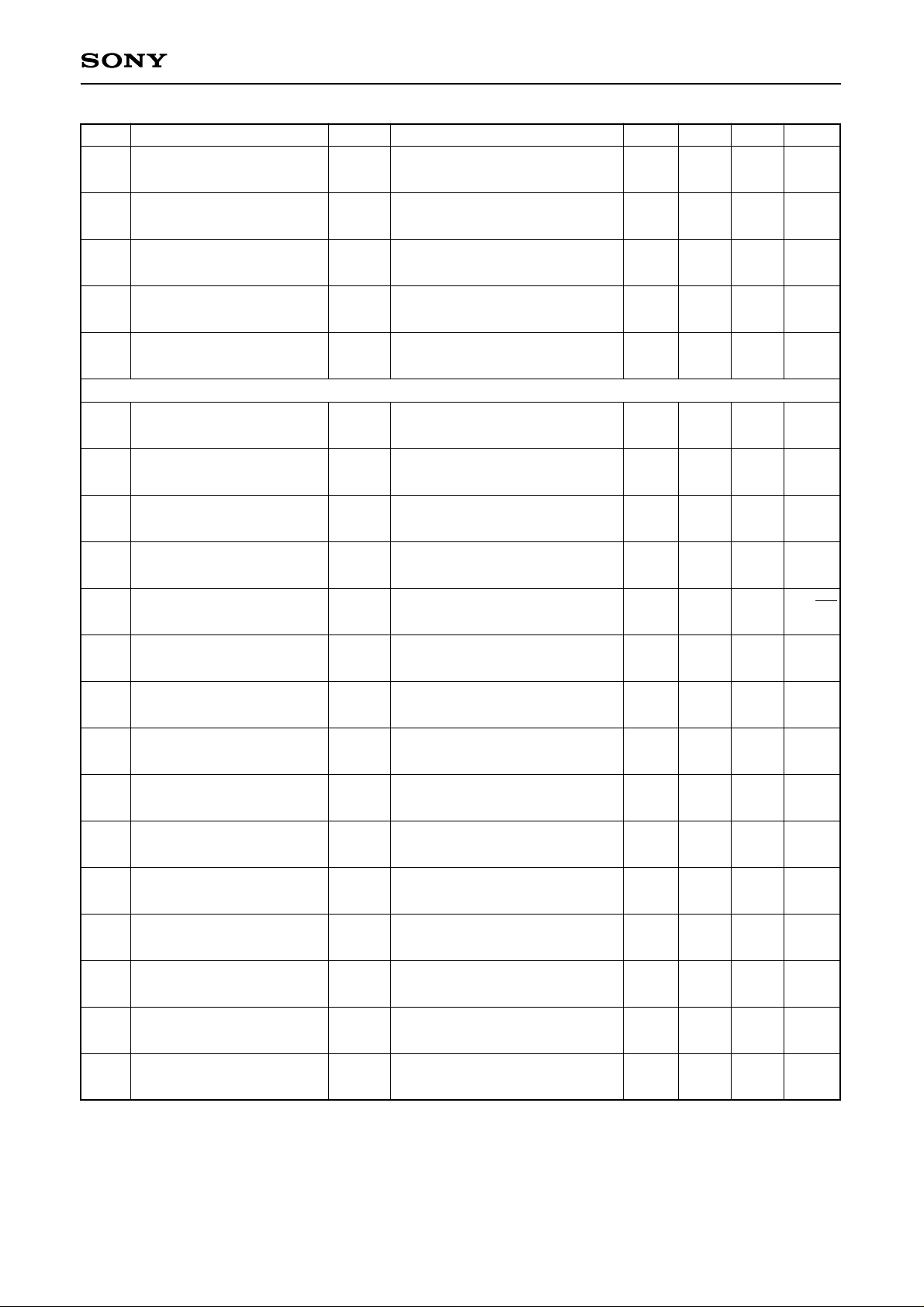
Electrical Characteristics
(Unless otherwise specified; VCC=5 V, VEE=–3 V, Ta=25 °C, CAP=0.1 µF, RS=7.5 kΩ)
No. Item Symbol Measurement conditions Min. Typ. Max. Unit
Power Dissipation IW=31 mA, IB=6.0 mA
Digital Inputs
1-1
1-2
1-3
1-4
1-6
1-7
1-8
1-9
VCC power supply current
VEE power supply current
Bank write mode
ISP1
IID1
IRE1
IWR1
IID2
IRE2
IWR2
ICCBW
VIL
VIH
ITTL
VSIL
VSIH
IST
VWDV
VWDA
IWD
VPIH
VPIL
Vdiff
SLEEP mode
IDLE mode
Read mode
Write mode
IDLE mode
Read mode
Write mode
ICCBW=17+17×N+IW×N,
IW=31 mA
TTL input; R/XW
Pull-up resister : 100 kΩ
High voltage : 5 V
Low voltage : 0 V
Serial input; SDATA, SCLK,
SDEN
High voltage : 5 V, Low voltage : 0 V
Pull-down resister : 14 kΩ
Write data input
Input voltage : 4 V
VDD=3.3 V
(VPIH–VPIL) × 2
2.1 2.8 mA
22 29 mA
36 47 mA
80 100 mA
10 13 mA
10 13 mA
10 13 mA
300 mA
0 0.8 V
2.0
VCC+
V
0.3
–100 100 µA
1 V
4 V
–1000 1000 µA
VCC VCC
V
–2.5 +0.3
0.3 1.5 V
–20 20 µA
VDD–0.2
VDD V
2.0
VDD–0.5VDD–0.3
V
400 800 1300 mV
TTL input
low input voltage
TTL input
high input voltage
TTL input
input current
Serial interface input
low input voltage
Serial interface input
high input voltage
Serial interface input
input current
P ECL input
Voltage range
P ECL input
Input amplitude
P ECL input current
P ECL input
high input voltage 2
P ECL input
low input voltage 2
P ECL input
differential voltage 2
2-1
2-2
2-3
2-4
2-5
2-6
3-1
3-2
3-3
3-4
3-5
3-6
Page 11
—11—
CXA3238TN/CXA3239TN
No. Item Symbol Measurement conditions Min. Typ. Max. Unit
4-1
4-2
5-1
5-2
6
Bank Write Enable
voltage
Bank Write Enable
current
FLT output low voltage
FLT output high voltage
BHV gain accuracy
VSEH
ISEH
VFLTL
VFLTH
EBHV
External resistance=2.4 kΩ
External resistance=2.4 kΩ
VBHV=VCC–4×IB×(RMR+5.5 Ω)
IB=“1,1,1” RMR=50 Ω
VCC VCC
V
+1.2 +1.4
6 14 mA
0.8 V
4.5 V
–8 8 %
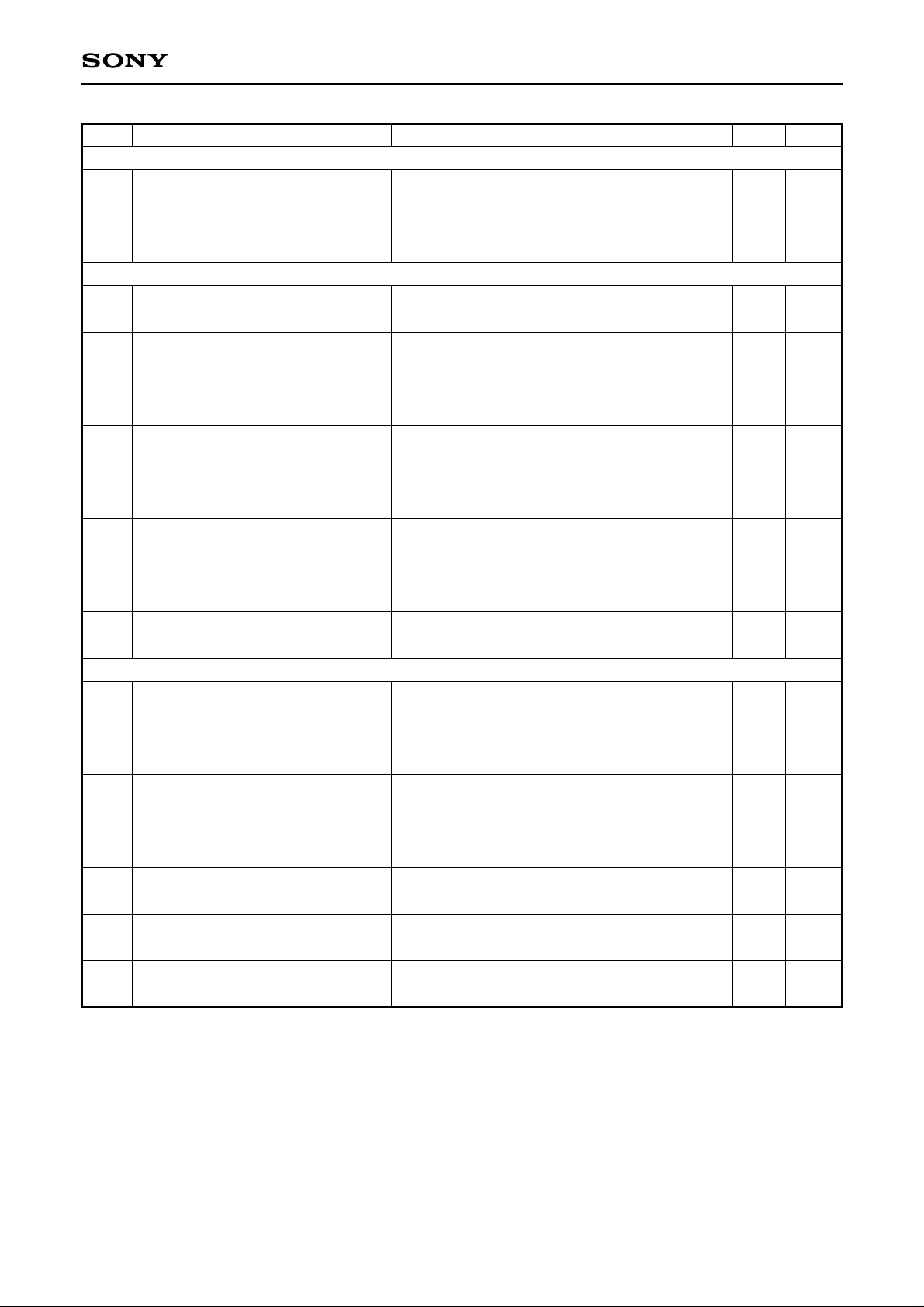
Read Characteristics RMR=50 Ω, IB=6.0 mA
AVL
AVH
FCL
FCH
ENI
IBR1
EIB
RIB
PSRR1
PSRR2
CMRR1
CMRR2
CLRR
VOFF1
RDro
[GAIN]=0
RMR=50 Ω, IB=6.0 mA
[GAIN]=1
RMR=50 Ω, IB=6.0 mA
Exclusive of Head noise
RMR=50 Ω, IB=6.0 mA
3 bit DAC
Ripple voltage : 100 mVp-p
100 kHz to 50 MHz
Ripple voltage : 100 mVp-p
100 kHz to 10 MHz
Ripple voltage : 100 mVp-p
100 kHz to 50 MHz
Ripple voltage : 100 mVp-p
51 MHz to 80 MHz
Ripple voltage : 100 mVp-p
4 MHz to 80 MHz
Write to Read
Differential, read mode
115 140 165 V/V
155 190 225 V/V
350 550 kHz
140 200 MHz
0.77 0.95
nV/ √ Hz
3 8 mA
–7 +7 %
0.714 mA
38 dB
45 dB
37 dB
27 dB
40 dB
50 mV
30 100 Ω
Low Gain
High Gain
Low frequency cut-off
(–3 dB)
High frequency cut-off
(–3 dB)
Input reflected noise
MR bias current range 1
MR bias accuracy
MR bias resolution
VCC power supply
rejection ratio
VEE power supply
rejection ratio
Common mode
rejection ratio 1
Common mode
rejection ratio 2
Control line input noise
rejection
RDX/RDY offset difference
magnitude
RDX/RDY output
impedance
R1
R2
R3
R4
R5
R6
R7
R8
R9-1
R9-2
R10-1
R10-2
R11
R12
R13
Page 12
—12—
CXA3238TN/CXA3239TN
No. Item Symbol Measurement conditions Min. Typ. Max. Unit
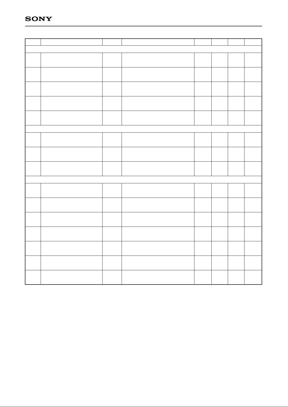
Read Safety Characteristics
Write Characteristics
P1
P2
W1
W2
W3
W4
W6
W7
W8
W9
MR head open threshold
MR head short threshold
Write current range
Write current accuracy
Write current resolution
Leakage current
Damping register
Write current propagation
delay time
Write current rise/fall time
Erase current accuracy
MRop
MRsh
IWR
EIW
RIW
ILEAK
RD
Tpd
TR/TF
EIE
Head X - Head Y
Head X - Head Y
IB= ‘000’ to ‘011’
DAC code=× ‘0000’ to × ‘1111’
RH=0 Ω
4 bit DAC
Unselected head
LH=0, RH=0
Write DATA to 50 % of Write current
RH=15 Ω, LH=150 nH, IW=31 mA
VCC=3.5 V
DAC code=× ‘0101’
600 750 900 mV
15 50 90 mV
15 45 mA
–7 +7 %
2 mA
200 µA
320 420 520 Ω
10 ns
2.5 ns
–18 –9 0 %
Write Safety Characteristics
U1
U2
U3
U4
U5
U6
U7
Write head open threshold
Head voltage when short
to GND
WD frequency too low
Write safety detect time
Low VCC threshold
Low VCC threshold
Low VCC threshold
hysteresis
ROP
VG
fWDL
TWS
VWthL
VWthH
Vhys
Detect open head
Detect short to GND
T1 : 2 transitions on WDX/WDY
Fault detected
Fault removed
1.2 1.4 V
0.1 V
0.5 1.8 MHz
300
ns
+T1
3.7 3.9 4.1 V
3.9 4.1 4.3 V
200 mV
Page 13
—13—
CXA3238TN/CXA3239TN
No. Item Symbol Measurement conditions Min. Typ. Max. Unit
Switching Characteristics IW=31 mA, IB=6 mA
Bank Write Characteristics IW=31 mA, IB=6 mA
S1
S2
S3
S4-1
S4-2
S5
S6
S7
B1
B2
B4
B5
B6
B7
B8
Write to Read
Read to Write
Idle to Read
Sleep to Read(A3238)
Sleep to Read(A3239)
Read to Bank Write
Bank Write to Read
Idle to Bank Write
Idle to Write
Set up time
Hold time
SCLK frequency
SCLK pulse width
SCLK-SDATA
set up time
SCLK-SDATA
hold time
SDEN low time
TWR
TRW
TIR
TSR1
TSR2
TRB
TBR
TIW
Tsu
(sden)
Th
(sden)
f (sclk)
Tw
(sclk)
Tsu (d)
Th (d)
TSL
Signal on WDX/WDY
90 % RD signal or 10 % IW
90 % I
W
90 % RD signal
90 % RD signal ,90 % IB
(*1)
IB="0,1,1"
90 % RD signal ,90 % IB
(*1)
IB="0,1,1"
90 % IW
10 % IW
90 % IW
SDEN to first SCLK
Last SCLK to deassert SDEN
300 500 ns
50 70 ns
1.0 µs
600 1000 µs
600 2000 µs
100 ns
100 ns
300 us
10 ns
10 ns
30 MHz
10 ns
10 ns
10 ns
100 ns
Serial port timing
(∗1) TSR is proportional to IB and external CAP value
Page 14
—14—
CXA3238TN/CXA3239TN
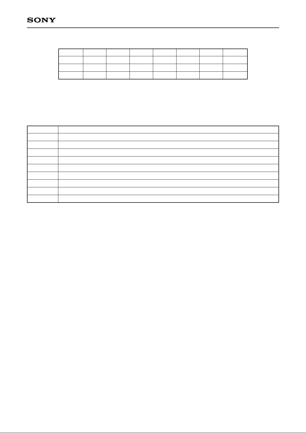
Serial port characteristics
∗IB<2-0> bits are initialized by ‘0’ at power on
ADR1 ADR0 DATA5 DATA4 DATA3 DATA2 DATA1 DATA0
0 0 XSLP XIDL N/A HS2 HS1 HS0
0 1 GAIN BHV N/A IB2 IB1 IB0
1 0 MROPN MRSHT IW3 IW2 IW1 IW0
Code Description
Bit
XSLP
XIDL
HS<2-0>
GAIN
BHV
IB<2-0>
MROPN
MRSHT
IW<3-0>
Function
“0” = Set the pre-amp into low power “sleep” mode
“0” = Set preamplifier to idle mode
Head select bit
Set the pre-amp to high or low gain mode. “1” = Set preamplifier to high gain mode
Activate the BHV test point pin. “1” active.
MR bias current set
“1” = Set MR head open detector active.
“1” = Set MR head short detector active.
Set write current
Page 15
—15—
CXA3238TN/CXA3239TN
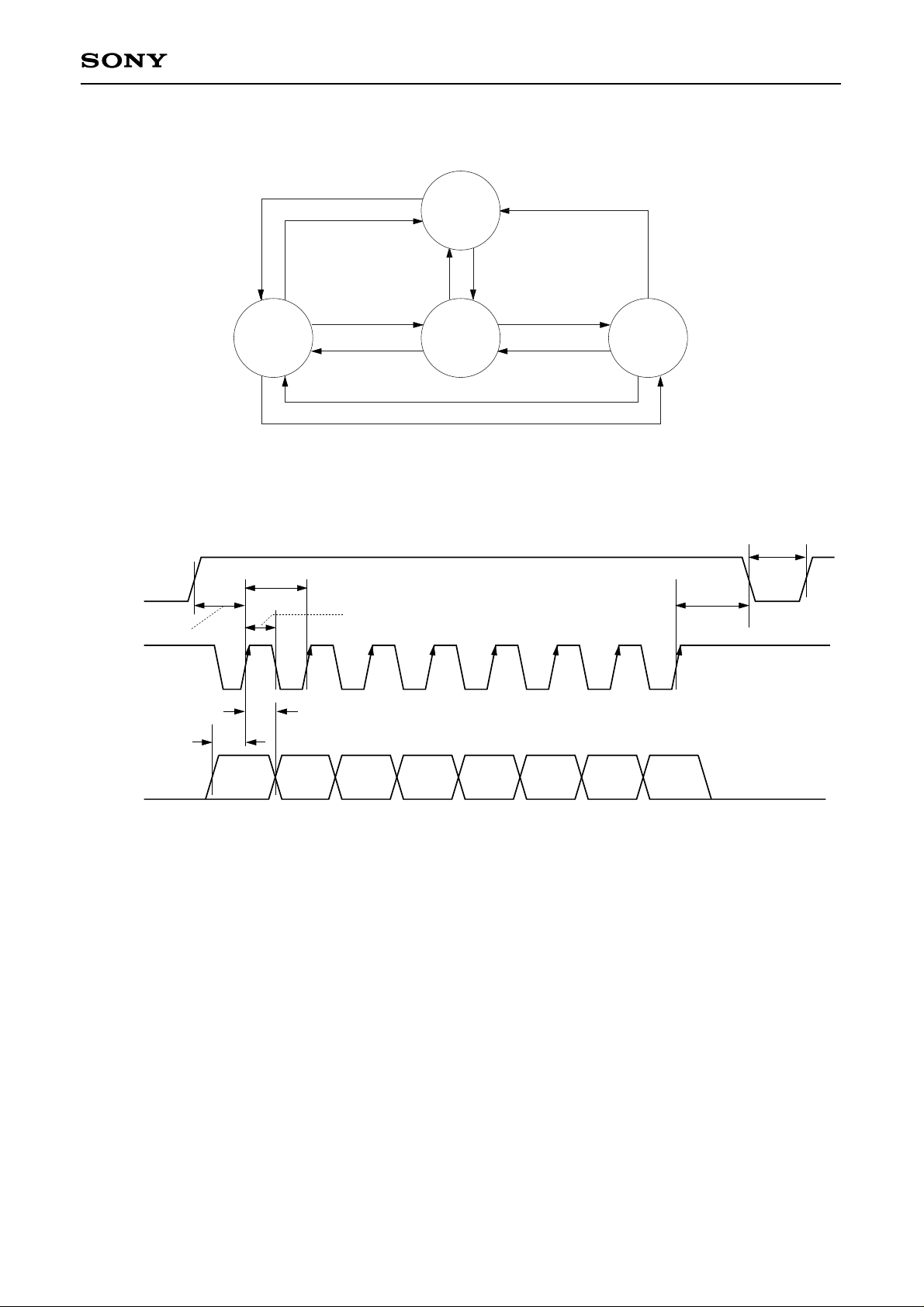
Mode Control
Serial Port Timing Detail
Serial Port Timing
After the SDEN goes high, the last eight bits are transferred into the register. The SCLK will shift the data
presented at the SDATA into an internal shift register on the rising edge of each clock.
As SCLK initial condition, both of Low and High signal is acceptable.
WRITE
XSLP=1
XIDL=1
R/XW=L
READ
XSLP=1
XIDL=1
R/XW=H
IDLE
XSLP=1
XIDL=0
R/XW=X
SLEEP
XSLP=0
TSL
Th (sden)
Tsu (sden)
Tsu (d)
Th (d)
Tw (sclk)
f (sclk)
A1 A0 D5 D4 D3 D2 D1 D0
SDEN
SCLK
SDATA
Page 16
—16—
CXA3238TN/CXA3239TN
♦ Unsafe condition
1. Write fault condition
FLT is a high level in write fault condition.
• Open write head leads. fWD < 15 MHz
• Write head leads shorted to ground.
• WD frequency is too low.
• Power supply is out of tolerance.
2. Read fault condition
FLT is a low level in read fault condition.
• Open and short MR head. (This function is set by serial register)
♦ Bank write control (refer to ‘Bank write current vs Current accuracy’ characteristic curve)
1. Set the Read mode.
2. Force a certain voltage(min.VCC+1.2V) to FLT/SE pin by using the pull-up resister(Rse=820Ω)
#This operation disables all Fault detection.
3. Set VCC at 3.5 V (in case of Erase mode only)
4. Start the write operation by setting R/XW = “L”.
5. Terminate the write operation by setting R/XW = “H”.
i) Allow 50 % write duty or less.
ii) Low voltage detector is disabled in Bank Write mode and Erase mode.
iii) Don’t change the serial register data bits in following conditions :
∗) VCC=3.5 V
∗∗) On entering Write data
♦ BHV (Buffered Head Voltage)
1. Applicable within VCC=5 V±5 %
2. Turn BHV on,but turn off MROPN and MRSHT
3. VBHV is determined by basis of VCC. VBHV =VCC–4 × IB × (RMR+5.5 Ω)
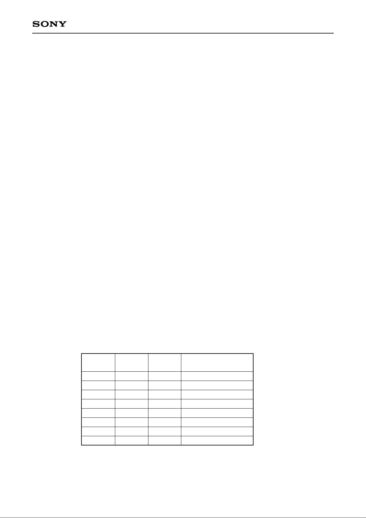
♦ Head select table
6ch
HS2
0
0
0
0
1
1
1
1
HS1
0
0
1
1
0
0
1
1
HS0
0
1
0
1
0
1
0
1
Head select,
Normal operation
0
1
2
3
4
5
none
none
Page 17
—17—
CXA3238TN/CXA3239TN
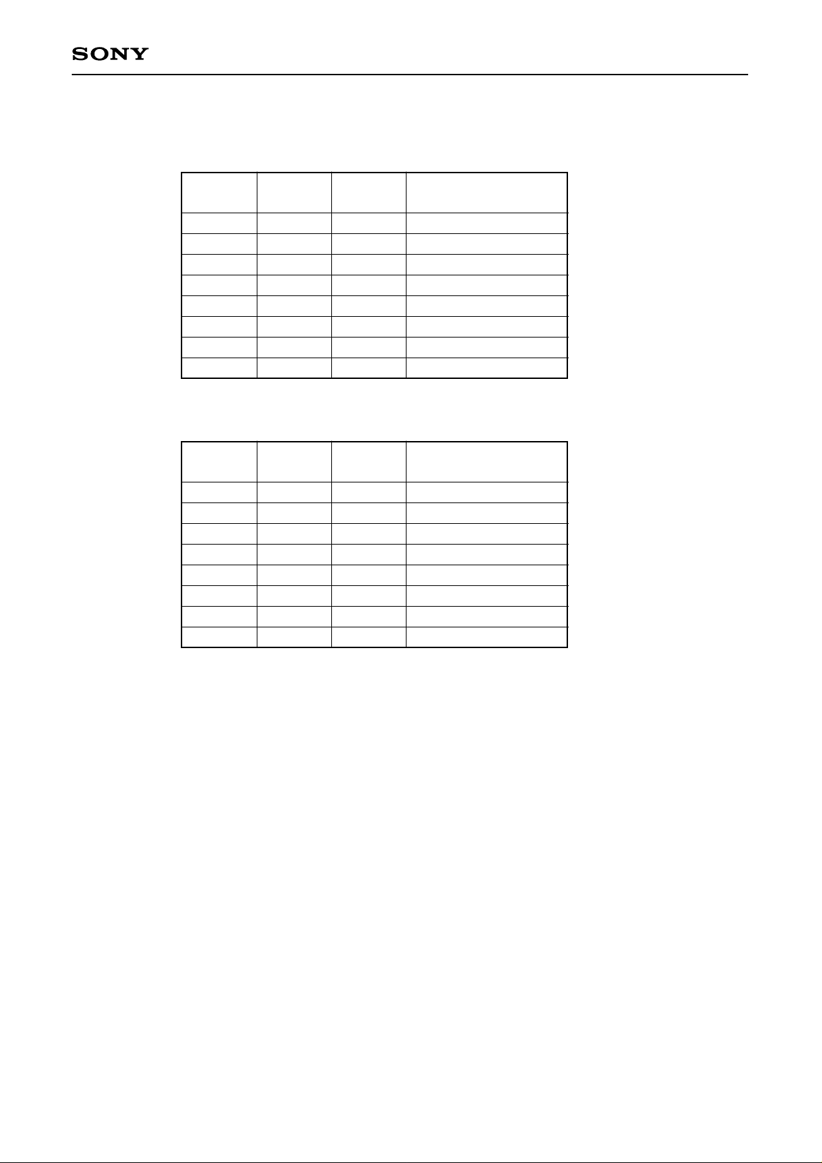
♦ Head select table
4ch
♦ MR Bias
HS2
0
0
0
0
1
1
1
1
HS1
0
0
1
1
0
0
1
1
HS0
0
1
0
1
0
1
0
1
Head select,
Normal operation
0
1
2
3
none
none
none
none
IB2
0
0
0
0
1
1
1
1
IB1
0
0
1
1
0
0
1
1
IB0
0
1
0
1
0
1
0
1
IB (mA)
3.0
3.714
4.429
5.143
5.857
6.571
7.286
8.0
Page 18
—18—
CXA3238TN/CXA3239TN
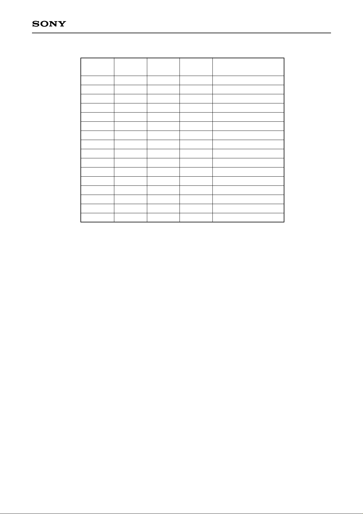
♦ Write current
IW3
0
0
0
0
0
0
0
0
1
1
1
1
1
1
1
1
IW2
0
0
0
0
1
1
1
1
0
0
0
0
1
1
1
1
IW1
0
0
1
1
0
0
1
1
0
0
1
1
0
0
1
1
IW0
0
1
0
1
0
1
0
1
0
1
0
1
0
1
0
1
Write current
(mA 0-P)
15
17
19
21
23
25
27
29
31
33
35
37
39
41
43
45
(*1) Actual head current is defined by the following equation:
Ihead=Iw/ (I+Rh/Rd)
Rh : Head Resistance
Rd : Damping Resistance
(*2) Short X-Y terminal on un-used head
Page 19
—19—
CXA3238TN/CXA3239TN
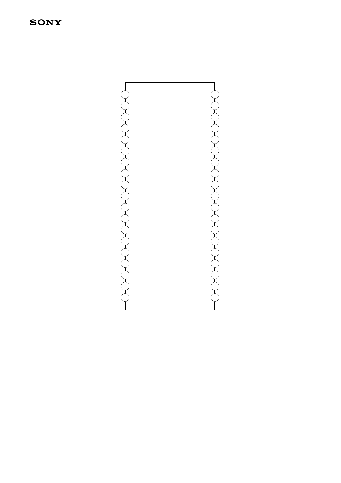
♦ 6ch CXA3238TN
1
2
3
4
5
6
7
8
9
10
11
12
13
14
15
16
17
18
19 20
21
22
23
24
25
26
27
28
29
30
31
32
33
34
35
36
37
38
RS
SCLK
SDATA
WDX
WDY
V
CC
GND
RDY
RDX
FLT/SE/BHV
R/XW
SDEN
CAP
V
EE
W0X
W0Y
R0X
R0Y
W1X
R5Y
R5X
W5Y
W5X
W4X
W4Y
R4X
R4Y
R3Y
R3X
W3Y
W3X
W2X
W2Y
R2X
R2Y
R1Y
R1X
W1Y
TSSOP 38Pin 0.5 mm pitch
Package dimension including leads 6.4 × 9.7 mm
Page 20
—20—
CXA3238TN/CXA3239TN
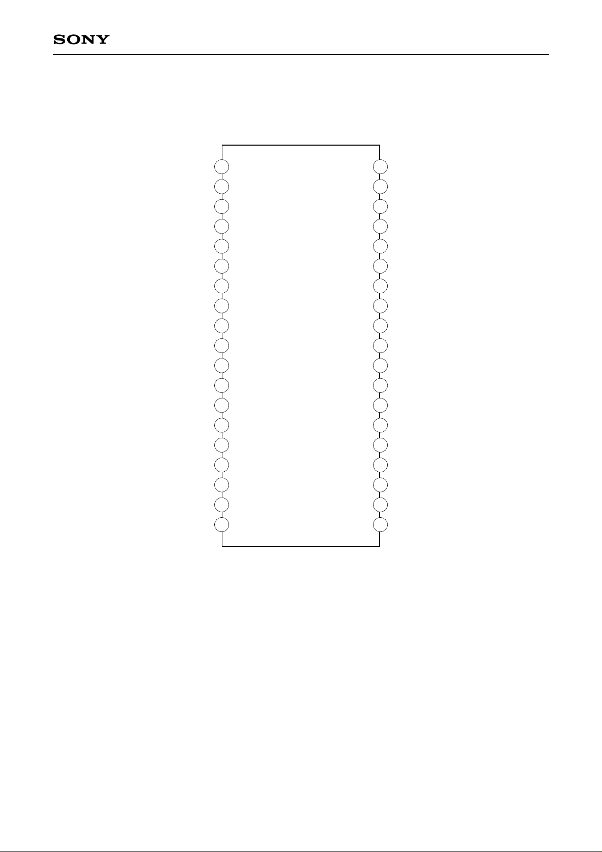
♦ 4ch CXA3239TN
1
2
3
4
5
6
7
8
9
10
11
12
13
14
15
16
17
18
19 20
21
22
23
24
25
26
27
28
29
30
31
32
33
34
35
36
37
38
RS
SCLK
SDATA
WDX
WDY
V
CC
GND
RDY
RDX
FLT/SE/BHV
NC
NC
NC
NC
NC
R/XW
SDEN
CAP
V
EE
R3Y
R3X
W3Y
W3X
W2X
W2Y
R2X
R2Y
W1X
W1Y
R1X
R1Y
R0Y
R0X
W0Y
W0X
NC
NC
V
EE
TSSOP 38Pin 0.5 mm pitch
Package dimension including leads 6.4 × 9.7 mm
Page 21

—21—
CXA3238TN/CXA3239TN
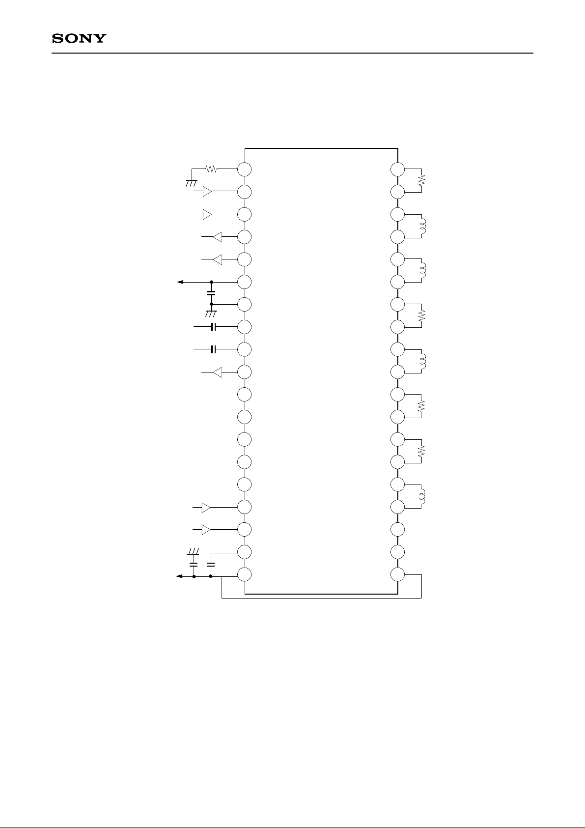
Application Circuit
CXA3238TN
RS
SCLK
SDATA
WDX
WDY
V
CC
GND
RDY
RDX
FLT/SE/BHV
R/XW
SDEN
CAP
V
EE
W0X
W0Y
R0X
R0Y
W1X
R5Y
R5X
W5Y
W5X
W4X
W4Y
R4X
R4Y
R3Y
R3X
W3Y
W3X
W2X
W2Y
R2X
R2Y
R1Y
R1X
W1Y
7.5kΩ
5V
–3V
0.1µF
0.1µF
0.1µF
1
2
3
4
5
6
7
8
9
10
11
12
13
14
15
16
17
18
19 20
21
22
23
24
25
26
27
28
29
30
31
32
33
34
35
36
37
38
Page 22
—22—
CXA3238TN/CXA3239TN
CXA3239TN
RS
SCLK
SDATA
WDX
WDY
V
CC
GND
RDY
RDX
FLT/SE/BHV
NC
NC
NC
NC
NC
R/XW
SDEN
CAP
V
EE
R3Y
R3X
W3Y
W3X
W2X
W2Y
R2X
R2Y
W1X
W1Y
R1X
R1Y
R0Y
R0X
W0Y
W0X
NC
NC
V
EE
7.5kΩ
5V
0.1µF
1
2
3
4
5
6
7
8
9
10
11
12
13
14
15
16
17
18
19 20
21
22
23
24
25
26
27
28
29
30
31
32
33
34
35
36
37
38
–3V
0.1µF
0.1µF
Page 23
—23—
CXA3238TN/CXA3239TN
RS
SCLK
SDATA
WDX
WDY
V
CC
GND
RDY
RDX
FLT/SE/BHV
R/XW
SDEN
CAP
V
EE
W0X
W0Y
R0X
R0Y
W1X
R5Y
R5X
W5Y
W5X
W4X
W4Y
R4X
R4Y
R3Y
R3X
W3Y
W3X
W2X
W2Y
R2X
R2Y
R1Y
R1X
W1Y
7.5kΩ
1kΩ
0.1µF
1µF
0.1µF
10µF
S6’
0.1µF
1µF
VPSRR’
CXA3238TN
V WDX
V WDY
V R/XW
1000pF
VCC
2.4k
S7’
180nH
25Ω
25Ω
25Ω
25Ω
25Ω
25Ω
25Ω
25Ω
25Ω
25Ω
25Ω
25Ω
VEE
3300µH
S/I
V
VSE
S6
10µF
S7
R14
1k
R13
1k
Amp2 Gain=×100
Amp1 Gain=×1
V
VM1
V
VM2
BPF
100kHz
to 50MHz
3300µH
V1
VCC
VPSRR
180nH
180nH
180nH
180nH
180nH
1
2
3
4
5
6
7
8
9
10
11
12
13
14
15
16
17
18
19 20
21
22
23
24
25
26
27
28
29
30
31
32
33
34
35
36
37
38
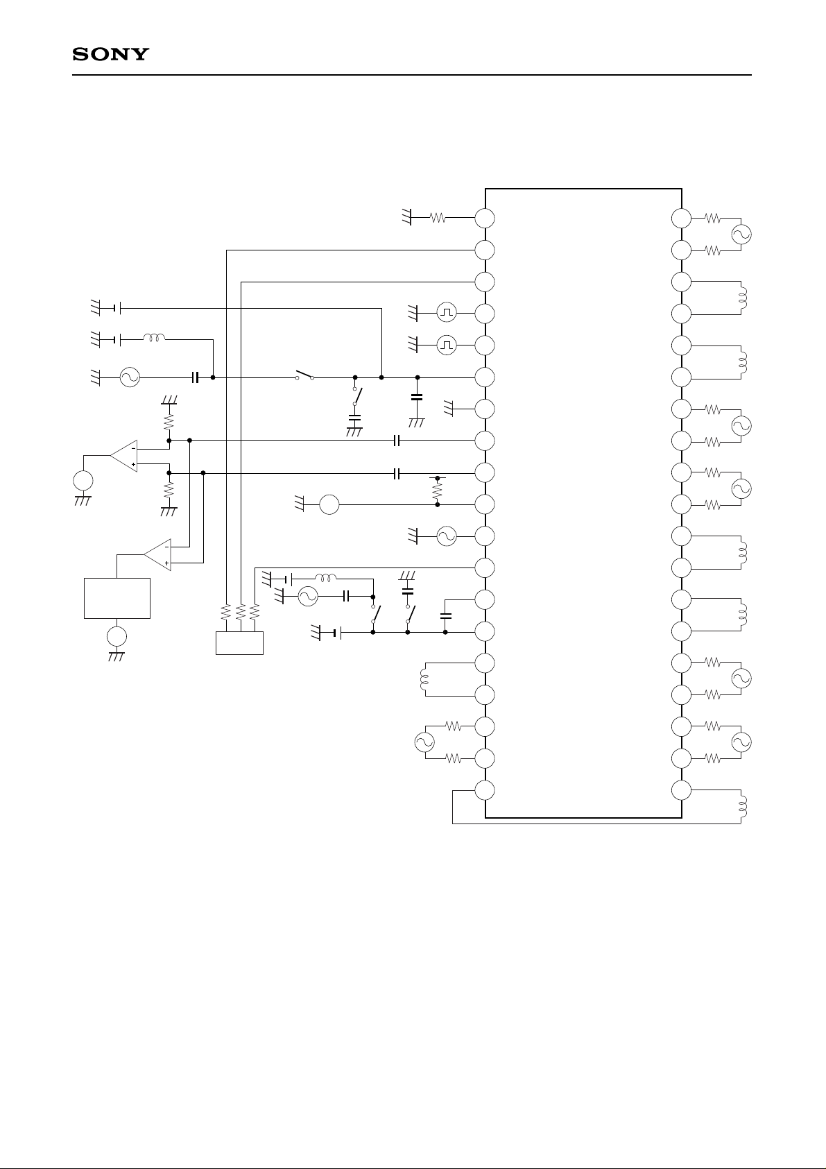
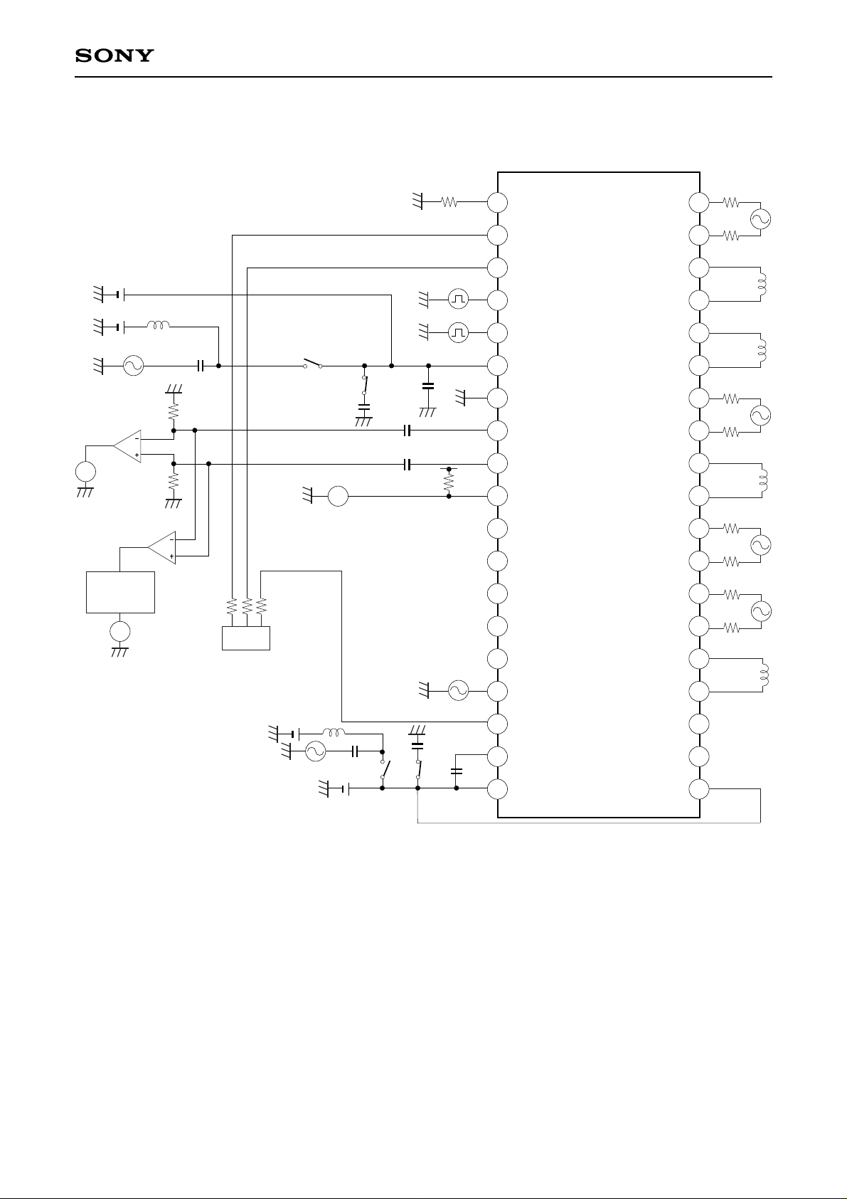
Measurement Spec.Circuit
Page 24
—24—
CXA3238TN/CXA3239TN
RS
SCLK
SDATA
WDX
WDY
V
CC
GND
RDY
RDX
FLT/SE/BHV
NC
NC
NC
NC
NC
R/XW
SDEN
CAP
V
EE
R3Y
R3X
W3Y
W3X
W2X
W2Y
R2X
R2Y
W1X
W1Y
R1X
R1Y
R0Y
R0X
W0Y
W0X
NC
NC
V
EE
7.5kΩ
1kΩ
0.1µF
1µF
0.1µF
CXA3239TN
V WDX
V WDY
1000pF
VCC
2.4k
V R/XW
25Ω
25Ω
25Ω
25Ω
25Ω
25Ω
S/I
V
VSE
S6
10µF
S7
R14
1k
R13
1k
Amp2 Gain=×100
Amp1 Gain=×1
V
VM1
V
VM2
BPF
100kHz
to 50MHz
3300µH
V1
VCC
VPSRR
180nH
180nH
180nH
20
21
22
23
24
25
26
27
28
29
30
31
32
33
34
35
36
37
38
180nH
25Ω
25Ω
10µF
S6’
0.1µF
1µF
VPSRR’
S7’
VEE
3300µH
1
2
3
4
5
6
7
8
9
10
11
12
13
14
15
16
17
18
19
Page 25
—25—
CXA3238TN/CXA3239TN
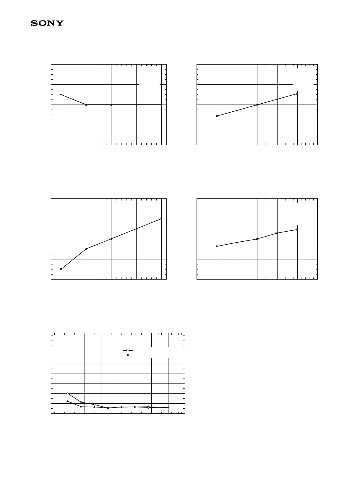
Normalized bias current vs Ambient temperature
1.04
1.02
1
0.98
0.96
–25.0 0.0 25.0 50.0 75.0
IB/IB (Ta=25°C)
Normalized bias current vs Power supply voltage
1.04
1.02
1
0.98
0.96
3.5 4 4.5 5 5.5 6.56
IB/IB (VCC=5V)
Ambient temperature Ta (°C) VCC (V)
VCC=5V
VEE=–3V
RMR=50Ω
IBn=“100”
Low gain
VEE=–3V
RMR=50Ω
IBn=“100”
Low gain
Ta=25°C
Normalized read amplifier voltage gain
vs Ambient temperature
1.04
1.02
1
0.98
0.96
–25.0 0.0 25.0 50.0 75.0
AV/AV (Ta=25°C)
Normalized read amplifier voltage gain
vs Power supply voltage
1.04
1.02
1
0.98
0.96
3.5 4 4.5 5 5.5 6.56
AV/AV (VCC=5V)
Ambient temperature Ta (°C) VCC (V)
VCC=5V
VEE=–3V
RMR=50Ω
IBn=“100”
Low gain
VEE=–3V
RMR=50Ω
IBn=“100”
Low gain
Ta=25°C
Bank write current vs Current accuracy
8
–8
6
–6
4
–4
2
–2
0
10 15 20 25 30 35 40 45 50
Bank write current accuracy (%)
Bank write current (mA)
Bank Write (A3238)
Bank Write (A3239)
VCC=5V
Ta=25°C
RH=0Ω
Read 170µs
Write 30µs
Deviation of Bank write current is within ±7% at basis of
the chart
Page 26
—26—
CXA3238TN/CXA3239TN
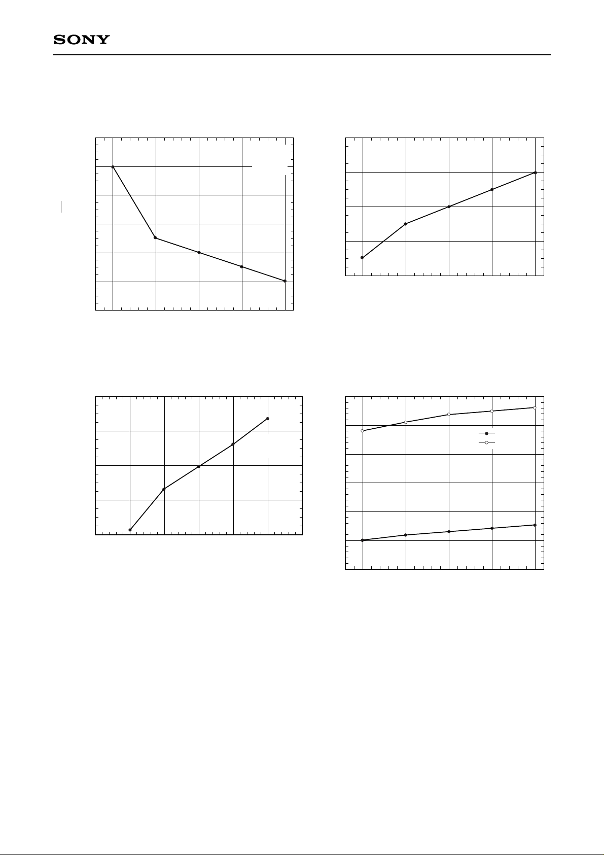
Normalized write current vs Ambient temperature
1.04
1.02
1
0.98
0.96
–25.0 0.0 25.0 50.0 75.0
IW/IW (Ta=25°C)
Ambient temperature Ta (°C)
VCC=5V
VEE=–3V
IWn=“1000”
Input refered noise voltage vs Ambient temperature
0.82
0.8
0.78
0.76
0.74
0.72
0.7
–25.0 0.0 25.0 50.0 75.0
EN [nV/ √Hz]
Ambient temperature Ta (°C)
VCC=5V
VEE=–3V
RMR=50Ω
IBn=“100”
Power supply ON/OFF detector threshold voltage
vs Ambient temperature
4.15
4.1
4.05
4
3.95
3.9
3.85
–25.0 0.0 25.0 50.0 75.0
Power supply ON/OFF detector threshold voltage (V)
Ambient temperature Ta (°C)
Normalized write current vs Power supply voltage
1.04
1.02
1
0.98
0.96
3.5 4 4.5 5 5.5 6.56
IW/IW (VCC=5V)
VCC (V)
VEE=–3V
IWn=“1000”
Ta=25°C
ON→OFF
OFF→ON
Page 27
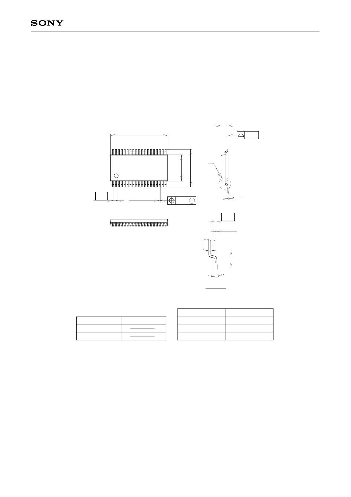
SONY CODE
EIAJ CODE
JEDEC CODE
PACKAGE MATERIAL
LEAD TREATMENT
LEAD MATERIAL
PACKAGE MASS
EPOXY RESIN
SOLDER PLATING
COPPER ALLOY
PACKAGE STRUCTURE
0.1g
TSSOP-38P-L121
38PIN TSSOP(PLASTIC)
0.1
0.1 M
0.225 ± 0.075
1
0.5
19
4.5 ± 0.2
6.4 ± 0.3
20
38
9.8 ± 0.2
0.15
A
1.2MAX
0.5 ± 0.1
0.05MIN
0° to 10°
DETAILA
0.25
Package Outline Unit : mm
CXA3238TN/CXA3239TN
—27—
 Loading...