

Page 1
Description
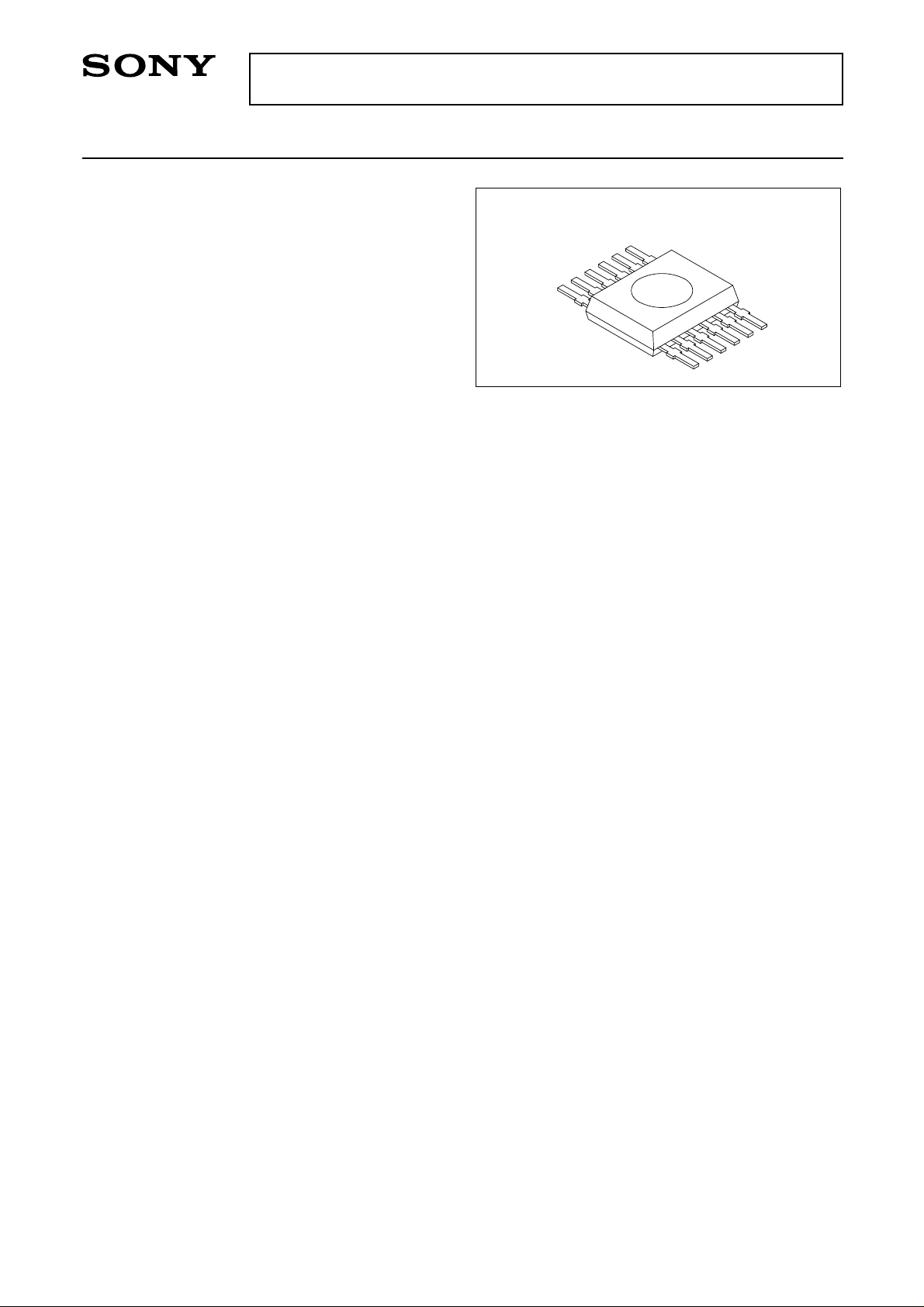
The CXA2598M is a PDIC (photodetector IC)
developed as a photodetector for the optical pickup
of CD-R/RW. The photodiode and I-V amplifier operate
at high speed (100MHz). When the strong light is
emitted during write, the delay or ringing is not
occurred because the limiter circuit is included in the
I-V amplifier.
• Focus servo: astigmatic method
• Tracking servo: differential push-pull method
Features
• I-V amplifier (current-voltage conversion circuit)
• RF output of addition of A to D signals
• Wide band (100MHz typ.)
• Output limiter circuit
• Small transparent molded package (SOP)
Applications
Optical pickup for CD-R/RW
Structure
Bipolar silicon monolithic IC
Absolute Maximum Ratings (Ta = 25°C)
• Supply voltage VCC 5.5 V
• Operating temperature Topr –10 to +70 °C
• Storage temperature Tstg –40 to +85 °C
• Allowable power dissipation PD 300 mW
Operating Condition
Supply voltage V
CC 4.5 to 5.5 V
PDIC for CD-R/RW
– 1 –
E00342-PS
Sony reserves the right to change products and specifications without prior notice. This information does not convey any license by
any implication or otherwise under any patents or other right. Application circuits shown, if any, are typical examples illustrating the
operation of the devices. Sony cannot assume responsibility for any problems arising out of the use of these circuits.
CXA2598M
PD-S-12 (Plastic)
Page 2
– 2 –
CXA2598M
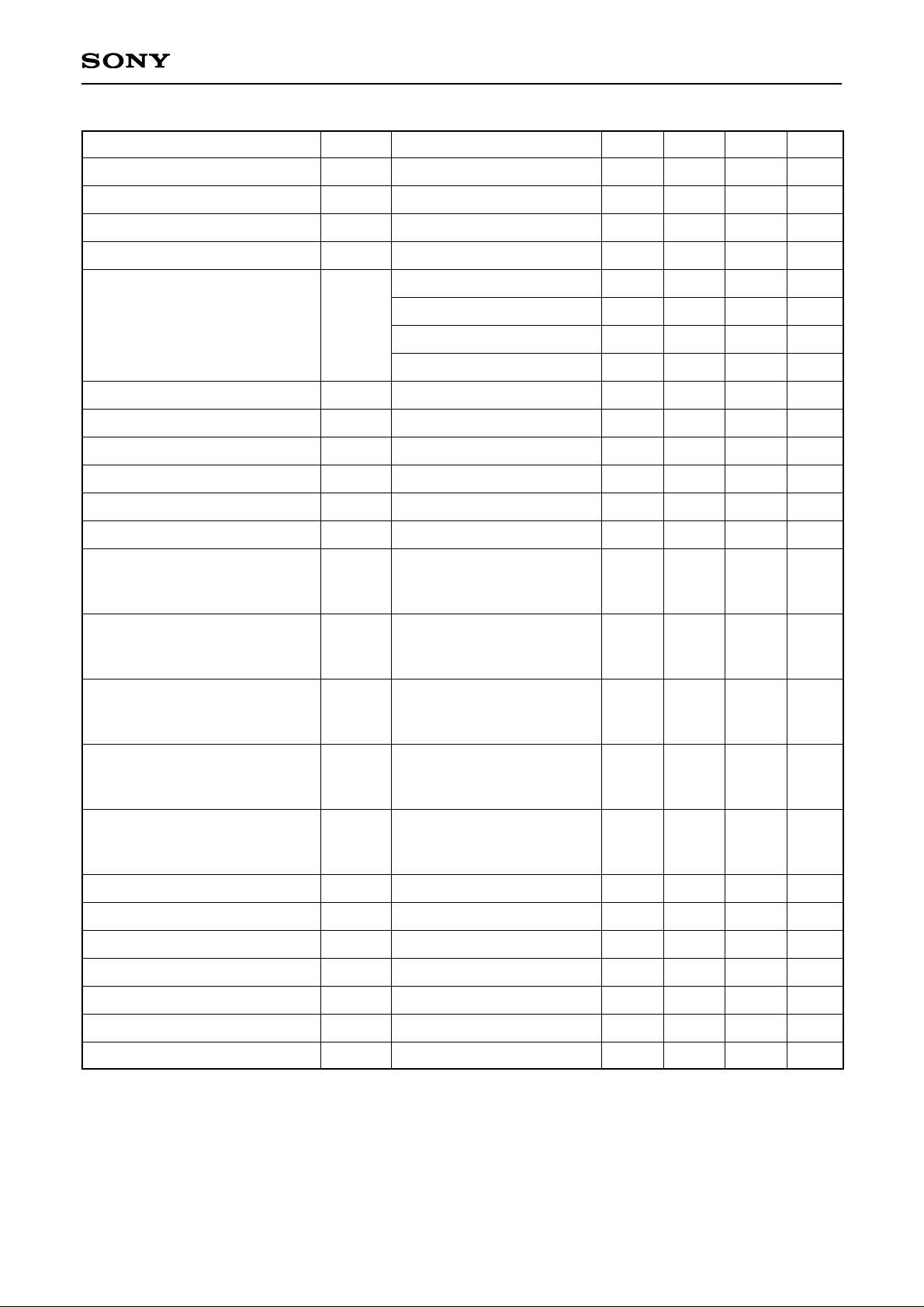
Electrical and Optical Characteristics (VCC = 5.0V, VC = 2.5V, Ta = 25°C)
Note 1) Output offset voltage: Vc is the reference.
Note 2) Output voltage: Vc is the reference. However, the offset voltage is excluded.
Note 3) Output voltage, offset temperature drift, frequency response, group delay difference, settling time,
slew rate: Confirmation of design.
Note 4) Measurement by the optical input: Measurement is made by emitting the light to the center of each
photodiode.
Item
Current consumption
Output offset voltage (A to D)
Output offset voltage (E to H)
Output offset voltage (RF)
Output offset voltage difference
Offset temperature drift (A to H)
Offset temperature drift (RF)
Output voltage (A to D)
Output voltage (E to H)
Output voltage (RF)
Maximum output voltage (A to H, RF)
Frequency response 1 (A to D)
Frequency response 1 (E to H)
Frequency response 1 (RF)
Frequency response 2 (A to D)
Frequency response 2 (RF)
Group delay difference (A to D)
Group delay difference (RF)
Settling time 1 (A to D)
Settling time 1 (E to H)
Settling time 2 (A to D)
Slew rate (A to D)
Slew rate (E to H)
Symbol
ICC
Voff
Voff
Voff
∆Voff
∆Voff/T
∆Voff/T
VO
VO
Vo
VO
fc
fc
fc
∆G
∆G
∆Gd
∆Gd
Tset1
Tset1
Tset2
SR
SR
Conditions
In the dark
In the dark, Vc reference
In the dark, Vc reference
In the dark, Vc reference
(A + B) – (C + D), in the dark
(A + D) – (B + C), in the dark
(A + C) – (B + D), in the dark
(E + G) – (F + H), in the dark
In the dark
In the dark
λ = 780nm, Po = 10µW
λ = 780nm, Po = 10µW
λ = 780nm, Po = 10µW
λ = 780nm, Po = 500µW
λ = 780nm
Po = 10µWDC, 4µWp-p
100kHz reference, –3dB
λ = 780nm
Po = 10µWDC, 4µWp-p
100kHz reference, –3dB
λ = 780nm
Po = 10µWDC, 4µWp-p
100kHz reference, –3dB
λ = 780nm
Po = 10µWDC, 4µWp-p
35MHz/100kHz
λ = 780nm
Po = 10µW
DC, 4µWp-p
35MHz/100kHz
100kHz to 35MHz
100kHz to 35MHz
Output 500mV → 5mV
Output 500mV → 5mV
Output 500mV → 0.5mV
—
—
Min.
—
–30
–25
–100
–20
–20
–20
–20
–100
–1.0
82
338
165
3.9
60
12
60
–0.5
–1.0
—
—
—
—
—
200
40
Typ.
16
0
0
0
0
0
0
0
—
—
110
450
220
4.0
100
20
100
0
0.5
0.5
0.5
—
—
—
—
—
Max.
25
30
25
100
20
20
20
20
100
1.0
138
563
275
—
—
—
—
0.5
1.0
2
2
40
70
70
—
—
Unit
mA
mV
mV
mV
mV
mV
mV
mV
µV/°C
mV/°C
mV
mV
mV
V
MHz
MHz
MHz
dB
dB
ns
ns
ns
ns
ns
V/µs
V/µs
Page 3
– 3 –
CXA2598M
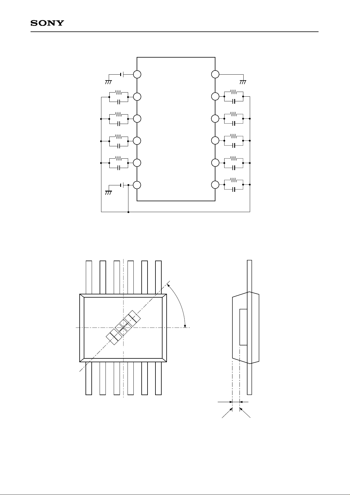
Measurement Circuit
1
2
3
4
5
7
8
9
10
11
12
6
Vcc
Vcc
Ho
Ao
Bo
Fo
Vc
Vc
GND
Go
Do
Co
Eo
RF
∗
All loads are 2.5kΩ//20pF.
Photodetector Position
H
12
Top view
7
16
GD
A
CFE
B
Center of package
45 deg.
0.52
Reference
surface
Surface that senses
the indident light
(Unit : mm)
Deviation from the center of photodetector
X, Y : ±0.2
Z: ±0.2
θ : ±2°
Page 4
– 4 –
CXA2598M
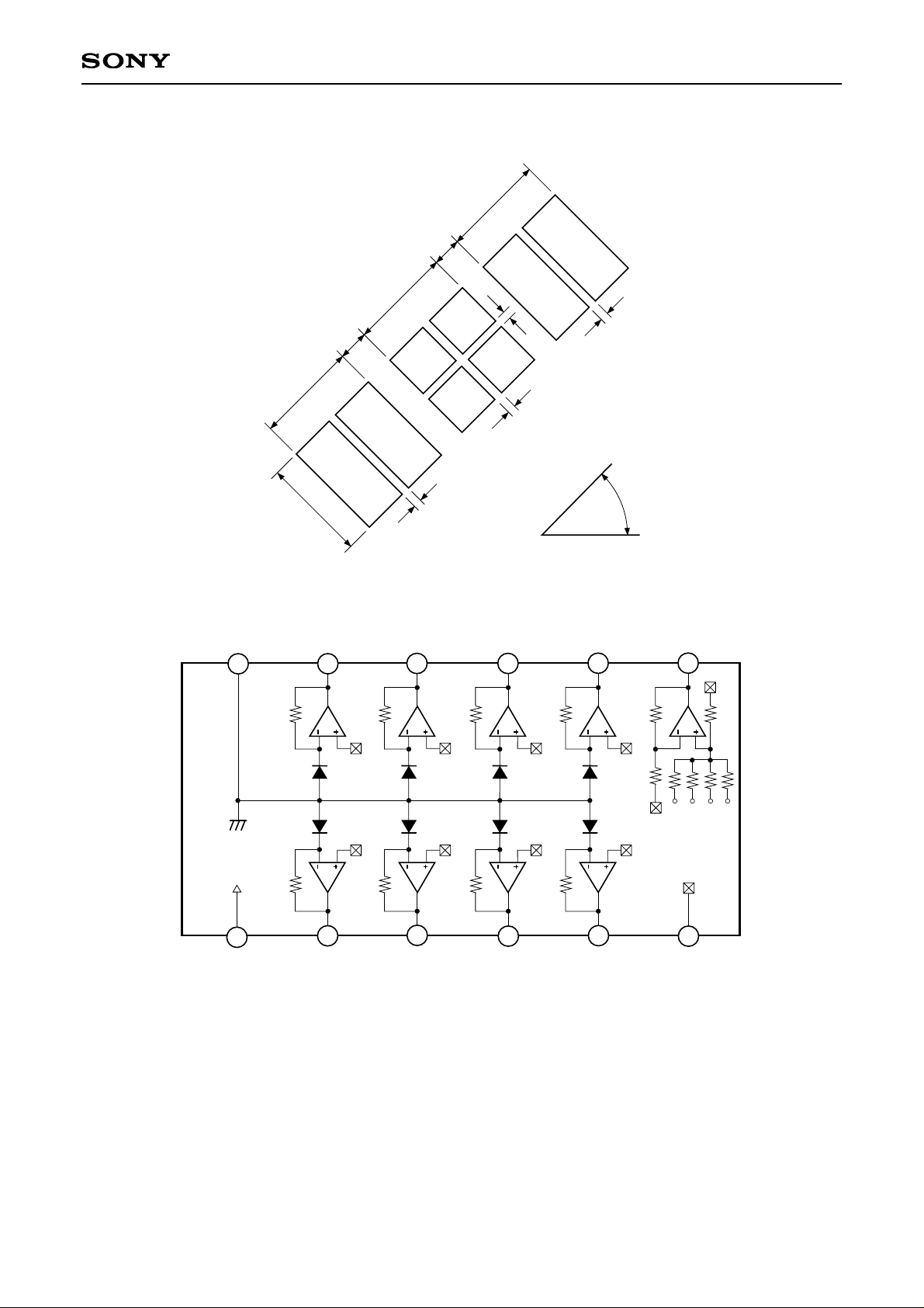
Photodetector Pattern Dimensions (Unit: µm)
555
5
160
160
HG FE
DC
AB
16040 16040
45 deg.
Circuit Block Diagram
1
2
3
4
5
6
7
8
910
11
12
R2
R2
E
AoBoCoDo
F
C
B
R1
R1
D
A
R1
R1
G
H
R2
GND Go Do Co Eo RF
VCC Ho Ao Bo Fo Vc
R2
R1 = 29kΩ, R2 = 118kΩ
A, B, C, D, E, F, G and H are the photodiodes. (Optical sensitivity: Approximately 0.40A/W)
Page 5
– 5 –
CXA2598M
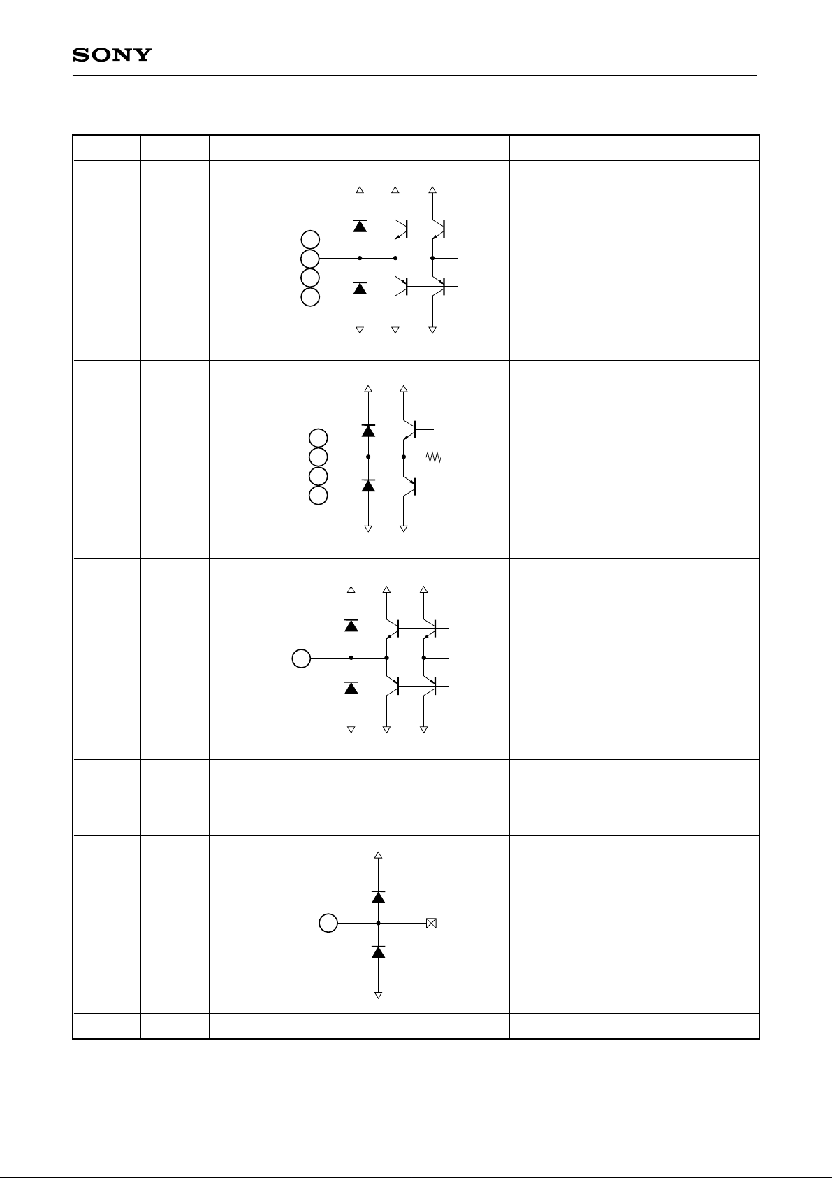
Pin Description
Pin No.
3
4
9
10
Symbol
Ao
Bo
Co
Do
I/O Equivalent circuit Description
O
Output of voltage signals converted
from optical signals
3
4
9
10
2
5
8
11
Ho
Fo
Eo
Go
O
Output of voltage signals converted
from optical signals
118k
2
5
8
11
6VC I
For dual power supply
: GND
For a single power supply
: center voltage input
6
12 GND
For dual power supply
: negative power supply
For a single power supply
: GND
1VCC I Positive power supply
7 RF O Output of addition of Ao to Do signals
7
Page 6
– 6 –
CXA2598M
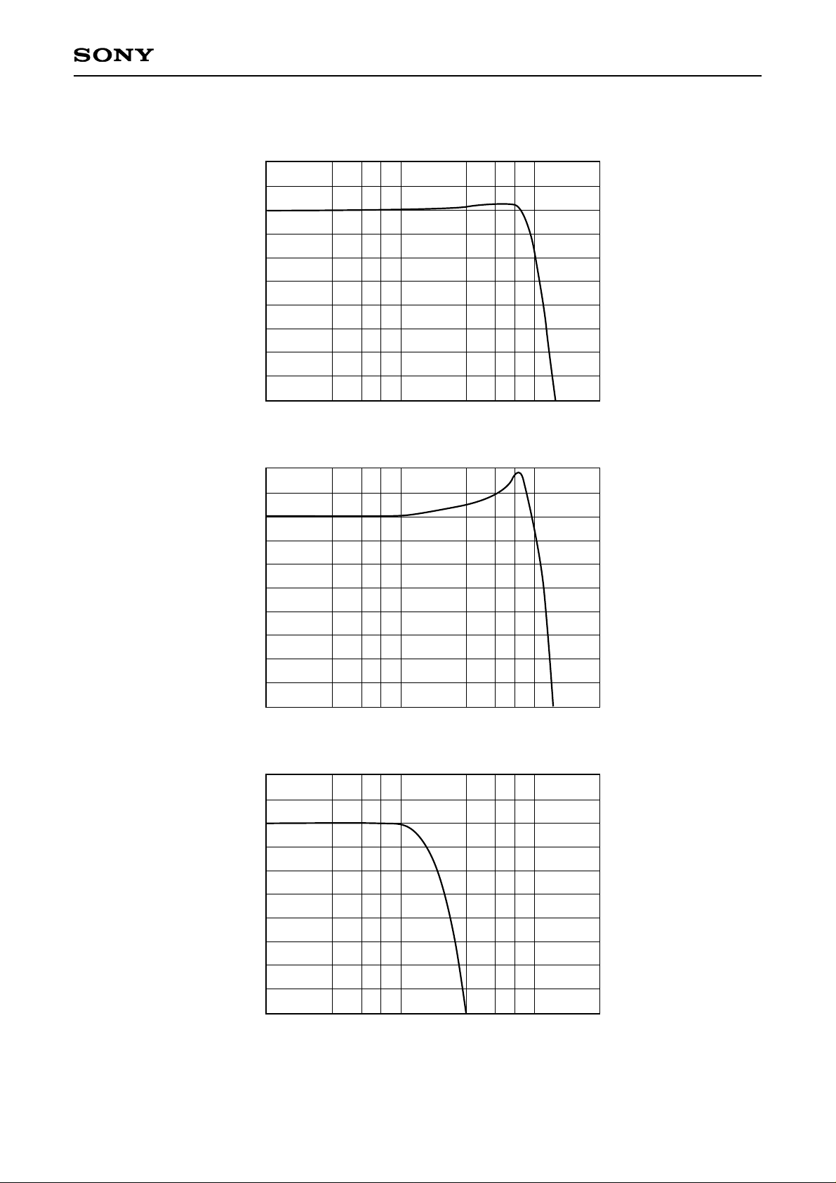
Example of Representative Characteristics
2
0
–2
Gain [dB]
–4
–6
–8
1 3 5 7 10 30
50 70 100
300
A to D I-V output frequency response
Frequency [MHz]
2
0
–2
Gain [dB]
–4
–6
–8
1 3 5 7 10 30
50 70 100
300
RF output frequency response
Frequency [MHz]
2
0
–2
Gain [dB]
–4
–6
–8
1 3 5 7 10 30
50 70 100
300
E to H I-V output frequency response
Frequency [MHz]
Page 7

– 7 –
CXA2598M
Notes on Operation
1. Connection to RF amplifier
The voltage input-type RF amplifier should be used because the CXA2598M is the voltage output type. The
noise allowance is dramatically increased compared to the case where the conventional photodiode and the
current input-type RF amplifier are used.
2. Power supply
The CXA2598M can be used with a single power supply or dual power supply. However, this IC is not provided
with a center voltage generating circuit, and so when used with a single power supply the center voltage must
be supplied from the RF amplifier or some other device.
Dual power supply
Single power supply
(Pin 1) VCC
Positive power supply
Positive power supply
(Pin 12) GND
Negative power supply
GND
(Pin 6) VC
GND
Center voltage
The potential difference between the Vcc pin and the GND pin should be in the range of 4.5 to 5.5V in both of
a single power supply and dual power supply.
3. Soldering
The reflow soldering is not guaranteed for the CXA2598M.
4. Mechanical strength for package
The mechanical strength for the package is not guaranteed for the CXA2598M.
Do not employ the mounting method which gives much weight to the package.
5. Visual inspection standard
Another specifications and limit samples must be exchanged regarding visual inspection standards for the
photodetector.
Page 8
– 8 –
CXA2598M
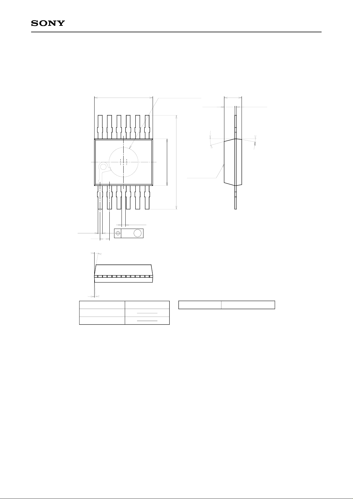
Package Outline Unit: mm
SONY CODE
EIAJ CODE
JEDEC CODE
M
PACKAGE MASS
0.05g
PD-S-12
PD-S-12
0.16
5.0 – 0.1
+ 0.4
12
7
1
6
0.3 MIN
0.8
0.3 ± 0.1
φ2.5 Mirror Surface
4.0
– 0.1
+ 0.3
8.0
±
0.4
Datum Plane
15
˚
10˚
0.15 – 0.05
+ 0.1
1.5 ± 0.1
0.9 ± 0.1
5˚
10˚
Sony Corporation
 Loading...