

Page 1

—1—
E96X14A8Z
Sony reserves the right to change products and specifications without prior notice. This information does not convey any license by
any implication or otherwise under any patents or other right. Application circuits shown, if any, are typical examples illustrating the
operation of the devices. Sony cannot assume responsibility for any problems arising out of the use of these circuits.
Absolute Maximum Ratings
• Supply voltage VCC 7.0 V
• Operating temperature Topr –20 to +75 °C
• Storage temperature Tstg –65 to +150 °C
• Allowable power dissipation
PD 417 mW
Operating Condition
Supply voltage VCC1 1.1 to 4.0 V
VCC2 2.5 to 4.0 V
Description
The CXA3176N is a low current consumption FM
IF amplifier which employs the newest bipolar
process. It is suitable for FM receiver using AFC.
Features
• Low current consumption :
0.95 mA (typ. at VCC1=1.4 V)
0.15 mA (typ. at VCC2=3.0 V)
• Small package 24-pin SSOP
• Second mixer and oscillator
• Needless of IF decoupling capacitor
• Reference power supply for operational amplifier
• RSSI function (dynamic range of 70 dB)
• IF input, VCC standard
• AFC function
• Maximum input frequency : 30 MHz
Applications
• FM receiver supporting AFC
• Double conversion FM receiver
Structure
Bipolar silicon monolithic IC
Block Diagram and Pin Configuration
IF Amplifier for FM Receiver (AFC Supported)
24 pin SSOP (Plastic)
CXA3176N
OSC
MIX
REG
LVA
IF_LIM
AFC
×4
QUAD_DET
22dB
RSSI
FILTER
GND
1 2 3 4 5 6 7 8 9 121110
OSC IN
OSC OUT
MIX OUT
V
CC
1
IF IN
AFC
AFC_C
QUAD
C1
C2
C3
RSSI_C
MIX IN
GND
REG OUT
REG CONT
LVA OUT
V
CC
2
CHARGE
B.S.
AUDIO
NC
AMP_OUT
RSSI
20 19 18 17 16 15 14 1324 23 22 21
Page 2

—2—
CXA3176N
Pin Description
Pin
Symbol
Pin
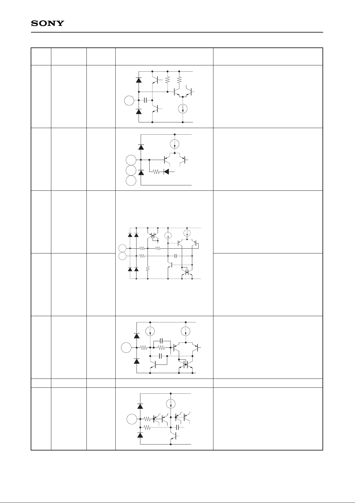
Equivalent circuit Description
No. voltage
1
2
3
4
5
6
7
OSC IN
OSC OUT
MIX OUT
VCC1
IF IN
AFC
AFC_C
1.4 V
0.7 V
1.3 V
1.4 V
—
—
Connects the external parts of crystal
oscillator circuit.
A capacitor and crystal oscillator are
connected to these pins and VCC.
Mixer output.
Connect a 450 kHz ceramic filter
between this pin and IF IN.
Power supply 1.
IF limiter amplifier input.
AFC output.
Connects the capacitor that becomes
the AFC time constant.
VCC
300
15k
GND
72
15k
2
1
3
VCC
GND
1.5k
VCC
1.5k
GND
1.5k520k 20k
VCC
GND
6
7
Page 3
—3—
CXA3176N
Pin
Symbol
Pin
Equivalent circuit Description
No. voltage
8
9
10
11
12
13
14
15
16
QUAD
C1
C2
C3
RSSI_C
RSSI
AMP OUT
NC
AUDIO
1.4 V
0.2 V
0.1 V
0.1 V
VCC2/2
—
0.2 V
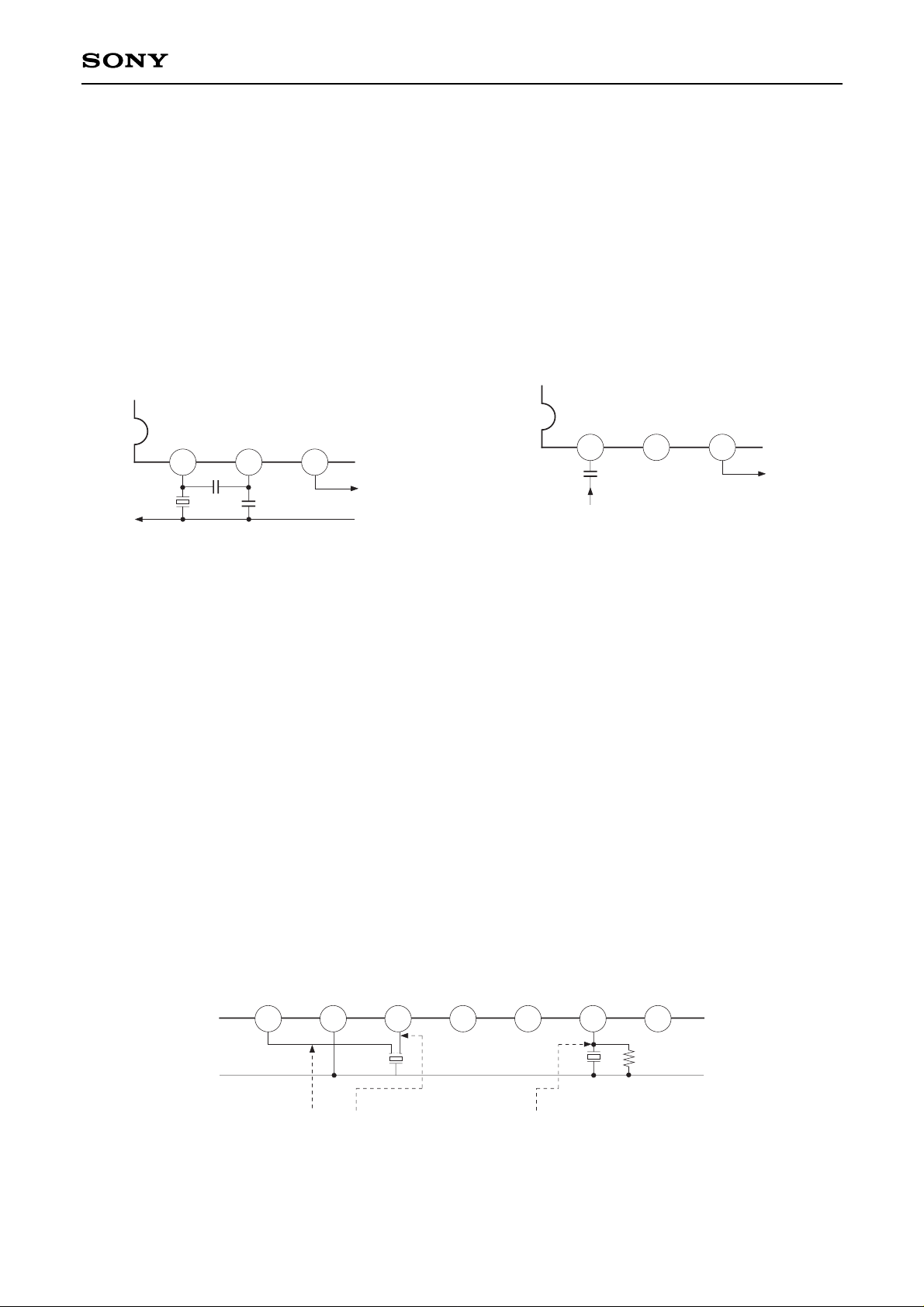
Connects the phase shifter of FM
detector circuit.
Connects the capacitor that determines
the LPF cut-off.
Connects the capacitor that determines
the RSSI rising characteristics.
RSSI circuit output.
Output for the detector output
amplification circuit.
Not connected.
Input for the detector output
amplification circuit and AFC circuit.
The filter circuit output is connected.
8
VCC
22k
GND
20p
20k
VCC
GND
10
11
9
35k
VCC
GND
12
13
VCC
GND
14
VCC
GND
16
Page 4

—4—
CXA3176N
Pin
Symbol
Pin
Equivalent circuit Description
No. voltage
17
18
19
20
21
22
23
24
B.S.
CHARGE
VCC2
LVA OUT
REG
CONT
REG OUT
GND
MIX IN
—
—
—
—
—
1.0 V
—
1.4 V
Controls the battery saving.
Setting this pin low suspends the
operation of IC.
(Applied voltage range :
–0.5 V to +7.0 V)
Controls the time constant of the AFC
circuit.
Set this pin high to make the short time
constant.
(Applied voltage range:
–0.5 V to +7.0 V)
Power supply 2.
LVA comparator output.
It is open collectors.
(Applied voltage range:
–0.5 V to +7.0 V)
Output for internal constant-voltage
source amplifier.
Connect the base of PNP transistor.
(Current capacity : 100 µA)
Constant-voltage source output.
Controlled to maintain 1.0 V.
Ground
Mixer input.
20k
100k
GND
18
72
20k
140k
GND
17
72
GND
20
21
VCC
GND
72
VCC
GND
78k
1k
22k
22
VCC
GND
2k
4.16k
4.16k
24
Page 5

—5—
CXA3176N
Item
Current consumption1
Current consumption2
Current consumption
AM rejection ratio
VB output current
VB output saturation voltage
REG OUT voltage
LVA operating voltage
LVA output leak current
LVA output saturation voltage
Logic input voltage high level
Logic input voltage low level
Limiting sensitivity
RSSI output offset
Mixer input resistance
Mixer output resistance
IF limiter input resistance
AMP OUT
Electrical Characteristics
(VCC1=1.4 V, VCC2=3 V, Ta=25 °C, FS=21.7 MHz, FMOD=4 kHz, FDEV=4.5 kHz, AMMOD=30 %)
Symbol
ICC1
ICC2
ICCS
AMRR
IOUT
VSATVB
VREG
VLVA
ILLVA
VSATLVA
VTHBSV
VTLBSV
VIN (LIM)
VORSSI
RINLIM
ROUTMIX
RINLIM
VAMP
Conditions
Measurement circuit 1, V2=1.0 V
Measurement circuit 1, V2=1.0 V
Measurement circuit 1, V2=0 V
Measurement circuit 2, 30 k LPF
Measurement circuit 3
Measurement circuit 3
Output current 0 µA
Measurement circuit 4,
V1=1.4 to 1.0 V
Measurement circuit 4, V1=1.0 V
Measurement circuit 5
—
—
Measurement circuit 2,
Data filter fc=6.2 kHz
Measurement circuit 6
—
—
—
Measurement circuit 2
Typ.
0.95
0.15
6
—
—
—
0.97
1.05
—
—
—
—
–108
150
2.0
1.5
1.5
630
Max
1.35
0.25
10
—
—
0.4
1.02
1.10
2.0
0.4
—
0.35
—
300
2.4
1.8
1.8
800
Unit
mA
mA
µA
dB
µA
V
V
V
µA
V
V
V
dBm
mV
kΩ
kΩ
kΩ
mVrms
Min.
0.5
—
—
25
100
—
0.92
1.00
—
—
0.9
—
—
—
1.6
1.2
1.2
500
Page 6

—6—
CXA3176N
Electrical Characteristics Measurement Circuit
Measurement circuit 2
Measurement circuit 4
Measurement circuit 6
Measurement circuit 1
Measurement circuit 3
Measurement circuit 5
VCC
V1
1.4V
V3
3.0V
20 19 18 17 16 15 14 1324 23 22 21
A
A
V2
V
V4
1 2 3 4 5 6 7 8 9 10 1211
VCC
V1
1.4V
V3
3V
V2
1.0V
GND
V3
0.5V
GND
V
20 19 18 17 16 15 14 1324 23 22 21
1 2 3 4 5 6 7 8 9 10 1211
100µA
VCC
V3
3V
V2
1.0V
1 2 3 4 5 6 7 8 9 10 1211
V
V1
1.4V
50µA
20 19 18 17 16 15 14 1324 23 22 21
22p
15p
1µ 5.6k
1200p
1200p
1200p
1 2 3 4 5 6 7 8 9 10 1211
V
CC
V1
1.4V
1000p
10p to
120p
Vin
1.8µ
V3
3.0VV21.0V
V
20 19 18 17 16 15 14 1324 23 22 21
VCC
V3
3V
V2
1.0V
V1
1.4 to 1.0V
1 2 3 4 5 6 7 8 9 10 1211
V
100k
A
20 19 18 17 16 15 14 1324 23 22 21
VCC
V3
3V
V2
1.0V
V1
1.4V
100p
1 2 3 4 5 6 7 8 9 10 1211
V
20 19 18 17 16 15 14 1324 23 22 21
Page 7

—7—
CXA3176N
Application Circuit
GND
OSC
MIX
REG
LVA
IF_LIM
AFC
×4
QUAD_DET
22dB
RSSI
FILTER
GND
RF SMA
10P to 120P
1.8µH
GND
1000P
GND
GND
10µ
PNP
P7
REG
S2
100k
P6
LVA
GND
S1
P5
V
CC
2
10µ
GND
0.01µ
P4
AMP_OUT
P3
RSSI
BS AUDIOVB_REG
100P
GND
470P
GND
470P
470P
GND
P1
V
CC
GND
DISK
5.6K
1µ
P2
AFC
CERAFIL
GND
10µ
0.01µ
1 2 3 4 5 6 7 8 9
121110
15P
XTAL
22P
20 19 18 17 16 15 14 1324 23 22 21
C2
L1
C3
C6
R4
C9
C10
C15
C14
C13
C12
C11
R5
C8
C7
C5
C4
Application circuits shown are typical examples illustrating the operation of the devices. Sony cannot assume responsibility for
any problems arising out of the use of these circuits or for any infringement of third party patent and other right due to same.
Page 8
—8—
CXA3176N
Application Notes
1) Power Supply
The CXA3176N, with built-in regulator, is designed to permit stable operation at a wide range of supply
voltage of VCC1=1.1 to 4.0 V and VCC2=2.5 to 4.0 V. Decouple the wiring to VCC (Pins 4 and 19) as close
to the pin as possible.
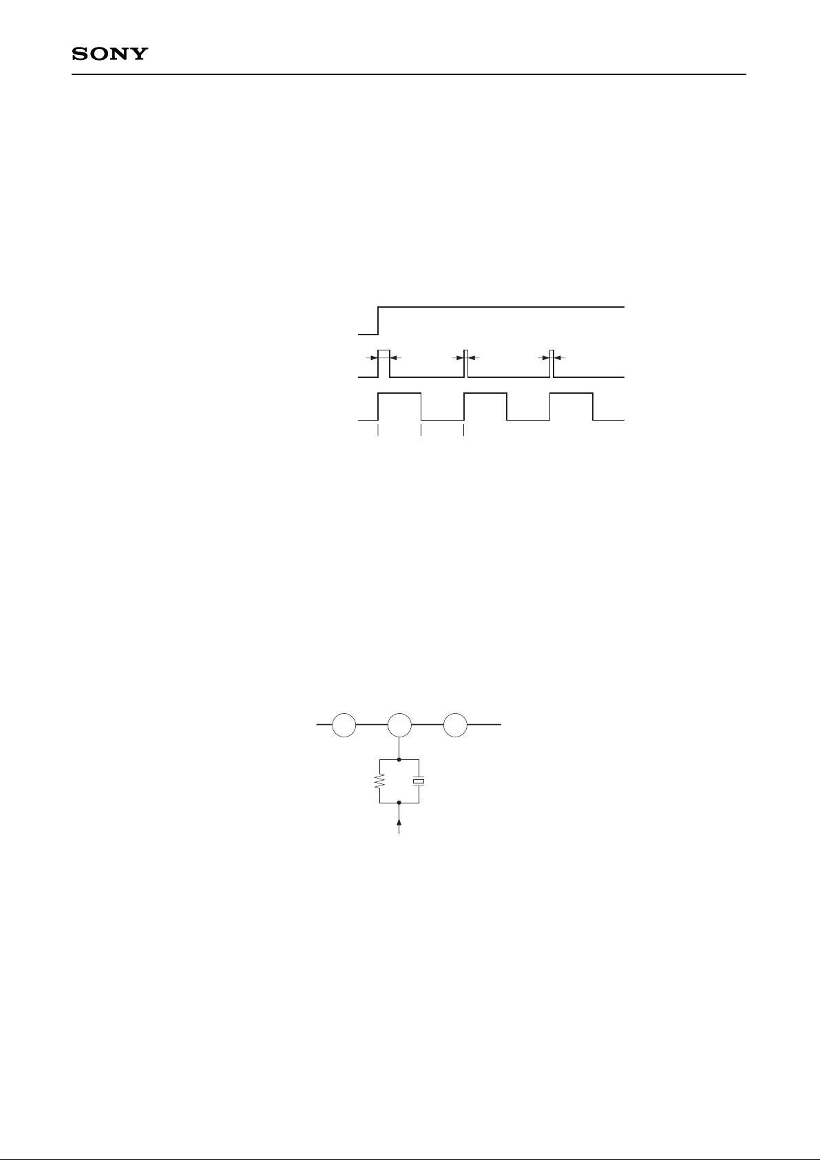
2) Oscillator Input
Oscillator input method
a) Using Pins 1 and 2, input a self-excited oscillation signal through the composition of a Colpitts type
crystal oscillator circuit.
b) Directly input a local oscillation signal to Pin 1.
3) Mixer
The mixer is of double-balance type. Pin 24 is the input pin. Input though a suitable matching circuit. The
input impedance is 2.0 kΩ.
Pin 3 serves as the output pin for the mixer, and a load resistance of 1.5 kΩ is incorporated.
4) IF Filter
The filter to be connected between this mixer output and the IF limiter amplifier input should have the
following specifications.
I/O impedance : 1.5 kΩ ±10 %
Band width : Changes according to applications.
5) IF Limiter Amplifier
The gain of this IF limiter amplifier is approximately 100 dB. Take notice of the following points in making
connection to the IF limiter amplifier input pin (Pin 5).
a) Wiring to the IF limiter amplifier input (Pin 5) should be as short as possible.
b) As the IF limiter amplifier output appears at QUAD (Pin 8), wiring to the ceramic discriminator
connected to QUAD should be as short as possible to reduce the interference with the mixer output and
IF limiter amplifier input.
1 2 3
VCC
Ceramic
filter
1 2 3
From
local signal
Ceramic
filter
Fig. 1
VCC
3 4 5 6 7 8 9
Wire as short and apart as possible As short as possible
Fig. 2
Page 9
—9—
CXA3176N
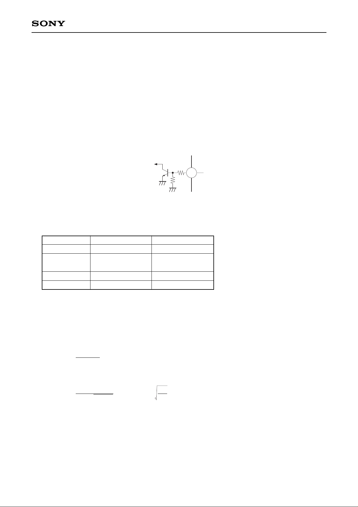
6) Quick Charge
In order to hasten the rise time of Pin 7 from when power is turned on, the CXA3176N features a quick
charge circuit. The capacitance value connected to Pin 7 should be chosen such that the voltage does not
vary much due to discharge during battery saving.
Connect a signal for controlling the quick charge circuit to Pin 18. Setting this pin high enables the quick
charge mode, and setting this pin low enables the steady-state reception mode. Quick charge is used
when the power supply is turned on. The battery saving must be set high at the time.
Connect Pin 18 to GND when quick charge is not being used.
7) Detector
The detector is of quadrature type. To perform phase shift, connect a ceramic discriminator to Pin 8.
The phase shifting capacitor for the quadrature detector is incorporated. The FM signal demodulated with
the detector will be output to AMP_OUT (Pin 14) through the internal LPF.
The CDBC450CX50 (MURATA MFG. CO., LTD.) ceramic discriminator is recommended for the
CXA3176N.
Fig. 3
Fig. 4
5.6k
VCC
7 8 9
Ceramic
discriminator
CDBC450CX50
H
L
H
L
active
battery
saving
5ms 1ms 1ms
Power supply
(Pin 4)
Quick charge
(Pin 18)
Battery saving
(Pin 17)
Timing
Page 10
—10—
CXA3176N
8) REG CONT
Controls the base bias of the external transistors.
9) LVA OUT
This pin goes high (open) when the supply voltage becomes lower. Since the output is an open collector, it
can be used to directly drive the CMOS device. The setting voltage of the LVA is 1.05 V (typ.), and it
possesses a hysteresis with respect to the supply voltage. The hysteresis width is 50 mV (typ.).
10) B.S.
Operation of the CXA3176N can be halted by setting this pin low. This pin can be connected directly to the
CMOS device. The current consumption for battery saving is 10 µA or less (at 1.4 V).
11) Control Pins
The function controls are as shown below.
Note) When each function is not controlled externally, set it to the state with an asterisk (∗).
12) LPF Constant
The composition of the data filter is ternary.
The first-stage cut-off fC1 is
1
fC1 =
2πC12R
The second-stage cut-off fC2 is
1 C13
fC2 =
2πR√C13 C14
, Q =
C14
C12, C13, C14 : External capacitance shown in the Application Circuit
R : IC internal resistance
The Butterworse characteristic is for C12=C13=C14.
R is approximately 55 kΩ ±20 %.
17
B.S.
Fig. 5
Pin No.
Symbol
Function
Input high
Input low
17
B.S.
Battery saving
mode control
IC operation
∗
Sleep
18
CHARGE
Pin 7 charge
speed control
Quick charge
Slow charge
∗
Page 11
—11—
CXA3176N
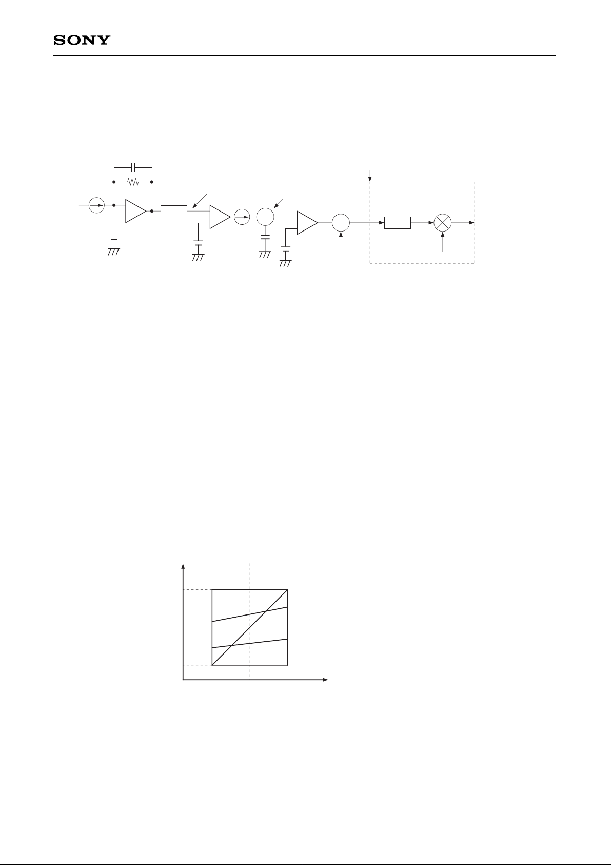
13) AFC
The AFC is of the current output type which outputs the frequency deviation in the form of the current and
converts it to the voltage. The output current range is approximately ±0.4 µA for the slow mode and ±70
µA for the fast mode.
CXA3176N AFC Principle Diagram
The Pin 7 voltage V continues to change till the Vin value reaches the Vref value. When these values are
equal, the Pin 7 output current becomes “0” and the voltage is determined by the charge and time.
The Pin 7 voltage V is output to Pin 6 through the amplifier.
Vout=Vref+4 (V–Vref)
The Vout operating range is 0.4 V to 4 (VCC–0.2) V so that AFC should be set within this range.
Also, the voltage for Pin 7 is undefined with the IC itself.
The AFC voltage varies, for example, as shown below by the VCO characteristics. The AFC voltage
follows the VCO characteristics because this voltage is independent of the slope of the S curve. In other
words, the CXA3176N operates according to the VCO characteristics when the VCO characteristics have
the linearity with respect to the voltage and the VCO characteristics can be controlled within the range
shown in the graph below.
Vref
Vref
C
V=it/C
×4
LPF
Vref
BUF
7
6
VCO
RF
Vin (S curve voltage)
Vout
(AFC voltage)
External parts
1st MIX for
FM receiver
1st OSC for
FM receiver
To CXA3176N
4 (VCC–0.2)V
0.4V
fo
A
B
C
Pin 6 voltage
Input frequency
Page 12

—12—
CXA3176N
14) Sensitivity Adjustment Method
The constants shown in the Application Circuit are for the standard external parts. However, adjustment
may be necessary depending on the conditions of use, characteristics of external parts, and the RF system
circuit and decoder connected to the IF IC, etc. Adjust the sensitivity according to the following
procedures.
a) MIX IN matching
When using a matching circuit between the RF system circuit and MIX IN of the CXA3176N, adjust the
trimmer to obtain the optimal sensitivity while monitoring the AUDIO output.
b) Local input level
The mixer circuit gain is dependent on the local signal input level to OSC IN. The input level to OSC IN
should be set as high as possible within the range of –6 to +2 dBm as shown in the graph of “Local input
level vs. Mixer gain characteristics”. However, care should be taken as raising the input level above +2
dBm will cause the sensitivity to drop.
When creating the local signal using the internal oscillator circuit, the oscillation level varies according to
the external capacitances attached to Pins 1 and 2 and the characteristics of the used crystal. Therefore,
be sure to adjust the external capacitance values attached to Pins 1 and 2 according to the crystal
characteristics.
C1 and C2 have the following range in the figure above.
C1 ≥ C2
C1 = C2 to C1 =5C2
As for the ratio of C1 to C2, the oscillation stabilizes as C1 approaches equality with C2.
The oscillation level decreases as the C1 and C2 values become larger, and increases as the C1 and C2
values become smaller.
Use a FET probe to confirm the local input level.
c) LPF constant (when the CXA3176N is used for the pager)
The data filter cut-off may need to be changed depending on the characteristics of the connected decoder.
Adjust the capacitance values of Pins 9 to 12 while checking the incoming sensitivity including the decoder.
If the capacitance values are too large, the detector output waveform will deviate at high data rates,
causing the sensitivity to drop. Conversely, if the capacitance values are too small, the LPF will be easily
affected by noise, causing the sensitivity to drop.
Adjust capacitance values of Pins 9 to 12 so that the capacitance value described in “12) LPF Constant”
becomes smaller.
OSC
1 2
C1
C2
VCC
Page 13

—13—
CXA3176N
d) AFC
The CXA3176N uses the AFC to correct the IF frequency deviation. WHen the IF frequency deviation
amount is large, correction takes time and may lower the sensitivity. Adjust the oscillator frequency of the
local oscillator so that the center frequency of the signal input to Pin 5 (IF IN) is as close to 450 kHz as
possible.
15) CXA3176N Standard Board Description
• Outline
This board contains the external parts shown in the Application Circuit in order to evaluate the
CXA3176N operation
• Features
The following CXA3176N basic operations can be checked.
1) Battery saving and other mode switching
2) AFC pin
3) The RSSI pin output is the low impedance because it is output via the buffer.
• Method of use
1) Input the CXA3176N supply voltage VCC1=1.4 V and VCC2=3 V.
This IC operates with a single power supply.
2) The CXA3176N uses a 21.245 MHz crystal. Input the RF signal from the RF pin and use this IC in
the condition where IF=450 kHz.
3) The AFC pin voltage is undefined with the IC itself because the current output circuit is employed for
the AFC. For the evaluation, be sure to apply the bias externally to the AFC pin or to make the AFC
loop.
4) Set the mode switches.
• Mode switch setting
Mode switches S1 and S2 are provided in two locations in the board. Each basic operation can be
confirmed by switching these mode switches while referring to the board layout. See the table in “11)
Control Pins” for the mode switching.
• Device specification
See these specifications for the IC specifications. The ICs for this evaluation board are ES specification.
• Circuit diagram
The circuit diagram is the same as the Application Circuit in these Specifications.
Page 14

—14—
CXA3176N
15) -1. [Board Layout]
15) -2. [Mode Switch Pattern]
24 13
XTAL
1 12
CERAFIL
DISK
ON ON
OFF OFF
S2
S1
RF
PNP
VCC GND VCC2
GND
GND
3176
EVALUATION BOARD
Low
High
ON
OFF
S2
Slow
Quick
< CHARGE >
Low
High
ON
OFF
S1
Sleep
Active
< B.S. >
Page 15
—15—
CXA3176N
15) -3. List of Standard Board Parts
Resistor
Capacitor
Inductor
Active Component
Crystal
Ceramic Filter
Ceramic Discriminator
Value Part #
Remarks
(Manufacture)
Note
5.6 k
100 k
R5
R4
(RIVER)
E12 series
1/8W
1.8 µH L1
EL0405
(TDK Products)
E12 series
2.5 mm pitch
(Lead Pitch)
PNP
2SA1015
(TOSHIBA CORPORATION)
Vceo Ic Pc Hfe fc
–50 V –150 m 400 m70 to 40080 M
21.245 MHz XTAL
NR-18BN
(NIHON DEMPA KOGYO CO., LTD.)
CERAFIL
CFWS450D
(MURATA PRODUCTS)
450 kHz
1.5 kΩ
DISC
CDBC450CX50
(MURATA PRODUCTS)
450 kHz
6.8 P to 45 P
15 P
22 P
100 P
470 P
1000 P
0.01 µ
1 µ
10 µ
C2
C5
C4
C15
C12
C13
C14
C3
C8
C10
C11
C6
C7
C9
TZ03P450FR169
(MURATA PRODUCTS)
DD100 series
temperature characteristics
type B
(MURATA PRODUCTS)
RPE131F103Z50
(MURATA PRODUCTS)
25 V 1 µ
(SHIN-EI TUSHIN
KOGYO CO., LTD.)
25 V 10 µ
(SHIN-EI TUSHIN
KOGYO CO., LTD.)
TRIMMER CAPACITOR
CERAMIC CAPACITOR
E12 series
(high dielectric constant type)
MONOLITHIC CERAMIC CAPACITOR
RPE series
ELECTROLYTIC CAPACITOR
E6 series
Page 16
—16—
CXA3176N
Switch
Connector
Pin
S1
S2
ATE1D-2M3-10
(FUJISOKU CORPORATION)
ON-ON (1 poles)
AC/DC 48 V 50 mA Max.
AC/DC 20 mA 1 µA Min.
RF
HRM300-25
(HIROSE ELECTRIC CO., LTD.)
SMA CONNECTOR
× 5
× 6
Mac 8 test pin ST-1-3
(Mac eight)
Mac 8 test pin LC-2-G
(Mac eight)
L=10 mm 0.8 φ
Page 17

—17—
CXA3176N
1.2
1.1
1.0
0.9
0.8
0 1.0 2.0 3.0 4.0
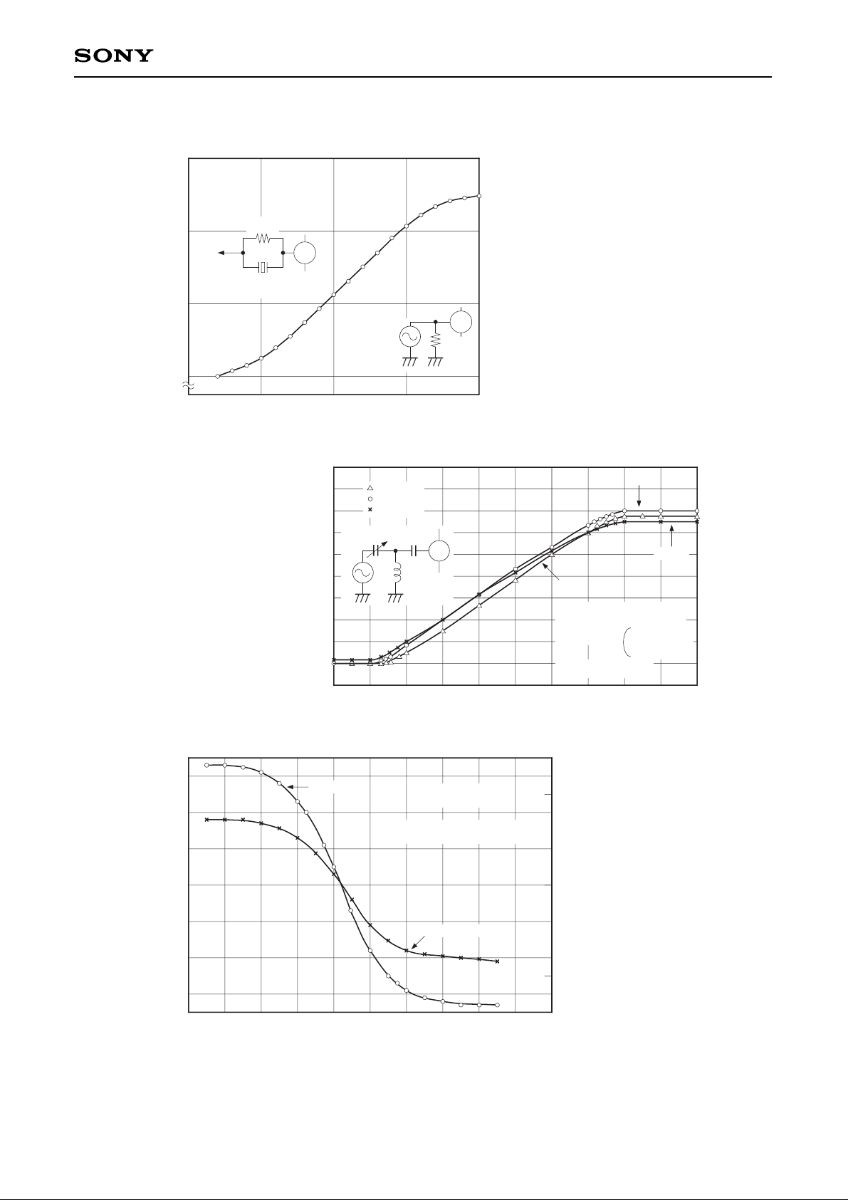
Current consumption characteristics
Supply voltage (V)
I
CC
1 (Pin 4) current (mA)
I
CC
2 (Pin 19) current (mA)
10
20
30
40
50
–120
Mixer input audio response and RSSI characteristics
RF input level (dBm)
Audio response (dB)
RSSI output voltage (mV)
10
0
–10
–20 –10 0
Local input level vs. Mixer gain characteristics
Local input level (dBm)
Mixer gain (dB)
–110 –100 –90 –80 –70 –60 –50 –40 0
0
60
V
CC1 1.4V
VCC2 3.0V
RF 21.7MHz
–60dBm
Lo 21.25MHz
With IF filter load
Mixer gain is the level difference
between Pin 3 and Pin 24
500
1000
0.13
0.12
ICC1 (at VCC2 3.0V)
ICC2 (at VCC1 1.4V)
–30
VCC2 3.0V
RF 21.7MHz
VCC1 1.4V
fDEV 4.5kHz
fMOD 4kHz
Lo 21.25MHz 0dBm
0dB=630mVrms
T=25°C
S
S/N
RSSI
10P to 120P 1000P
24
1.8µ
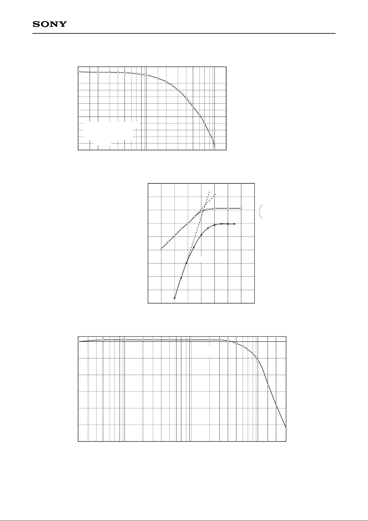
Example of Representative Characteristics
Page 18
—18—
CXA3176N
1.0
0
–10
1M 10M 100M
Mixer input frequency vs. Gain characteristics
Pin 24 input frequency (Hz)
Mixer gain (dB)
–20
–40
–60
–80
–60
Mixer I/O characteristics and 3rd-order intercept point
Pin 24 input level (dBm)
Pin 3 output level (dBm)
0
–10
100 1k 10k
Cut-off characteristics of audio filter
Input frequency (Hz)
Response (dB)
–40 –20 0
0
f1 + f2
fo
V
CC1 1.4V
VCC2 3.0V
fo 21.7MHz
f1 21.725MHz
f2 21.75MHz
Lo 21.25MHz 0dBm
with IF filter load
–20
–30
–40
–50
–60
VCC1 1.4V
VCC2 3.0V
VCC2 3.0V VCC1 1.4V
RF –60dBm
Lo (RF –0.45) MHz
0dBm
Page 19
—19—
CXA3176N
300
200
100
440 445 450 455 460
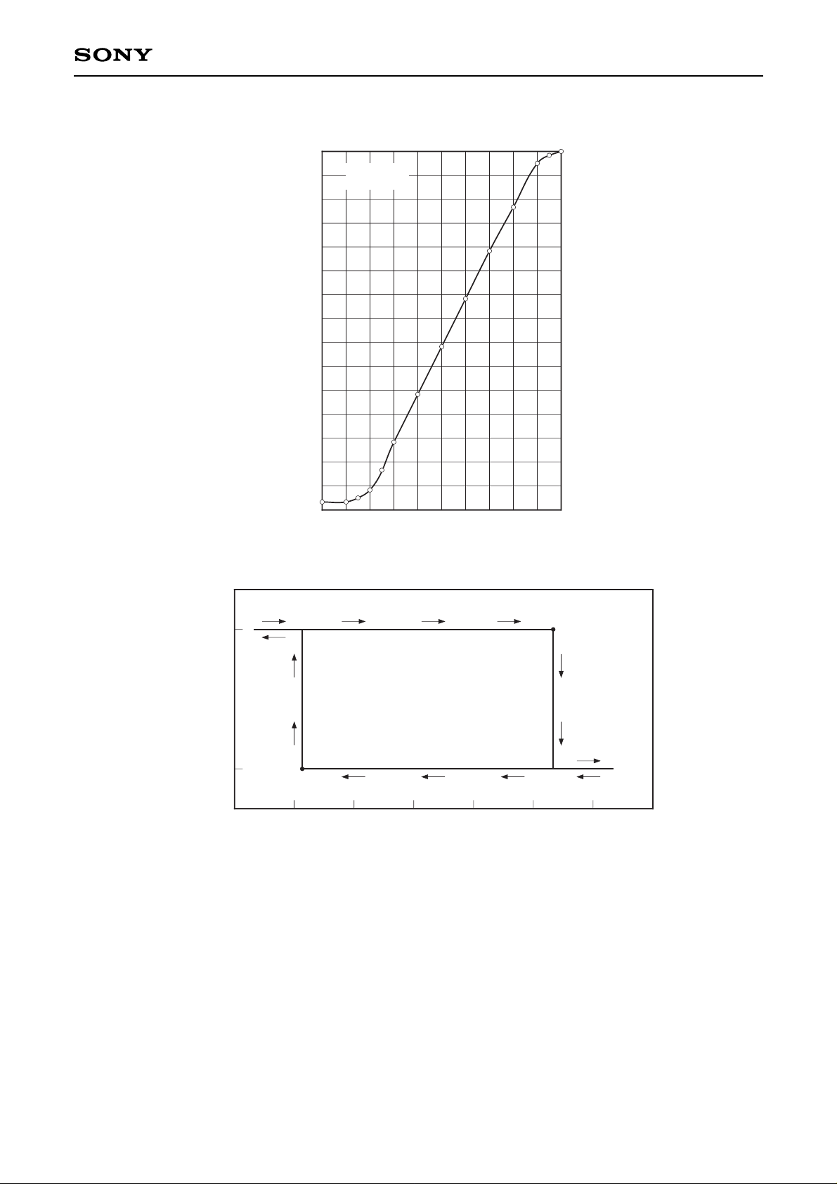
S curve characteristics
Pin 5 input frequency (kHz)
Pin 16 voltage (mV)
1000
500
–120
RSSI output voltage temperature chatacteristics
RF input level (dBm)
Pin 13 voltage (mV)
0.6
0.4
–0.2
80 120 160
AFC output current characteristics
Pin 16 voltage (mV)
Slow (Pin 7) current (µA)
–110 –100 –90 –80 –70 –60 –50 –40 –30
VCC1 1.4V
VCC2 3V
IF –40dBm
5
50
CDBC 450 CX50
(MURATA MFG. CO., LTD)
8
VCC1
4.7k
–20
25°C
–20°C
75°C
25°C
–20°C
…
…
…
24
1.8µ
10P to 120P 1000P
VCC1 1.4V
RF 21.7MHz
VCC2 3.0V
fDEV 4.5kHz
fMOD 4kHz
Lo 21.25MHz 0dB
200 240 280 320 360 400
0.2
0
–0.4
–0.6
–50
0
50
Fast mode
Slow mode
VCC1 1.4V
VCC2 3.0V
Pin 7 215mV fixed
(external power supply)
Fast (Pin 7) current (µA)
75°C
Page 20
—20—
CXA3176N
3
0 500 1000
AFC amplifier characteristics
Pin 7 voltage (mV)
Pin 6 voltage (V)
High
Low
1050
LVA characteristics
Pin 4 voltage (mV)
LVA comparator output voltage
1060 1070 1080 1090 1100 1110
2
1
VCC2 3.0V
VCC1 1.4V
VCC2 3.0V
Page 21
SONY CODE
EIAJ CODE
JEDEC CODE
SSOP-24P-L01
SSOP024-P-0056
PACKAGE MATERIAL
LEAD TREATMENT
LEAD MATERIAL
PACKAGE MASS
EPOXY RESIN
SOLDER/PALLADIUM
42/COPPER ALLOY
PACKAGE STRUCTURE
PLATING
0.1g
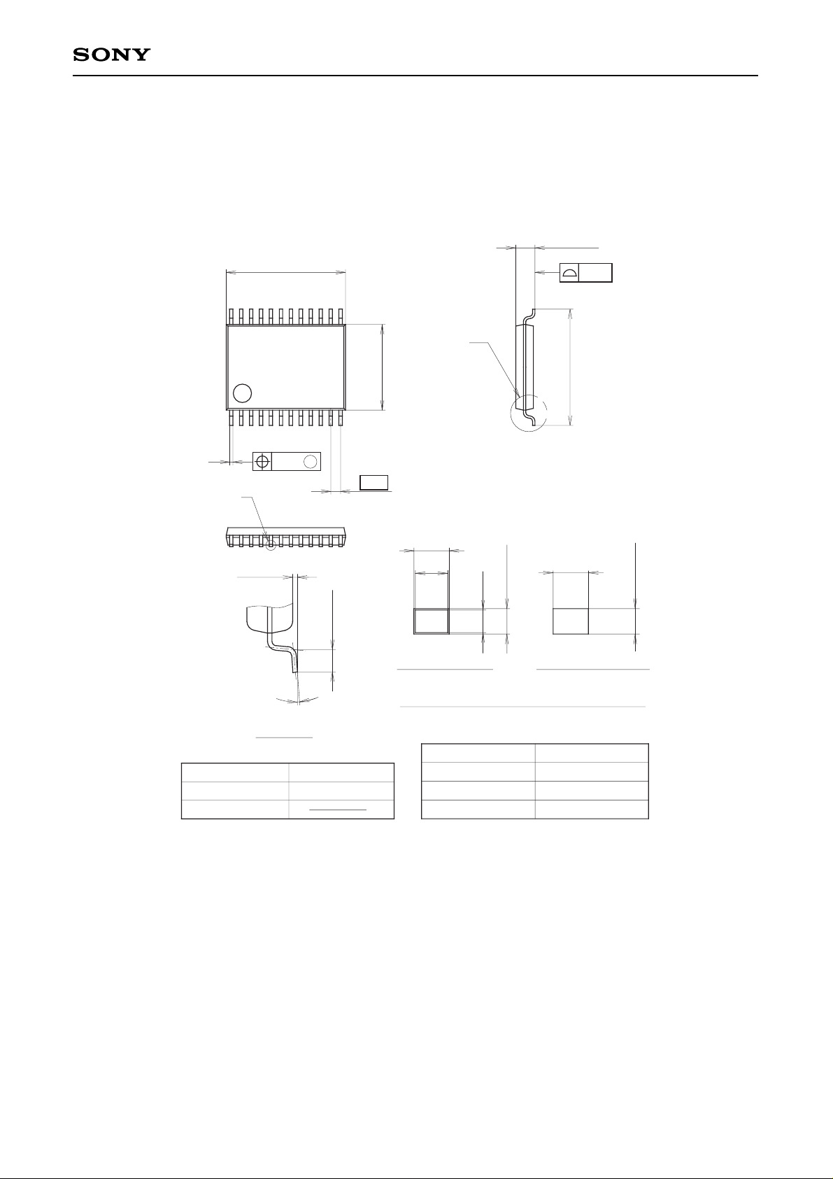
24PIN SSOP(PLASTIC)
0.1 ± 0.1
0° to 10°
0.5 ± 0.2
DETAIL
A
∗5.6 ± 0.1
24
∗7.8 ± 0.1
13
0.65
12
1
7.6 ± 0.2
0.1
1.25 – 0.1
+ 0.2
A
0.13
M
NOTE: Dimension “∗” does not include mold protrusion.
b=0.22 – 0.05
+ 0.1
0.15 – 0.02
+ 0.05
(0.22)
(0.15)
0.15 – 0.01
DETAIL B : SOLDER DETAIL B : PALLADIUM
+ 0.03
b=0.22 ± 0.03
B
b
Package Outline Unit : mm
CXA3176N
—21—
NOTE : PALLADIUM PLATING
This product uses S-PdPPF (Sony Spec.-Palladium Pre-Plated Lead Frame).
 Loading...