

Page 1
—1—
E97657A89-TE
Sony reserves the right to change products and specifications without prior notice. This information does not convey any license by
any implication or otherwise under any patents or other right. Application circuits shown, if any, are typical examples illustrating the
operation of the devices. Sony cannot assume responsibility for any problems arising out of the use of these circuits.
Absolute Maximum Ratings (Ta=25 °C)
• Supply voltage VCC –0.3 to +5.5 V
• Storage temperature Tstg –55 to +150 °C
Operating Conditions
• Supply voltage VCC 4.75 to 5.3 V
• Operating temperature Topr –25 to +75 °C
Description
The CXA3067M is an integrated circuit designed
for CATV wide band FSK receiver. This monolithic
IC is composed of local oscillator, double balanced
mixer, limiter, FM detector, data shaper and PLL
circuit in a single chip.
Features
• Built in PLL
• 3 bits 3 states frequency selection
• Applied for 4 reference frequency
(7.15625/7.15909/14.3125/14.31818 MHz)
• Compatible with external reference clock and X’tal
oscillator
• Balanced oscillator and double balanced mixer for
low L.O. leakage
• Low power consumption
• SOP 30 pin package
Function
• Oscillator
• Mixer
• PLL
• Limiter
• FSK detector
• Data shaper
Applications
FSK receiver for CATV
Structure
Bipolar silicon monolithic IC
Wide Band FSK Receiver
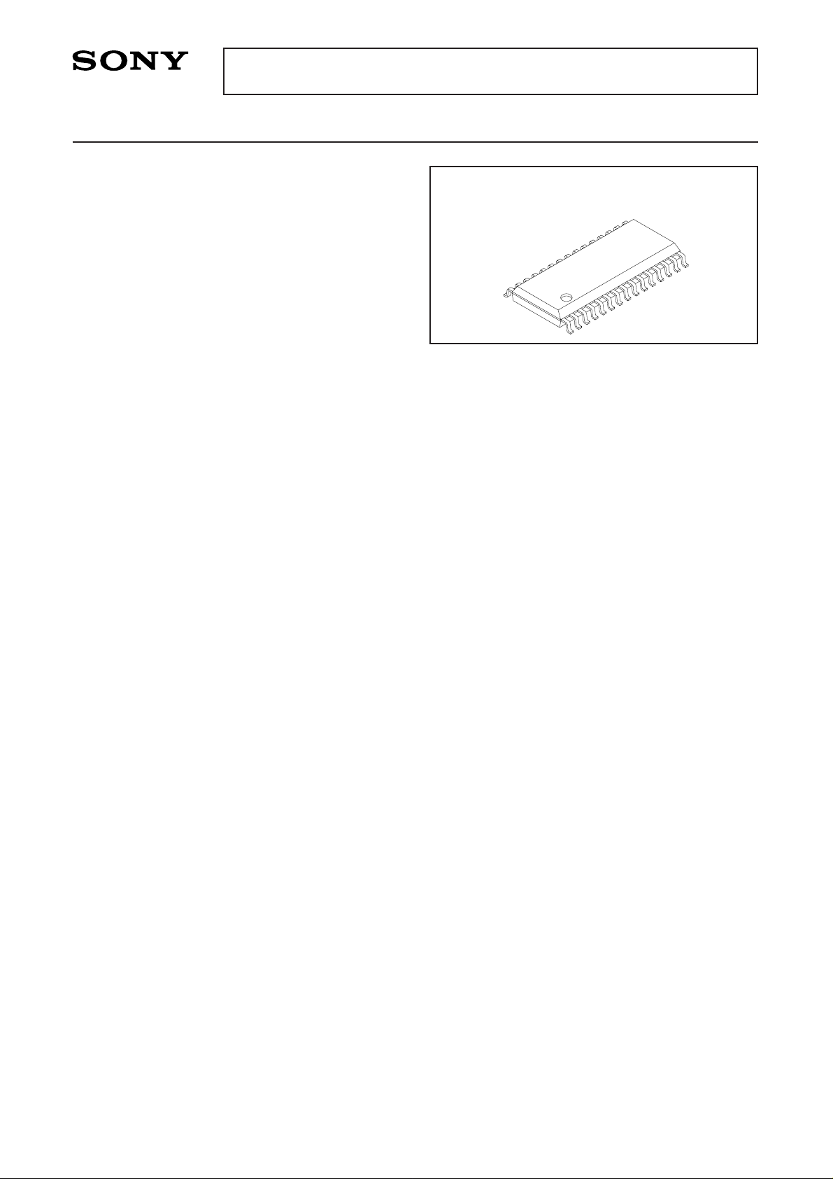
30 pin SOP (Plastic)
CXA3067M
Page 2
—2—
CXA3067M
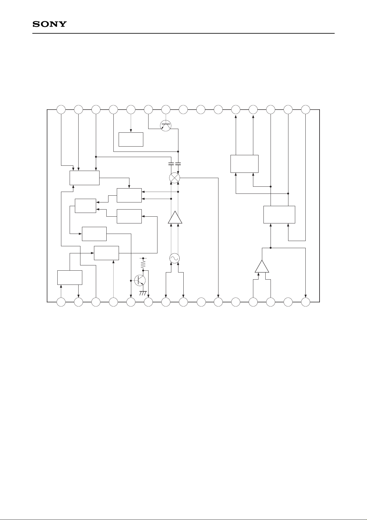
Pin configuration and Block diagram
8 91 2 10 11 12 13 14 15654 73
22 21 20 19 18 1727 26 23 1629 2830 25 24
FSET2
FSET3
REFSW
MIXIN
RFVCC
RFEM
RFIN
RFGND
IFGND
IFVCC
NOUT
POUT
LF2
LF1
DETIN
REFIN
XTAL
FSET1
RDSW
CPLF
VT
OSC1
OSC2
DGND
MIXOUT
DVCC
LIMIN
BYP
GND
LIMOUT
V.REG
FREQ
SELECT
PHASE
DET
MAIN
DIVIDER
REF
DIVIDER
CHARGE
PUMP
SCALER
REF
OSC
DATA
SHAPER
DET
MIX
OSC
LIM
Page 3
—3—
CXA3067M
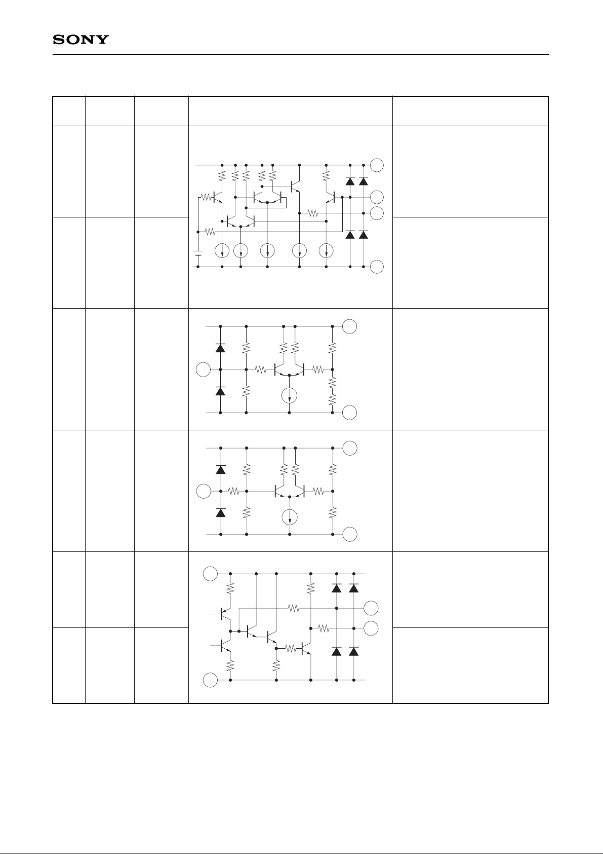
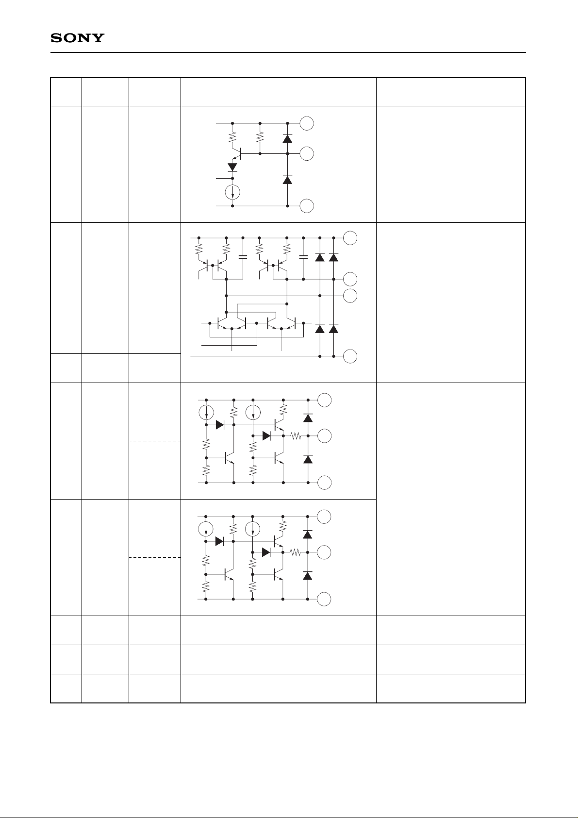
Pin Description and Equivalent Circuit
Pin
Symbol
Typical
Equivalent circuit Description
No. voltage (V)
1
2
3
4
5
6
REFIN
XTAL
FSET1
RDSW
CPLF
VT
3.4
4.0
2.5
(OPEN)
3.0
(OPEN)
2.0
0.3 to VCC
500
DVCC
1
2
11
9
DGND
3
11
9
20k
20k
DVCC
DGND
11
4
9
25k
20k
30k
DVCC
DGND
DVCC
5
6
10k
100
100
11
9
DGND
External clock input
and X’tal connection for
reference oscillator.
X’tal connection for
reference oscillator.
The pin for channel selection.
The condition of pin 3 has
3 states.
Connect to 5 V source for “Hi”
selection and connect to GND for
“Low” selection and leave open.
Reference frequency selection.
Connect to GND when reference
frequency is 14.3125 MHz or
14.31818 MHz and leave open
when reference frequency is
7.15625 MHz or 7.15909 MHz.
Charge pump output.
Connect to loop filter.
Connect to loop filter.
OSC tuning voltage output.
Page 4
—4—
CXA3067M
Pin
Symbol
Typical
Equivalent circuit Description
No. voltage (V)
7
8
9
10
11
12
13
14
15
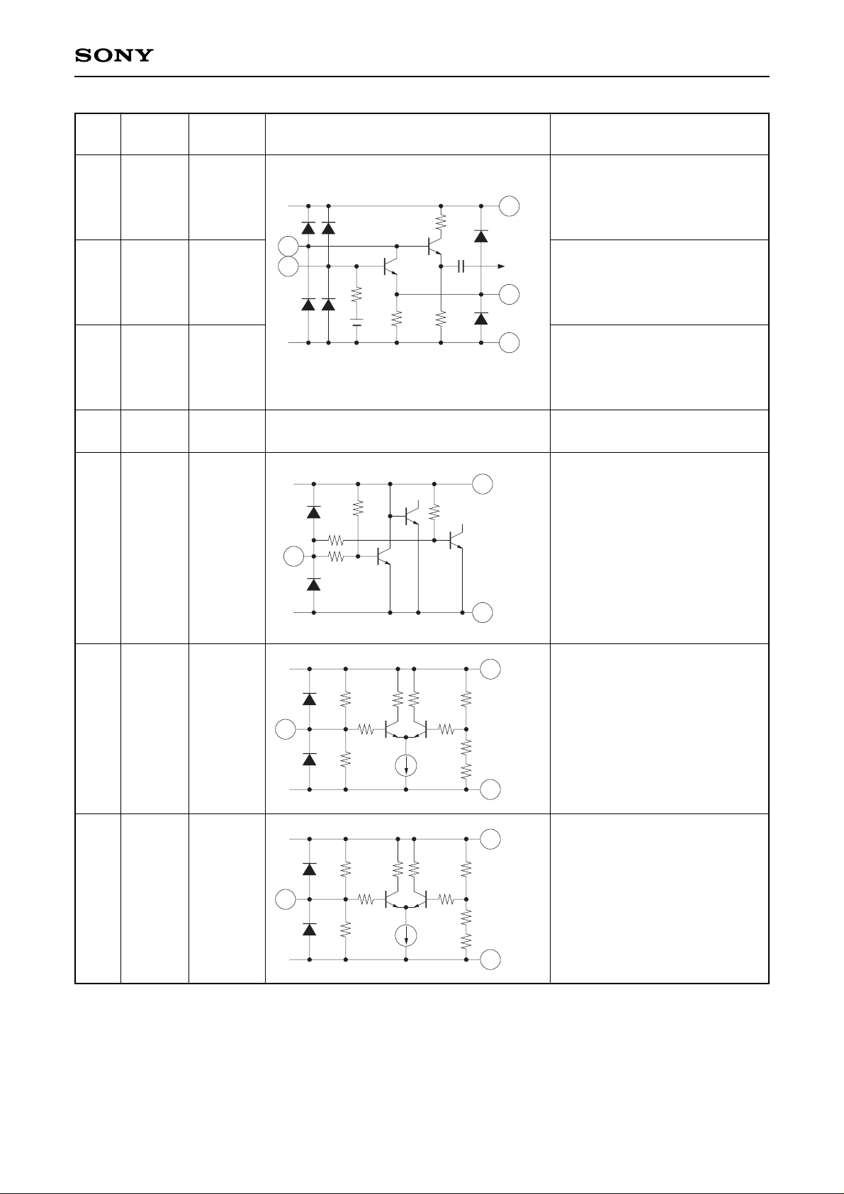
OSC1
OSC2
DGND
MIXOUT
DVCC
LIMIN
BYP
GND
LIMOUT
3.7
3.7
0
4.0
5
2.4
2.4
0
3.1
26
87
23
RFVCC
RFGND
700 700
3k
3k
26
10
23
330 330
RFVCC
RFGND
12
13
10k
330
10k
21
IFVCC
22
IFGND
IFVCC
21
15
IFGND
22
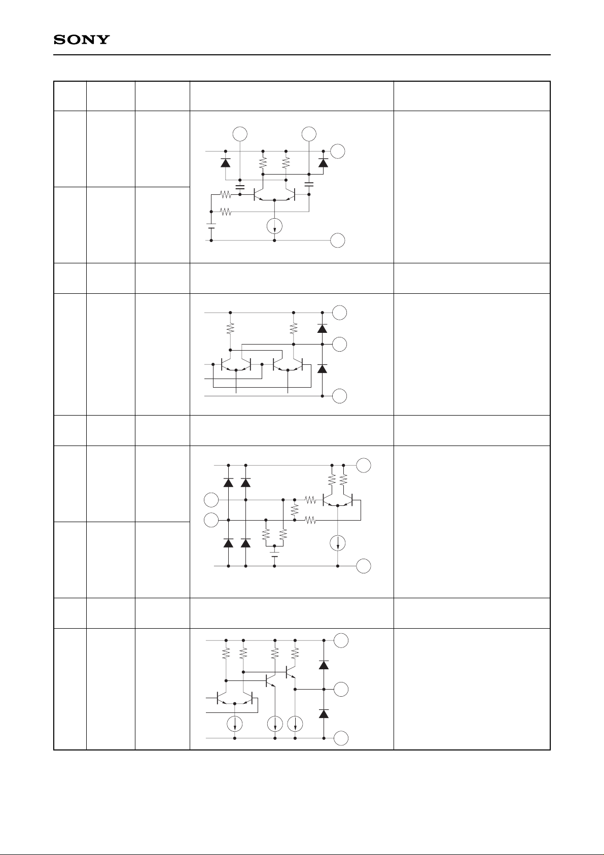
Oscillator.
PLL circuit GND.
Mixer output.
Output impedance is 330 Ω.
PLL circuit power supply.
Limiter input.
Input impedance is 330 Ω.
GND.
Limiter output.
Page 5
—5—
CXA3067M
Pin
Symbol
Typical
Equivalent circuit Description
No. voltage (V)
16
17
18
19
20
21
22
23
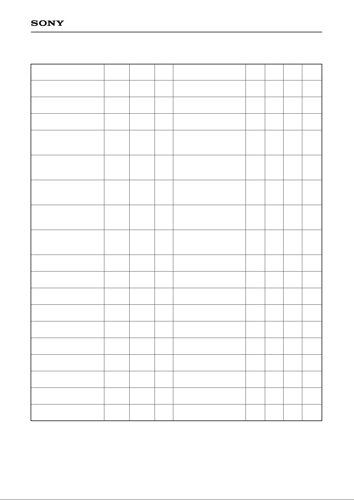
DETIN
LP1
LP2
POUT
NOUT
IFVCC
IFGND
RFGND
5.0
4.2
4.2
4.1
(Hi)
0.22
(Low)
4.1
(Hi)
0.22
(Low)
5.0
0
0
21
IFVCC
16
32k
22
IFGND
21
18
17
IFVCC
IFGND
12p 12p
22
21
19
IFVCC
IFGND
22
50
21
20
22
IFVCC
IFGND
50
Detector input.
Connect to a discriminator.
The capacitor is connected
between pins 17 and 18 for
the filter.
FSK data output.
Pins 19 and 20 are each
other reversal condition.
Power supply for limiter, detector,
data shaper circuit.
GND for limiter, detector,
data shaper circuit.
GND for RFamp, Mixer,
oscillator circuit.
Page 6
—6—
CXA3067M
Pin
Symbol
Typical
Equivalent circuit Description
No. voltage (V)
24
25
27
26
28
29
30
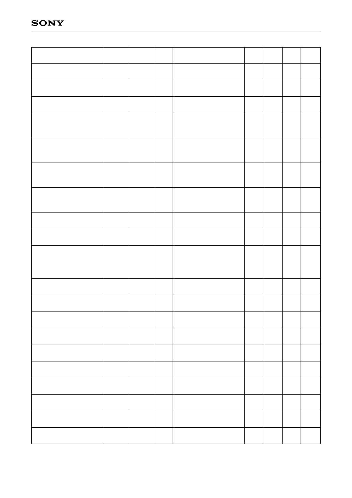
RFIN
RFEM
MIXIN
RFVCC
REFSW
FSET3
FSET2
1.9
1.1
5.0
5.0
0.7
(OPEN)
2.5
(OPEN)
2.5
(OPEN)
RFVCC
26
MIX
25
27
233
5k
24
RFGND
23
11
29
9
20k
20k
DVCC
DGND
28
DVCC
DGND
11
9
11
9
20k
20k
DVCC
DGND
30
RFamp input.
Gain adjustment.
Normally, by-pass capacitor is
connected at pin 25 to GND.
RFamp output and mixer input.
Power supply for RFamp, mixer,
oscillator circuit.
Reference frequency selection.
Decoupling capacitor is
connected at pin 28 to GND
when reference frequency is
7.15909 MHz or 14.31818 MHz
and pin 28 is connected to GND
directly when reference
frequency is 7.15625 MHz or
14.3125 MHz.
The pin of channel selection.
The condition of pin 29 has
3 states.
Connect to 5 V source for “Hi”
selection and connect to GND for
“Low” selection and leave open.
The pin of channel selection.
The condition of pin 30 has
3 states.
Connect to 5 V source for “Hi”
selection and connect to GND for
“Low” selection and leave open.
Page 7
—7—
CXA3067M
Electrical Characteristics
See Electrical Characteristics Test Circuit (VCC=5.0 V, Ta=+25 °C)
Item Symbol Pin No.
Circuit
Conditions Min. Typ. Max. Unit
No.
RFVCC
Current consumption
IFVCC
Current consumption
DVCC
Current consumption
Input sensitivity 1
Input sensitivity 2
Input level
Local OSC leakage
from RF input 1
Local OSC leakage
from RF input 2
RFamp bias current
RFamp voltage gain 1
RFamp voltage gain 2
RFamp voltage gain 3
RFamp input resistance
RFamp input capacitance
Mixer input resistance
Mixer input capacitance
Mixer voltage gain
RFamp+Mixer noise figure
RFI
CC
IFICC
DICC
Vi1
Vi2
Vil
LOleak1
LOleak2
Irf
Grf1
Grf2
Grf3
rπ (rf)
Cπ (rf)
rπ (mix)
Cπ (mix)
Gmix
NF
rfmix
26, 27
21
11
24
24
27
24
→27
24→27
24→27
24
24
27
27
27→10
24→10
RFV
CC
V1=5 V
IFV
CC
V2=5 V
DV
CC V4=1 V
V3=5 V
Measurement on RFIN pin
SW1 : ON
RF=53.35 M to 169.5 MHz
Measurement on RFIN pin
SW1 : ON
RF=221.95 M to 302 MHz
RFV
CC
V1=5 V
RF=53.35 M to 169.5 MHz
RF=221.95 M to 229.8 MHz
RF=302 MHz
I=4.8 mA, RF=100 MHz
Load Resistance=510 Ω
l=4.8 mA, RF=100 MHz
Load Resistance=510 Ω
RF=100 MHz
RF=100 MHz
RF=108.5 MHz→
IF=10.7 MHz
RF=108.5 MHz→
IF=10.7 MHz ∗
1
fMOD=10 kHz, fDEV=±75 kHz
Jitter is 1 % for f
MOD
50 Ω Termination
RF=53.35 M to 169.5 MHz
f
MOD=10 kHz, fDEV=±75 kHz
Jitter is 1 % for f
MOD
50 Ω Termination
RF=221.95 M to 302 MHz
f
MOD=10 kHz, fDEV=±75 kHz
Jitter is 1 % for f
MOD
50 Ω Termination
RF=53.35 M to 302 MHz
14 24 34 mA
3 6.7 10 mA
3.5 7 10 mA
–32 dBmV
–25 dBmV
+10 dBmV
–10 dBmV
+5 dBmV
3 4.8 7 mA
24 30 34 dB
22 25 28 dB
16 19 22 dB
670 Ω
4.7 pF
1.7 kΩ
5.7 pF
9 13 17 dB
7 dB
Note) 0 dBmV=1 mV, 0 dBµV=1 µV
∗
1
) Noise figure is uncorrected for image.
0 dBmV=60 dBµV
0 dBm=47 dBmV
1
1
1
2
2
2
2
2
1
3
3
3
4
5
Page 8
—8—
CXA3067M
Item Symbol Pin No.
Circuit
Conditions Min. Typ. Max. Unit
No.
Mixer output resistance
Limiter input resistance
Limiter voltage gain
FSK Data
output voltage “H”
FSK Data
output voltage “L”
FSK Data output rise time
FSK Data output fall time
Oscillation frequency
VT output voltage range
Charge pump current
REFCLOCK input level 1
REFCLOCK input level 2
REFOSC loop gain
FSET1/2/3 “Hi” level
input voltage
FSET1/2/3 “Low” level
input voltage
FSET1/2/3 “Hi” level
input current
FSET1/2/3 “Low” level
input current
RDSW “Low” level
input voltage
RDSW “Low” level
input current
REFSW “Low” level
input voltage
r
L (mix)
rπ (lim)
Glim
OUTH
OUTL
Tr
Tf
OSC
VT
Icp
CLK 1
CLK 2
Gref
FSETVH
FSETVL
FSETIH
FSETIL
RDVL
RDIL
REFVL
10
12
15
19, 20
19, 20
19, 20
19, 20
7, 8
6
5
1
1
1, 2
3, 29, 30
3, 29, 30
3, 29, 30
3, 29, 30
4
4
28
IF=10.7 MHz
IF=10.7 MHz
IF=10.7 MHz
Load Capacitance=2 pF
Load Resistance=10 kΩ,
f
MOD=10 kHz, fDEV=±75 kHz
Load Capacitance=2 pF
Load Resistance=10 kΩ,
f
MOD=10 kHz, fDEV=±75 kHz
Load Capacitance=2 pF
Load Resistance=10 kΩ,
f
MOD=10 kHz, fDEV=±75 kHz
Road Capacitance=2 pF
Road Resistance=10 kΩ,
f
MOD=10 kHz, fDEV=±75 kHz
Source current
→ SW2 : OFF
SW3 : OFF
Sink current → SW2 : ON
SW3 : ON
Sin wave input
Square wave input
Vin2=14 MHz
FSET “Hi”=V5=5 V
FSET “Low”=V5=0 V
RDSW “L”=V6=0 V
222 332 442 Ω
222 332 442 Ω
70 dB
3.8 4.1 V
0.22 0.6 V
12 30 nsec
12 30 nsec
40 315 MHz
0.3 2.5 V
CC V
±25 ±50 ±75 µA
0.3 0.4 3.0 Vp-p
0.3 0.4 3.0 Vp-p
30 dB
3.8 V
CC V
0 0.4 V
120 250 380 µA
–380 –250 –120 µA
0 0.4 V
–122 –83 –43 µA
0 0.4 V
6
2
2
2
2
7
3
1
1
1
1
1
1
1
Page 9
—9—
CXA3067M
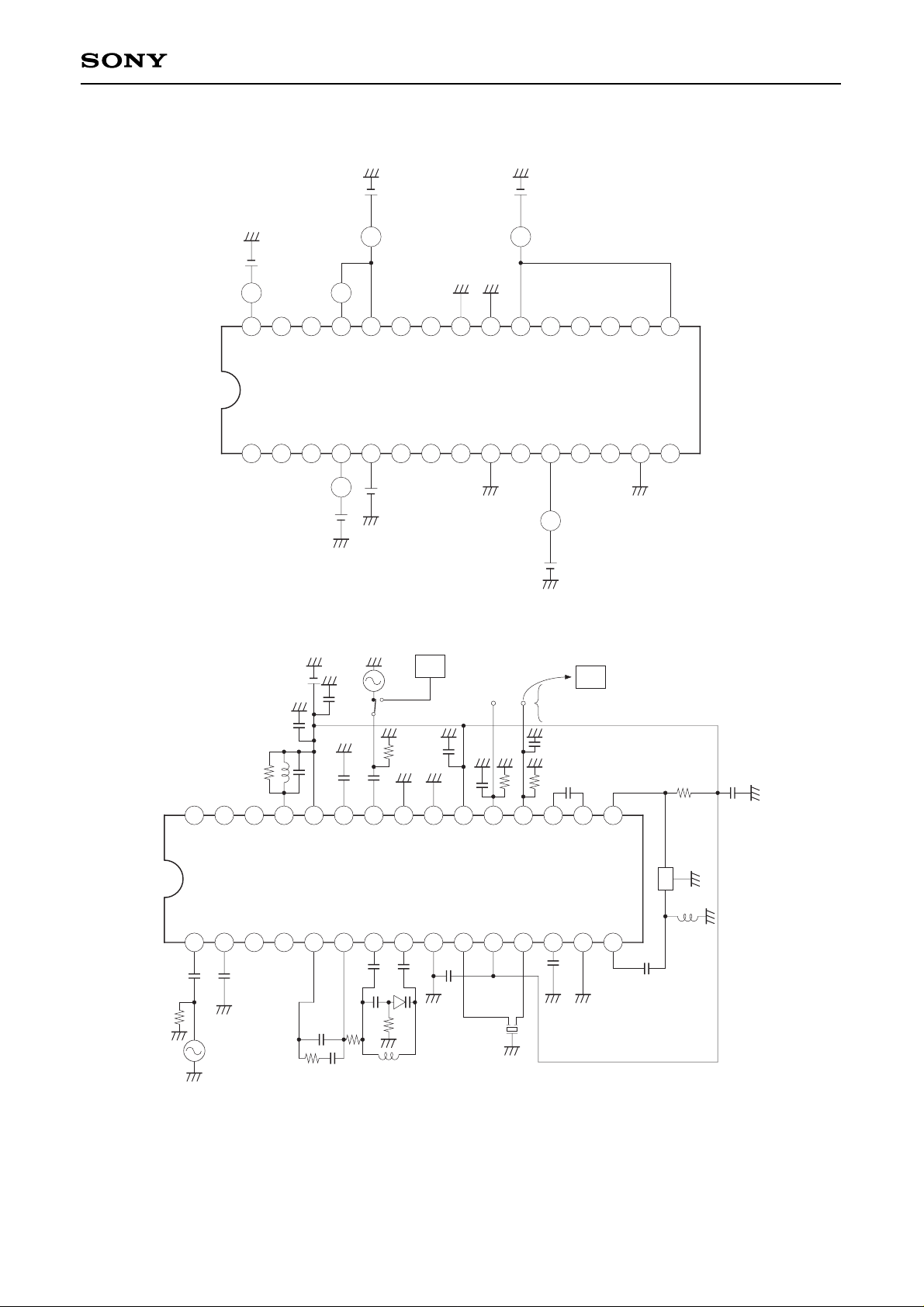
Electrical Characteristics Test Circuit
A A
A
AA
V5
22 21 20 19 18 1727 26 23 1629 2830 25 24
A
V6
8 91 2
10 11 12 13 14 15
654 73
V1
5V
V2
5V
V4
1V
V3
5V
REFIN
XTAL
FSET1
RDSW
CPLF
VT
OSC1
OSC2
DGND
MIXOUT
DVCC
LIMIN
BYP
GND
LIMOUT
FSET2
FSET3
REFSW
MIXIN
RFVCC
RFEM
RFIN
RFGND
IFVCC
NOUT
POUT
LF2
LF1
DETIN
IFGND
8 91 2
10 11 12 13 14 15
654 73
22 21 20 19 18 1727 26 23 1629 2830 25 24
5V
10n
4.7µ
Vin
SW1
Spectrum
analyzer
Passive
probe
Oscilloscope
10.8P
10M
10 : 1
SELECTION
1n
10n
51
10n
NEG
POS
10k
10k
680p
330
10n
51
10n
10n
SELECTION
fref
51p
51p
51k
1T362
10n
10n
MIXOUT
REFIN
XTAL
FSET1
RDSW
CPLF
VT
OSC1
OSC2
DGND
DVCC
LIMIN
BYP
GND
LIMOUT
FSET2
FSET3
REFSW
MIXIN
RFVCC
RFEM
RFIN
RFGND
IFGND
IFVCC
NOUT
POUT
LF2
LF1
DETIN
51k
56p
2p
2p
5.6µ
Measurement circuit 1
Measurement circuit 2
Measurement : Input sensitivity, local osc leakage,
FSK DATA output voltage,
rise time, fall time
Measurement : Current consumption
Page 10

—10—
CXA3067M
Vin1
Vout1
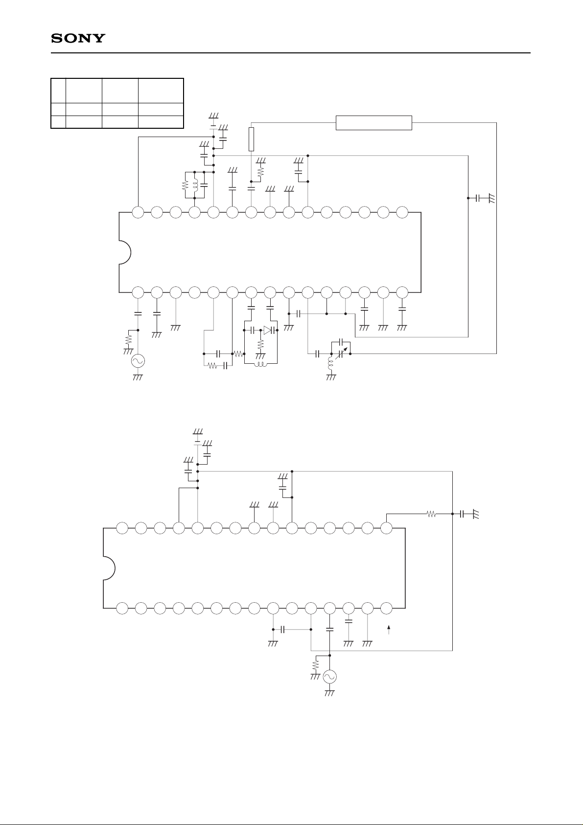
GV=Vout1/Vin1 (RFamp voltage gain)
GV=Vout2/Vin2 (REFOSC loop gain)
5V
4.7µ
10n
1n
10n
51
51
10n
Vin2
Vout2
10n
FSET2
FSET3
REFSW
MIXIN
RFVCC
RFEM
RFIN
RFGND
IFGND
IFVCC
NOUT
POUT
LF2
LF1
DETIN
REFIN
XTAL
FSET1
RDSW
CPLF
VT
OSC1
OSC2
DGND
MIXOUT
DVCC
LIMIN
BYP
GND
LIMOUT
22 21 20 19 18 1727 26 23 1629 2830 25 24
5V
8 91 2
10 11 12 13 14 15
654 73
Vout1
8 91 2
10 11 12 13 14 15
654 73
22 21 20 19 18 1727 26 23 1629 2830 25 24
5V
4.7µ
10n
510
L1
120p
1n
10n
51
10n
Vin
G
V=Vout2/Vout1
51
10n
10n
fref
3.3n
27k 30n
51k
51p
51p
100p
51k
1T362
L2
Vout2
10n
330
10n
REFIN
XTAL
FSET1
RDSW
CPLF
VT
OSC1
OSC2
DGND
MIXOUT
DVCC
LIMIN
BYP
GND
LIMOUT
FSET2
FSET3
REFSW
MIXIN
RFVCC
RFEM
RFIN
RFGND
IFGND
IFVCC
POUT
LF2
LF1
DETIN
NOUT
10n
Measurement circuit 3
Measurement circuit 4
L1
L2
Wire
diameter
0.5
0.5
Coil
diameter
3 φ
3.8 φ
Number of
windings
1.5 T
6.5 T
Measurement : RFamp voltage gain
:REFOSC loop gain
Measurement : Mixer voltage gain
Page 11
—11—
CXA3067M
22 21 20 19 18 1727 26 23 1629 2830 25 24
8 91 2
10 11 12 13 14 15
654 73
5V
10n
510
L1
120p
1n
10n
51
10n
Noise Source
Noise Figure meter
10n
51
10n
10n
fref
3.3n
27k 30n
51k
51p
51p
100p
51k
1T362
L2
10n
10n
110p
40p
2.2µ
10n
10n
FSET2
FSET3
REFSW
MIXIN
RFVCC
RFEM
RFIN
RFGND
IFGND
IFVCC
NOUT
POUT
LF2
LF1
DETIN
4.7µ
REFIN
XTAL
FSET1
RDSW
VT
OSC1
OSC2
DGND
MIXOUT
DVCC
LIMIN
BYP
GND
LIMOUT
CPLF
22 21 20 19 18 1727 26 23 1629 2830 25 24
8 91 2
10 11 12 13 14 15
654 73
5V
10n
4.7µ
GV=Vout/Vin
10n
330
10n
10n
Vin
Vout
10n
10n
51
REFSW
FSET2
FSET3
MIXIN
RFVCC
RFEM
RFIN
RFGND
IFGND
IFVCC
NOUT
POUT
LF2
LF1
DETIN
REFIN
XTAL
FSET1
RDSW
CPLF
VT
OSC1
OSC2
DGND
MIXOUT
DVCC
LIMIN
BYP
GND
LIMOUT
Measurement circuit 5
Measurement circuit 6
L1
L2
Wire
diameter
0.5
0.5
Coil
diameter
3 φ
3.8 φ
Number of
windings
1.5 T
6.5 T
Measurement : RFamp +Mixer NF
Measurement : Limiter voltage gain
Page 12

—12—
CXA3067M
A
22 21 20 19 18 1727 26 23 1629 2830 25 24
8 91 2
10 11 12 13 14 15
654 73
V1
5V
10n
4.7µ
1n
10n
SW2
V4
4V
fref
14MHz
51
10n
V5
2.5V
V6
0V
V7
10V
SW3
51k
51p
51p
10n
51k
1T362
10n
FSET2
FSET3
REFSW
MIXIN
RFVCC
RFEM
RFIN
RFGND
IFGND
IFVCC
NOUT
POUT
LF2
LF1
DETIN
REFIN
XTAL
FSET1
RDSW
CPLF
VT
OSC1
OSC2
DGND
MIXOUT
DVCC
LIMIN
BYP
GND
LIMOUT
100P
L2
Measurement circuit 7
Measurement : Charge pump current
L2
Wire
diameter
0.5
Coil
diameter
3.8 φ
Number of
windings
6.5 T
Page 13

—13—
CXA3067M
Function Explanation
The CXA3067M is an integrated circuit designed for CATV wide band FSK receiver. This monolithic IC is
composed of local oscillator, double balanced mixer, limiter, FM detector, data shaper and PLL circuit in a
single chip.
The function of each other section is described below.
1. RFamp circuit
This circuit amplifies RF signal, and RF signal is input to pin 24 (RFIN).
Since pin 27 is an open collector, connect power supply through a coil which composes tune circuit or a
choke coil or a resistor.
RF signal is selected a desired frequency by this tune circuit.
The desired frequency is input to mixer circuit through coupling capacitor.
2. Mixer circuit
This is a double-balanced mixer having small leakage of local signal.
The RF signal is converted to IF signal by the signal supplied from oscillator.
The output impedance is approximately 330 Ω.
Normally, connect a ceramic filter to 10 pin (MIXOUT).
3. Local oscillator circuit
The balanced oscillator circuit with pins 7 and 8 (OSC1, OSC2).
Connect an LC resonance circuit comprising a varicap diode to pins 7 and 8.
4. PLL circuit
The PLL circuit fixes the local oscillator frequency to desired frequency.
It consists of the main divider, reference divider, phase comparator, charge pump, reference oscillator.
As stated in the accompanying document, desired frequency (channel) can be selected through the
combination of the conditions of pins 1, 29 and 30 (FSET 1; 2; 3).
As stated in the accompanying document, reference frequency can be selected through the combination
the conditions of pin 3 (RDSW) and pin 28 (REFSW).
5. Limiter circuit
This circuit amplifies the mixer IF output through ceramic filter.
For quadrature FM detection, this circuit amplifies IF signal by necessary level.
The input impedance is approximately 330 Ω.
6. Detector circuit
For quadrature FM detection, the phase of limiter output (pin 15) is shifted 90° by discriminator as the
output is input to pin 16.
7. Data shaper
This circuit output performs the waveform shaping of the demodulated FSK signal and outputs the resulting
signal as a rectangular wave.
Page 14
—14—
CXA3067M
Description of PLL Block
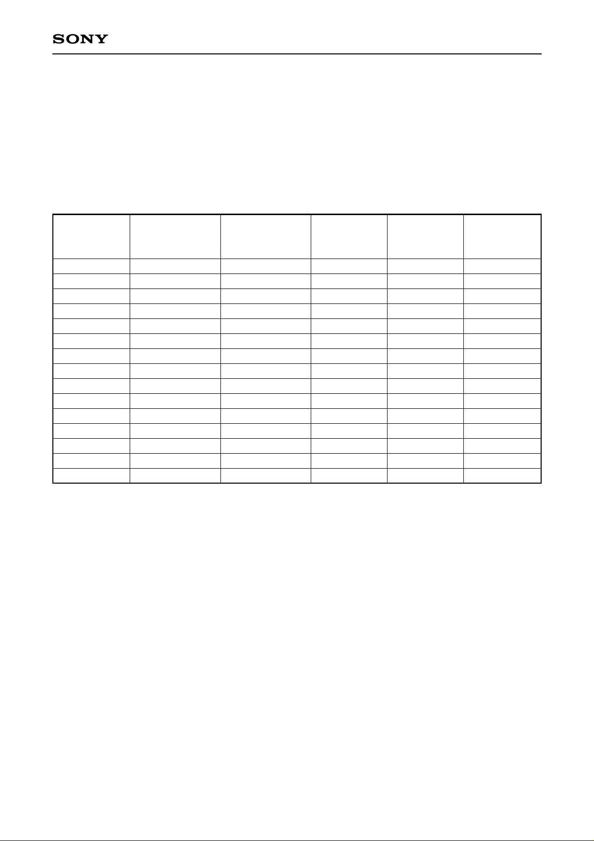
1. The followings “channel No.” can be selected through the combination of the conditions of pins 1, 29 and 30
(FSET 1; 2; 3).
FSET conditions have 3 states (OPEN, Hi, Low).
Channel Selection
Channel No.
1
2
3
4
5
6
7
8
9
10
11
12
13
14
15
Local
OSC frequency
[MHz]
42.65
83.70
98.20
100.00
108.20
117.20
117.80
119.20
133.40
139.20
168.70
180.20
211.25
219.10
312.70
Receiving
frequency
[MHz]
53.55
73.00
87.50
89.30
97.50
106.50
128.50
108.50
122.70
128.50
158.00
169.50
221.95
229.80
302.00
FSET 1
OPEN
L
H
OPEN
L
H
OPEN
L
H
OPEN
L
H
OPEN
L
H
FSET 2
OPEN
OPEN
OPEN
L
L
L
H
H
H
OPEN
OPEN
OPEN
L
L
L
FSET 3
OPEN
OPEN
OPEN
OPEN
OPEN
OPEN
OPEN
OPEN
OPEN
L
L
L
L
L
L
Note) OPEN : No connect
L : Connect to GND
H : Connect to VCC
Page 15
—15—
CXA3067M
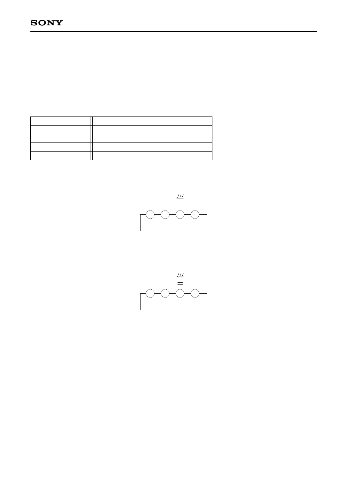
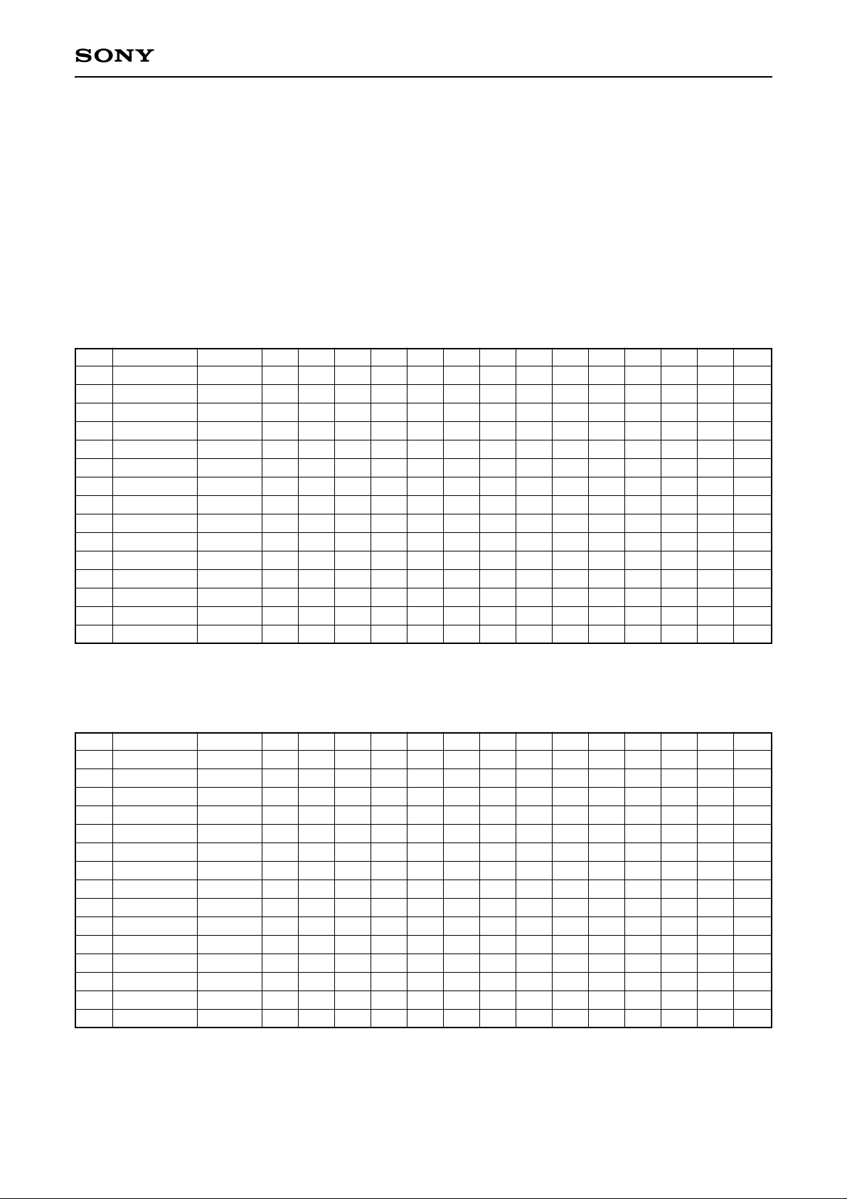
2. The followings Reference frequency can be selected through the combination the conditions of pin 3
(RDSW) and pin 28 (REFSW).
When the pin 28 is connected to GND directly, the pin 28 is state of DCGND.
When the pin 28 is connected to GND through decoupling capacitor, the pin 28 is state of ACGND.
Reference Frequency selection
f (ref)
7.15625 MHz
7.15909 MHz
14.3125 MHz
14.31818 MHz
RDSW
OPEN
OPEN
GND
GND
REFSW
DCGND
ACGND
DCGND
ACGND
∗1
∗2
∗1
∗2
Note∗1) Connect to GND directly.
Note∗2) Connect to GND through decoupling capacitor
REFSW
30 29 28 27
REFSW
30 29 28 27
Page 16
—16—
CXA3067M
3. The comparison frequency is 25.021853 kHz at reference frequency 7.15625 MHz/14.3125 MHz, and
25.031783 kHz at reference frequency 7.15909 MHz/14.31818 MHz.
The frequency division ratio of the reference divider is 286.
The frequency division ratio of the scaler is 1 or 2;
When the reference frequency is 7.15625 MHz/7.15909 MHz, the frequency division ratio of the scaler is 1.
When the reference frequency is 14.3125 MHz/14.31818 MHz, the frequency division ratio of the scaler is 2.
Reference frequency=7.15625 MHz
The comparison frequency=7.15625/286=25.021853 kHz
Reference frequency=7.15909 MHz
The comparison frequency=7.15909/286=25.031783 kHz
Ch
1
2
3
4
5
6
7
8
9
10
11
12
13
14
15
fOSC [MHz]
42.65
83.7
98.2
100
108.2
117.2
117.8
119.2
133.4
139.2
168.7
180.2
211.25
219.1
312.7
Divider
1705
3345
3925
3997
4324
4684
4708
4764
5331
5563
6742
7202
8443
8756
12497
8192
0
0
0
0
0
0
0
0
0
0
0
0
1
1
1
4096
0
0
0
0
1
1
1
1
1
1
1
1
0
0
1
2048
0
1
1
1
0
0
0
0
0
0
1
1
0
0
0
1024
1
1
1
1
0
0
0
0
1
1
0
1
0
0
0
512
1
0
1
1
0
1
1
1
0
0
1
0
0
1
0
256
0
1
1
1
0
0
0
0
0
1
0
0
0
0
0
128
1
0
0
1
1
0
0
1
1
1
0
0
1
0
1
64
0
0
1
0
1
1
1
0
1
0
1
0
1
0
1
32
1
0
0
0
1
0
1
0
0
1
0
1
1
1
0
16
0
1
1
1
0
0
0
1
1
1
1
0
1
1
1
8
1
0
0
1
0
1
0
1
0
1
0
0
1
0
0
4
0
0
1
1
1
1
1
1
0
0
1
0
0
1
0
2
0
0
0
0
0
0
0
0
1
1
1
1
1
0
0
1
1
1
1
1
0
0
0
0
1
1
0
0
1
0
1
Ch
1
2
3
4
5
6
7
8
9
10
11
12
13
14
15
fOSC [MHz]
42.65
83.7
98.2
100
108.2
117.2
117.8
119.2
133.4
139.2
168.7
180.2
211.25
219.1
312.7
Divider
1704
3344
3923
3995
4323
4682
4706
4762
5329
5561
6739
7199
8439
8753
12492
8192
0
0
0
0
0
0
0
0
0
0
0
0
1
1
1
4096
0
0
0
0
1
1
1
1
1
1
1
1
0
0
1
2048
0
1
1
1
0
0
0
0
0
0
1
1
0
0
0
1024
1
1
1
1
0
0
0
0
1
1
0
1
0
0
0
512
1
0
1
1
0
1
1
1
0
0
1
0
0
1
0
256
0
1
1
1
0
0
0
0
0
1
0
0
0
0
0
128
1
0
0
1
1
0
0
1
1
1
0
0
1
0
1
64
0
0
1
0
1
1
1
0
1
0
1
0
1
0
1
32
1
0
0
0
1
0
1
0
0
1
0
0
1
1
0
16
0
1
1
1
0
0
0
1
1
1
1
1
1
1
0
8
1
0
0
1
0
1
0
1
0
1
0
1
0
0
1
4
0
0
0
0
0
0
0
0
0
0
0
1
1
0
1
2
0
0
1
1
1
1
1
1
0
0
1
1
1
0
0
1
0
0
1
1
1
0
0
0
1
1
1
1
1
1
0
Page 17

—17—
CXA3067M
Notes on Application
Take care of the followings because the CXA3067M has limiter voltage gain of approximately 67 dB and uses
high frequency.
1) Separate the input pattern from the output pattern as far as possible and makes wiring short.
2) Ground the decoupling capacitor as close to pin 13 as possible.
Take care of the followings in order to reduce the jitter.
1) Insert the capacitor as close to pin 17 and 18 as possible.
2) Ground the by-pass capacitor as close to IFVCC to supply pin 16 as possible.
Take care of the following, for the purpose of the isolation of local oscillator resonance circuit and X’tal (RFF
CLOCK).
1) Separate the patterns connected pin 1 and pin 2 from the local oscillator resonance circuit.
Take care of the following, in order to reduce the phase noise.
1) Connect the loop filter as close to pins 5 and 6 as possible.
Take care of the following, in order to prevent the parasitic oscillation.
1) Connect the local oscillator resonance circuit as close to pins 7 and 8 as possible.
And compact the local oscillator resonance circuit.
The tuning voltage at the local oscillator resonance circuit.
The output voltage at pin 6 is 0.3 V to VCC.
When the oscillation frequency is the desired frequency, please the output voltage at pin 6 should be been 2.5 V.
Please decide the component value of loop filter by each system.
DVCC
5
6
10k
100
100
11
9
DGND
Page 18
—18—
CXA3067M
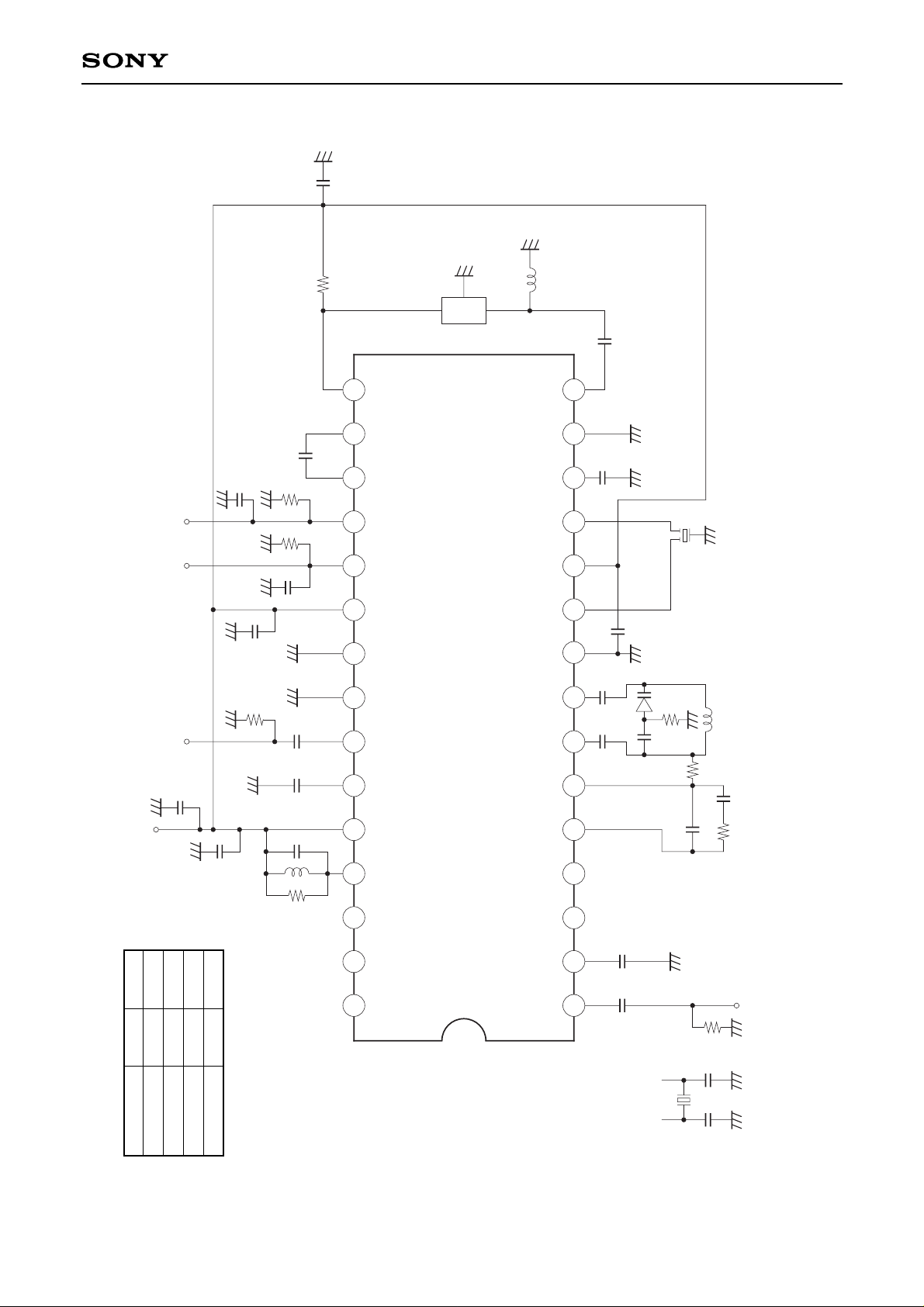
Application
56p
5.6µ
8 91 2 10 11 12 13 14 15654 73
22 21 20 19 18 1727 26 23 1629 2830 25 24
CXA3067M
REFIN
XTAL
FSET1
RDSW
CPLF
VT
OSC1
OSC2
DGND
MIXOUT
DVCC
LIMIN
BYP
GND
LIMOUT
SELECTION
TUNE CIRCUIT OF RFAMP
VCC (+5V)
RF INPUT FSK DATA OUT FSK DATA OUT
1n
10n
51
10n
2p
10k
10k
NEG
POS
2p
680p
330
10n
FIXED DISCRIMINATOR
10.7MHz
14MHz
X’tal
REF CLOCK INPUT
SELECTION
LOOP FILTER
15p
15p
51
51k
LOCAL OSCILLATOR
51p
51p
51k
1T362
10n
10.7MHz
CERAFIL
10n
Please refer to another sheets with following circuits.
1) Tuned circuit of RFamp
2) Local osc resonance circuit
3) Loop filter
4.7µ
10n
10n
10n
FSET3
REFSW
MIXIN
RFVCC
RFEM
RFIN
RFGND
IFGND
IFVCC
NOUT
POUT
LF2
LF1
DETIN
FSET2
Application circuits shown are typical examples illustrating the operation of the devices. Sony cannot assume responsibility for
any problems arising out of the use of these circuits or for any infringement of third party patent and other right due to same.
fref
7.15625 MHz
7.15909 MHz
14.3125 MHz
14.31818 MHz
RDSW
OPEN
OPEN
GND
GND
REFSW
DCGND
ACGND
DCGND
ACGND
Page 19
—19—
CXA3067M
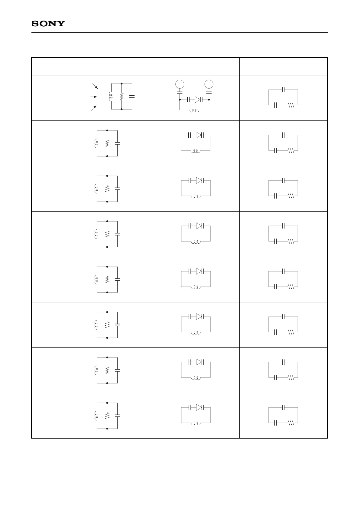
The component value of the tune circuit, local oscillator resonance circuit and loop filter.
Channel Tune circuit Local oscillator
Loop filter
No. of RFamp resonance circuit
1
2
3
4
5
6
7
8
510
330p
0.5
2.5T
3φ
Wire
diameter
Number of
windings
Coil
diameter
510
180p
0.5
2.5T
3φ
510
120p
0.5
2.5T
3φ
510
120p
0.5
2.5T
3φ
510
82p
0.5
2.5T
3φ
510
150p
0.5
1.5T
3φ
510
100p
0.5
1.5T
3φ
510
120p
0.5
1.5T
3φ
51p
7 8
51p
1T362
1n
0.5
20.5T
5φ
82p
0.5 11.5T 3.8φ
100p
0.5 8.5T 3.8φ
100p
0.5 8.5T 3.8φ
100p
0.5 8.5T 3.8φ
100p
0.5 6.5T 3.8φ
100p
0.5 6.5T 3.8φ
100p
0.5 6.5T 3.8φ
3.3n
39n 24k
3.3n
30n 27k
3.3n
30n 27k
3.3n
30n 27k
3.3n
30n 27k
3.3n
30n 27k
3.3n
30n 27k
3.3n
30n 27k
Page 20
—20—
CXA3067M
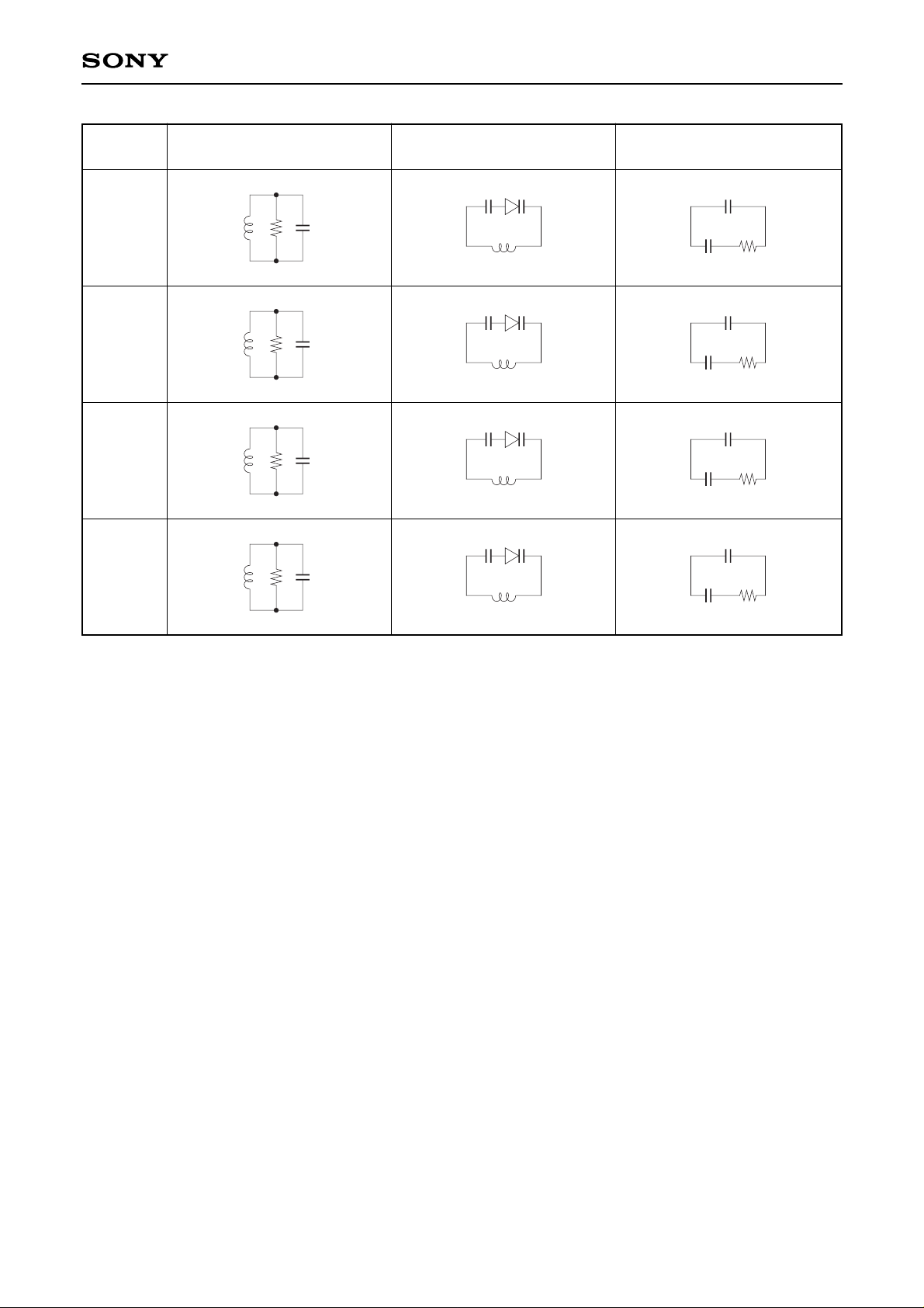
Channel Tune circuit Local oscillator
Loop filter
No. of RFamp resonance circuit
9
10
11
12
510
100p
0.5
1.5T
3φ
510
100p
0.5
1.5T
3φ
510
62p
0.5
1.5T
3φ
510
56p
0.5
1.5T
3φ
100p
0.5 5.5T 3.8φ
100p
0.5 5.5T 3.8φ
100p
0.5 3.5T 3.8φ
62p
0.5 3.5T 3.8φ
3.3n
30n 27k
3.3n
30n 27k
3.3n
30n 27k
3.3n
30n 30k
Page 21

—21—
CXA3067M
RFamp gain (dB)
Frequency response RF amp voltage gain
Reception Frequency (MHz)
Limiter gain (dB)
Frequency response limiter voltage gain
Intermediate Frequency (MHz)
Leakage level (dBm)
Local oscillation leakage at RFIN pin
Local oscillation frequency (MHz)
LP1 Output Level (V)
S curve response
Intermediate Frequency (MHz)
Current consumption (mA)
Supply voltage vs. Current consumtion
Supply voltage (V)
30
25
15
10
5
0
RF BLOCK
PLL BLOCK
IF BLOCK
4.6 4.7 4.8 4.9 5 5.1 5.2 5.3 5.4
32
30
28
26
24
22
20
18
10 100 300
90
80
70
60
50
40
30
20
1 10 100
–50
–55
–60
–65
–75
–80
1 100 1000
4.32
4.31
4.3
4.29
4.28
4.27
4.26
10.6 10.65 10.7 10.75 10.8
20
–70
Page 22
—22—
CXA3067M
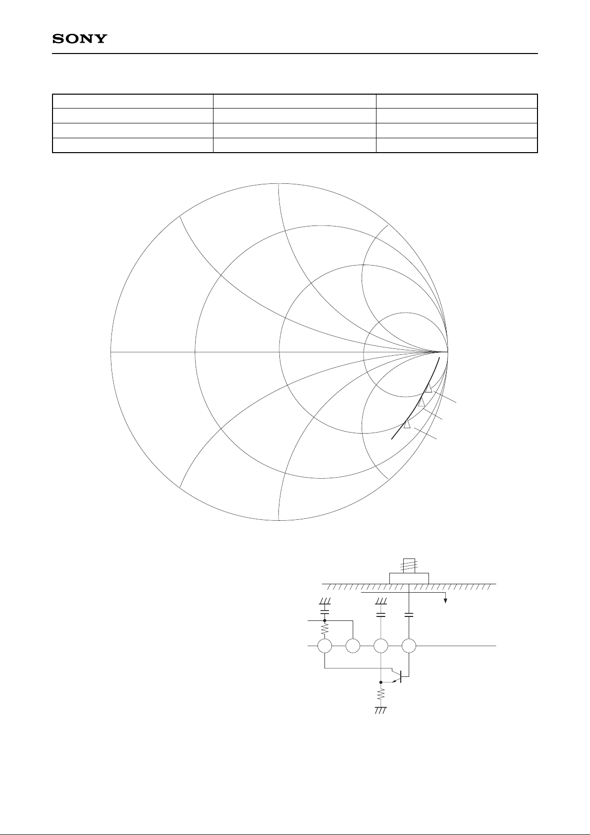
RFIN Input Impedance (Resistance, Capacitance)
j100
j50
j25
0
–j25
–j50
–j100
50MHz
100MHz
200MHz
24252627
SMA
Connector
PCB
Calibration plane
IC
CXA3067M
S11
1nF1nF
VCC
5V
1nF
510Ω
Reception frequency
50 MHz
100 MHz
200 MHz
Resistance
890 Ω
670 Ω
510 Ω
Capacitance
5.2 pF
4.7 pF
4.4 pF
Page 23
—23—
CXA3067M
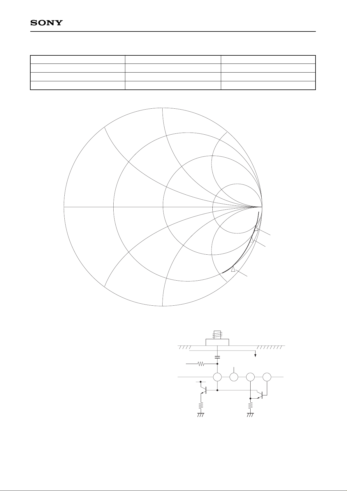
MIXIN Input Impedance (Resistance, Capacitance)
j100
j50
j25
0
–j25
–j50
–j100
50MHz
100MHz
200MHz
24252627
SMA
Connector
PCB
Calibration plane
IC
CXA3067M
S11
VCC
1nF
11kΩ
60V
RFVCC
Reception frequency
50 MHz
100 MHz
200 MHz
Resistance
2.1 kΩ
1.7 kΩ
900 Ω
Capacitance
5.7 pF
5.7 pF
6.1 pF
Page 24
0.5 ± 0.2
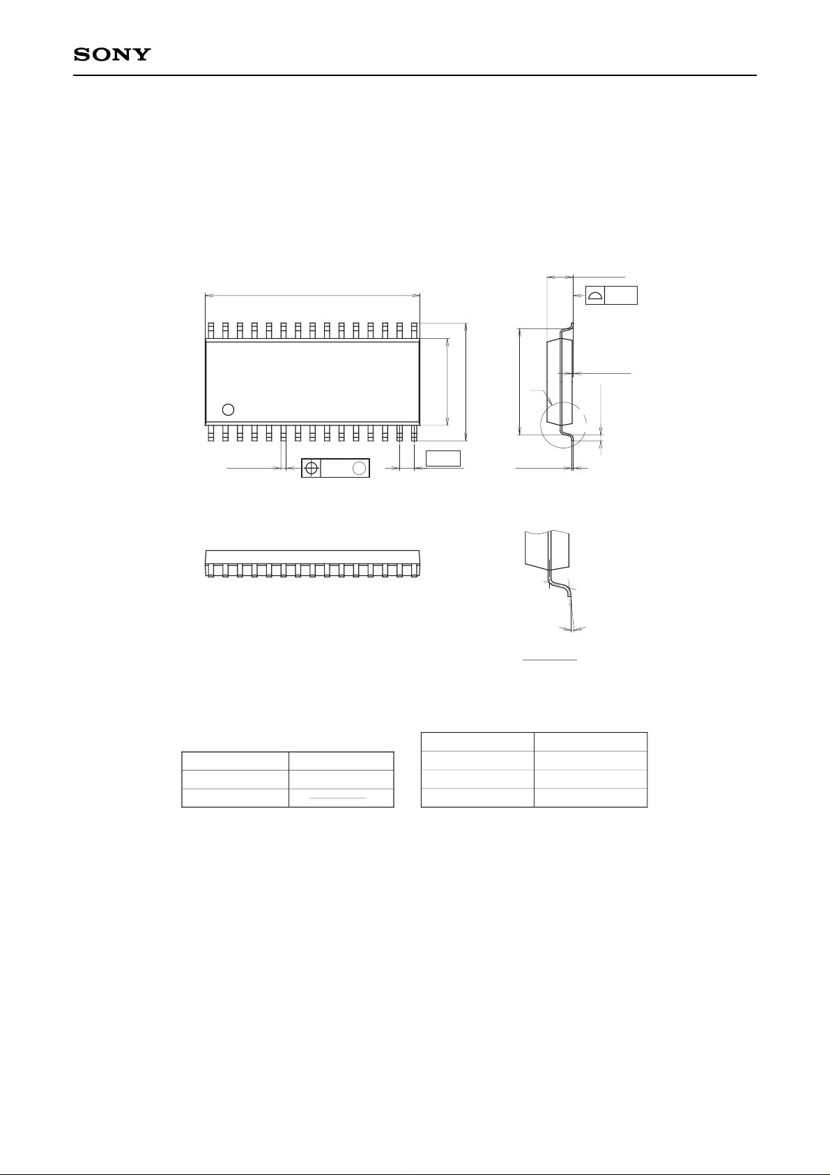
Package Outline Unit : mm
30
+ 0.4
18.8 – 0.1
30PIN SOP(PLASTIC)
16
+ 0.3
7.6 – 0.1
10.3 ± 0.4
CXA3067M
+ 0.4
2.3 – 0.15
0.1
+ 0.2
0.1 – 0.05
A
(9.3)
1
0.45 ± 0.1
SONY CODE
EIAJ CODE
JEDEC CODE
0.2
SOP-30P-L03
SOP030-P-0375
15
M
1.27
+ 0.1
0.2 – 0.05
0° to 10°
DETAILA
PACKAGE STRUCTURE
PACKAGE MATERIAL
LEAD TREATMENT
LEAD MATERIAL
PACKAGE MASS
EPOXY RESIN
SOLDER PLATING
COPPER ALLOY
0.7g
—24—
 Loading...