

Page 1

Headphone Stereos
Description
This is a bipolar IC designed for headphone stereos.
It provides functions such as automatic volume limiter
control, bass boost, standby, headphone driver and
others.
Features
• Low quiescent current (3.2mA at 2.4V Vcc )
• Thermal shutdown circuitry at 120°C
• Headphone driver (30mW at 2.4V Vcc for 16Ω load)
• Bass boost function (9dB)
• Standby function
• Wide operating voltage (1.8 to 5V)
• Automatic volume limiter control (100mVrms)
• Uses SOP 16 pin package
Application
Headphone Stereos
Structure
Bipolar silicon monolithic IC
Absolute Maximum Ratings (Ta = 25°C)
• Supply voltage VCC 7V
•Operating temperature Topr –20 to +75 °C
• Storage temperature Tstg –65 to +150 °C
• Allowable power dissipation PD 500 mW
Operating Conditions
Supply voltage VCC 1.8 to 5 V
– 1 –
E98830A91-PS
Sony reserves the right to change products and specifications without prior notice. This information does not convey any license by
any implication or otherwise under any patents or other right. Application circuits shown, if any, are typical examples illustrating the
operation of the devices. Sony cannot assume responsibility for any problems arising out of the use of these circuits.
CXA2566M
16 pin SOP (Plastic)
Page 2
– 2 –
CXA2566M
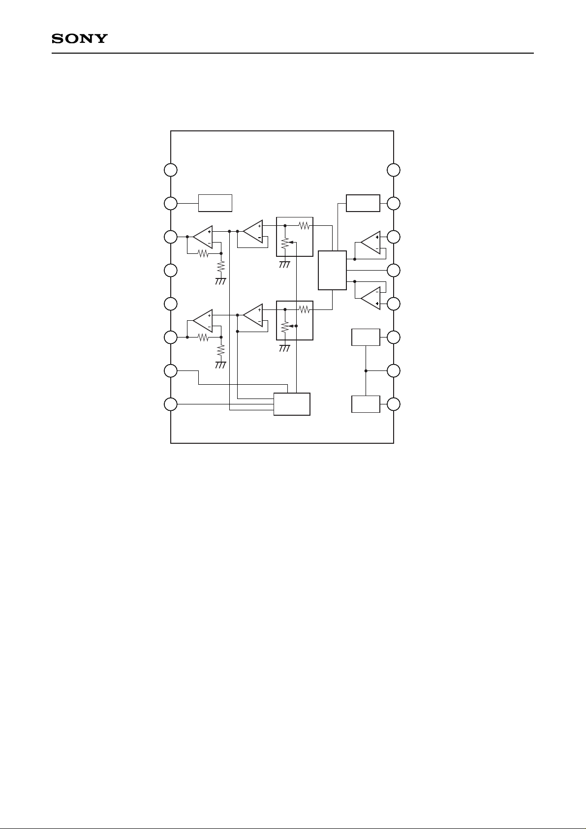
Block Diagram and Pin Configuration
1
2
3
4
5
6
7
8
9
10
11
12
13
14
15
16
GND
Standby
Pwr_1
PV
CC
PGND
Pwr_2
Det
AVLS
V
CC
Bass
Left
C
Right
Vref
RF_In
RF_Out
Standby Bass sw
Vref
Ripple
Bass
Boost
Detector
Page 3
– 3 –
CXA2566M
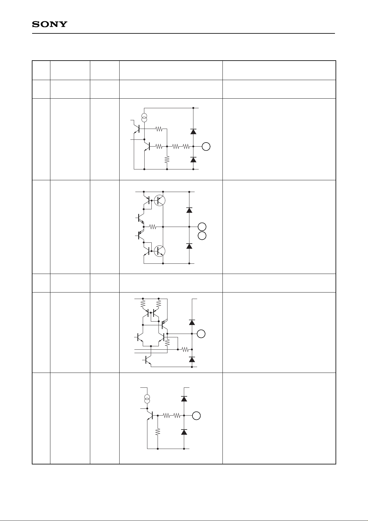
Pin Description
Standby switch
H: Operate
L: Standby
Pin
No.
Symbol
Equivalent circuit
Description
1
5
GND
PGND
Pre-amp ground
Power amp ground
2
Standby
Pin
Voltage
0
0
4
16
PVCC
VCC
Power amp supply
Pre-amp supply
0
0
1
2
VCC
GND
100k
2k2k20k 124
Left channel output
Right channel output
3
6
Pwr_1
Pwr_2
1.2
1.2
3
6
VCC
GND
3k
v
v
Detector output
7
Det
< 1
VCC
GND
80k
10k
vvv
10k
124
7
VCC
GND
100k
20k 124
8
AVLS switch
H: AVLS on
L: AVLS off
8
AVLS 0
Page 4
– 4 –
CXA2566M
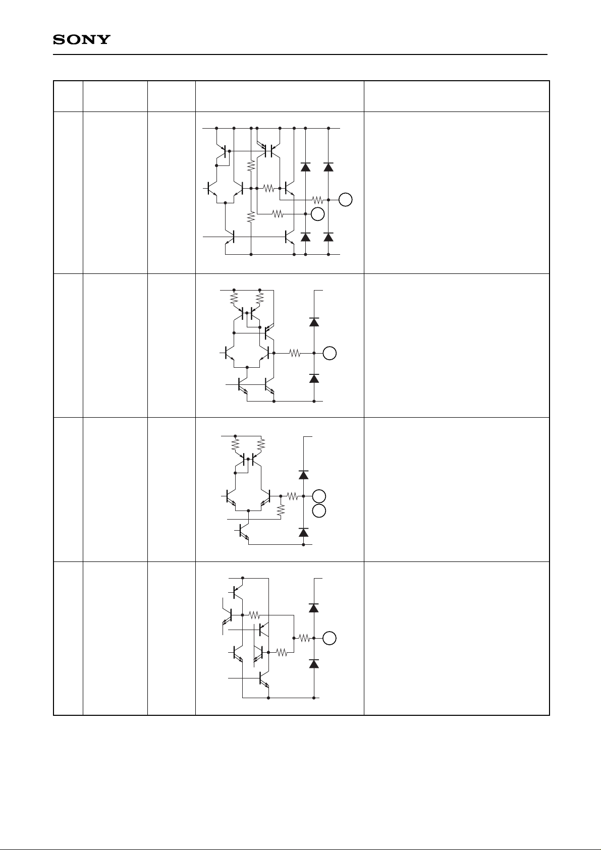
Right channel input
Left channel input
12
14
Right
Left
1.2
vv
12
14
VCC
GND
25k
10k 10k
124
Low pass filter output
13
C
1.2
v
v
VCC
GND
32k
124
32k
13
Pin
No.
Symbol
Equivalent circuit
Description
Pin
Voltage
Ripple filter output
9
10
RF_Out
RF_In
2.2
2.2
v vv
VCC
GND
368k
32k
124
10
9
100k
124
Voltage reference output
11
Vref
1.2
vvv
11
VCC
GND
10k 10k
124
Page 5
– 5 –
CXA2566M
Pin
No.
Symbol
Equivalent circuit
Description
Pin
Voltage
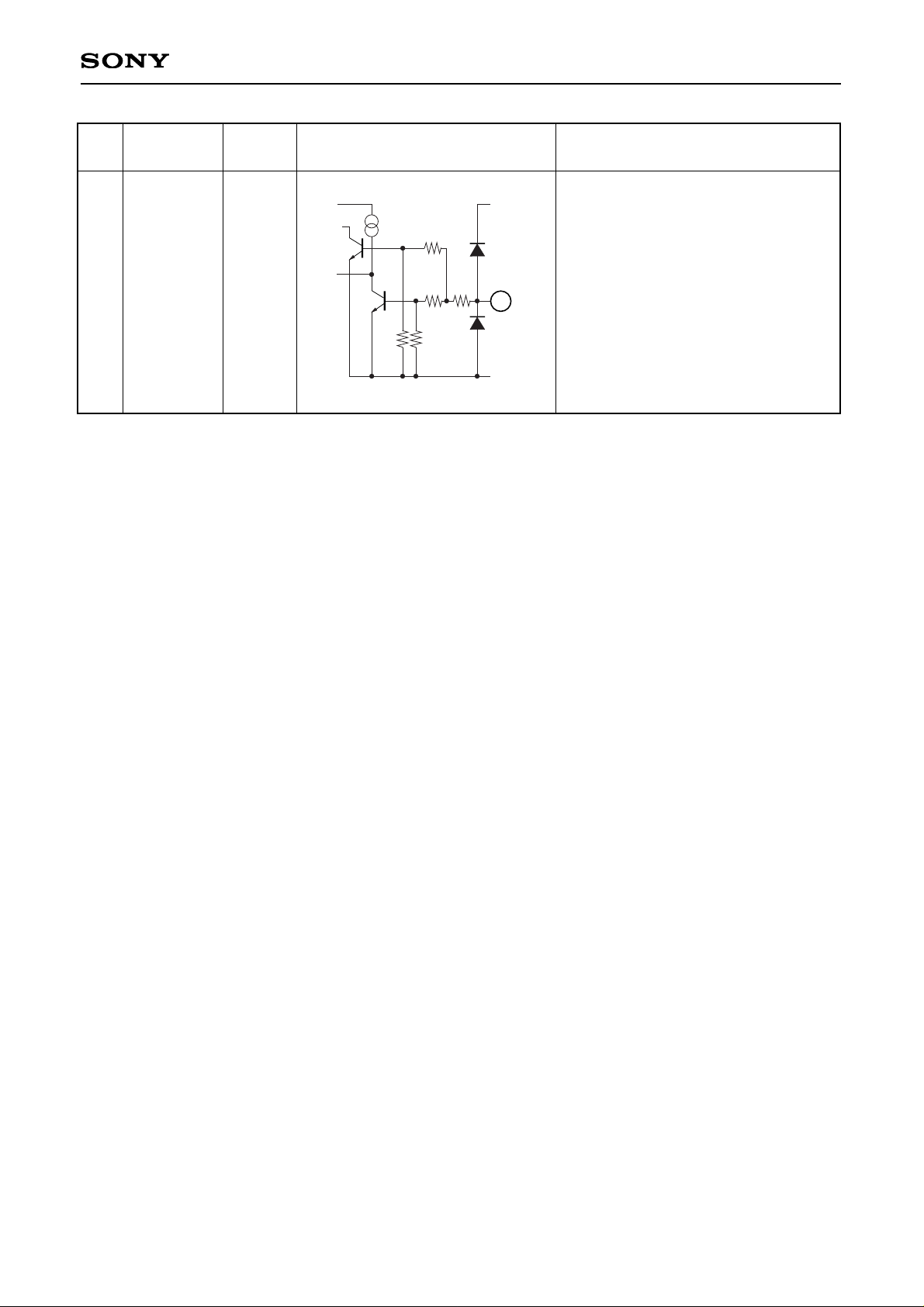
Bass switch
H: Bass on
L: Bass off
15
Bass
1
VCC
GND
20k
100k
100k
124
20k
15
Page 6
– 6 –
CXA2566M
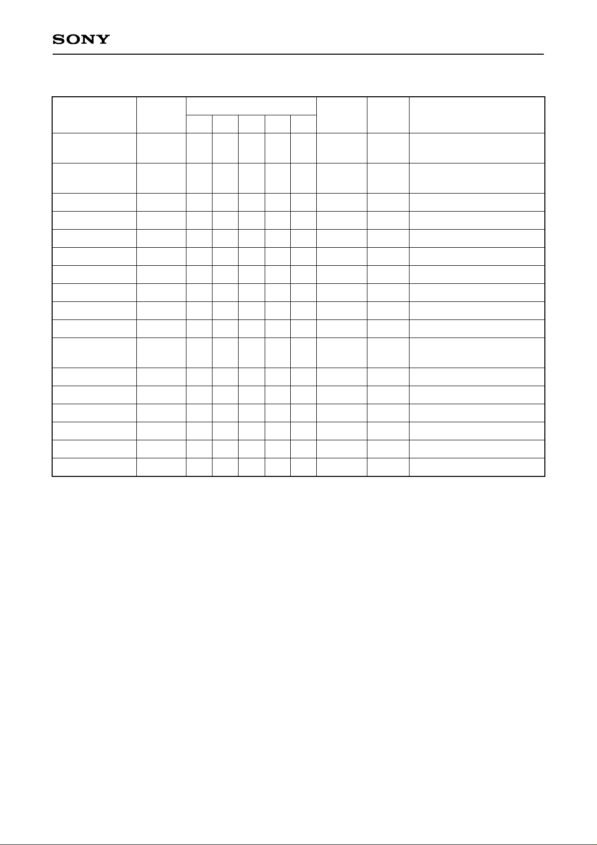
Electrical Characteristics
Items
Current
consumption 1
Current
consumption 2
Voltage gain 1
Voltage gain 2
AVLS output 1
AVLS output 2
Maximum Power
Distortion factor
Noise output
Ripple Rejection
Channel
Separation
Standby off
Standby switch
Bass on
Bass switch
AVLS on
AVLS switch
Symbols
Sw Condition
Sw1
Off
Off
Off
Off
On
On
Off
Off
Off
Off
Off
Off
Off
Off
Off
On
On
ICC1
ICC2
AV1
AV2
VAVLS1
VAVLS2
PO1
THD
Vno
RR
CS
Vstandby
Istandby
VBass
IBass
Vavls
Iavls
Sw2
On
Off
Off
Off
Off
Off
Off
Off
Off
Off
Off
Off
Off
Off
Off
Off
Off
Sw3
Off
Off
Off
On
Off
Off
Off
Off
Off
Off
Off
Off
Off
On
On
Off
Off
Sw4
Off
Off
On
On
On
On
On
On
Off
Off
On/
off
Off
Off
Off
Off
Off
Off
Sw5
Off
Off
On
On
On
On
On
On
Off
Off
Off/
on
Off
Off
Off
Off
Off
Off
Vin
–20dBm
50mVp-p
250mVp-p
Vrr
–20dBm
Measurement conditions
BB on, ∆Av at 100Hz and 1kHz
THD = 10%
VO = 0.3Vrms
Rg = 0, A-weight
VO = –10dBv
Vstandby = 1V
VBass = 1V
Vavls = 1V
Page 7
– 7 –
CXA2566M
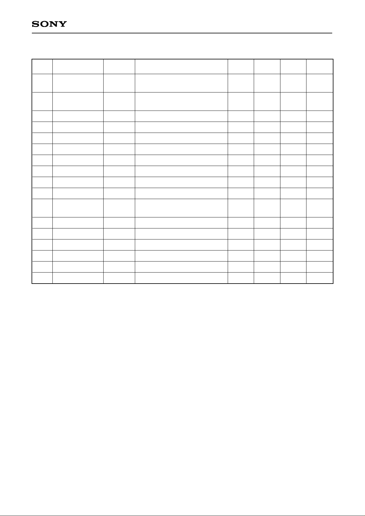
(Unless otherwise specified. Ta = 25°C, VC = 2.4V, RL = 16Ω, f = 1kHz, standby off, AVLS off, BB off)
Items
Current
consumption 1
Current
consumption 2
Voltage gain 1
Voltage gain 2
AVLS output 1
AVLS output 2
Maximum Power
Distortion factor
Noise output
Ripple Rejection
Channel
Separation
Standby off
Standby switch
Bass on
Bass switch
AVLS on
AVLS switch
No.
1
2
3
4
5
6
7
8
9
10
11
12
13
14
15
16
17
Symbols
ICC1
ICC2
AV1
AV2
VAVLS1
VAVLS2
PO1
THD
Vno
RR
∗1
CS
∗1
Vstandby
Istandby
VBass
IBass
Vavls
Iavls
Min.
—
—
11
8
86
86
15
—
—
36
–46
Typ.
18
3.2
11.78
9.22
103
104
30
0.13
–84
61
–50
1
15
1
30
1
15
Measurement conditions
Standby on
Vin = –20dBm
BB on, ∆Av at 100Hz and 1kHz
AVLS on, Vin = 50mVp-p
AVLS on, Vin = 250mVp-p
VCC = 2.4V, THD = 10%
VO = 0.3Vrms
Rg = 0
fR = 1kMz, VRR = –20dBm
VO = –10dBv
Vstandby = 1V
VBass = 1V
Vavls = 1V
Max.
23
5
12
10
116
116
—
0.3
–80
—
—
Units
µA
mA
dB
dB
mVrms
mVrms
mW
%
dBm
dB
dB
V
µA
V
µA
V
µA
∗1
Values are measured with respect to input source.
Page 8
– 8 –
CXA2566M
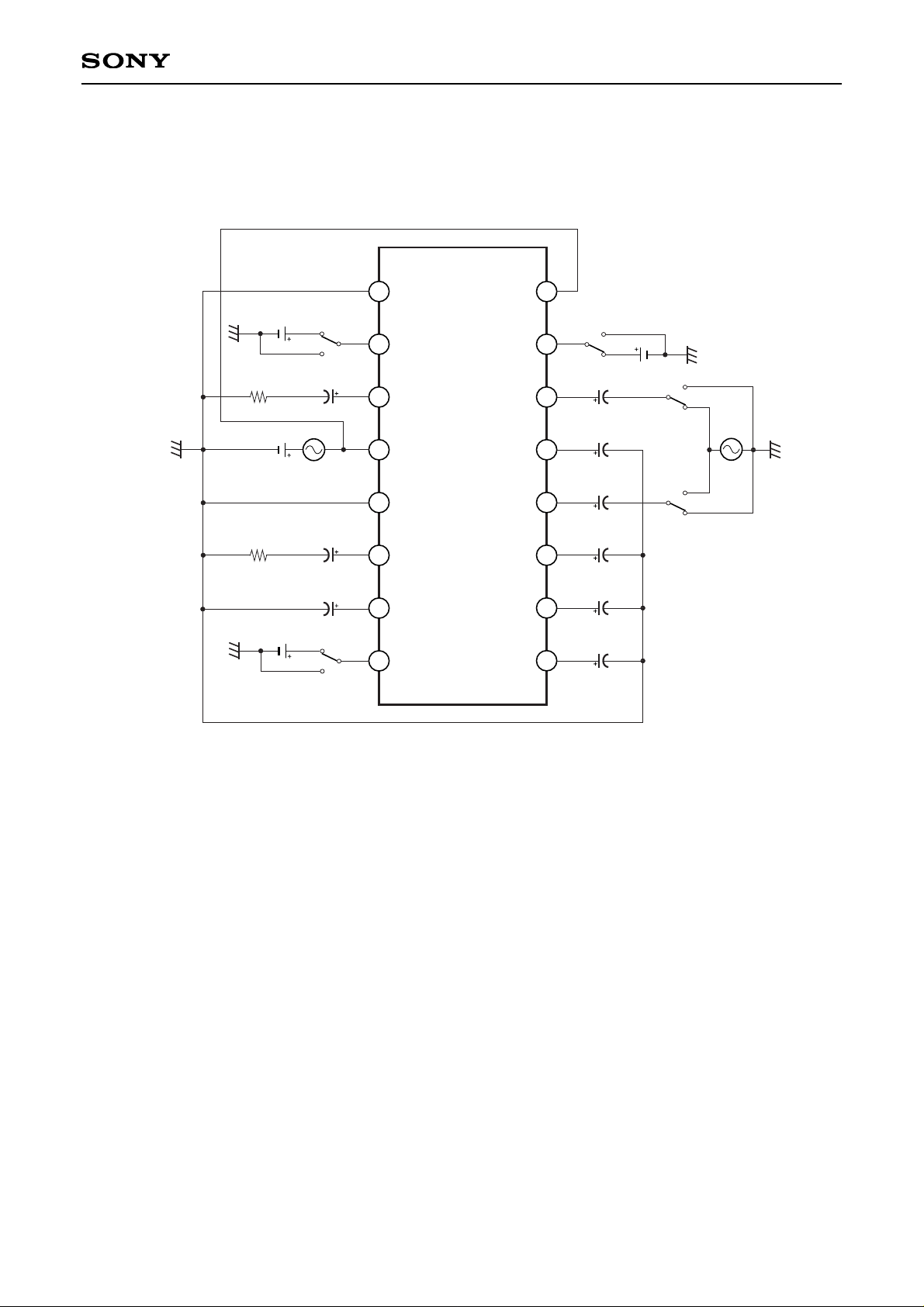
Electrical Characteristics Measurement Circuit
1
2
3
4
5
6
7
8
9
10
11
12
13
14
15
16
GND
Standby
Pwr1
PV
CC
PGND
Pwr2
AVLS
Det
V
CC
Bass
Left
C
Right
Vref
RF_In
C5 10µ
C6 10µ
C7 1µ
C9 1µ
V3
OFF
ON
C8 0.1µ
C4 1µ
RF_Out
C1 10µ
S3
OFF
V1
ON
OFF
VCC Vrr
S1
V2
OFF
ON
S2
ON
S5
Vin
ON
OFF
S4
C2 220µR1 16
C3 220 µR2 16
Page 9

– 9 –
CXA2566M
Description of Operation
1) Det Pin (Pin 7)
This is the external pin for the detector during AVLS mode. The attack time is determined by the internal
charging buffer and the external capacitor. The recovery time is determined by both the 80k impedance inside
the IC and the external capacitor.
2) RF_Out (Pin 9) / RF_In (Pin 10)
These are the two external pin for the power supply's ripple filter. It provides a regulated 0.92 × Vcc to the
internal circuits. The rejection ratio is determined by the resistors inside the IC and the two external capacitors.
VCC
Regulated
V
CC
RF_OutRF_In
32k
100k
368k
10 9
3) C Pin (Pin 13)
Out
Left
Out
Right
32k
32k
Left
Right
32k
32k
65k
21k
32k
C
32k
32k
32k
32k
32k
13
The bass boost circuitry is designed to provide a 9dB
gain at 100Hz for C = 0.1µF.
The cut off frequency is determined by:
fcutoff =
1
2π × 16k × C
Page 10
– 10 –
CXA2566M
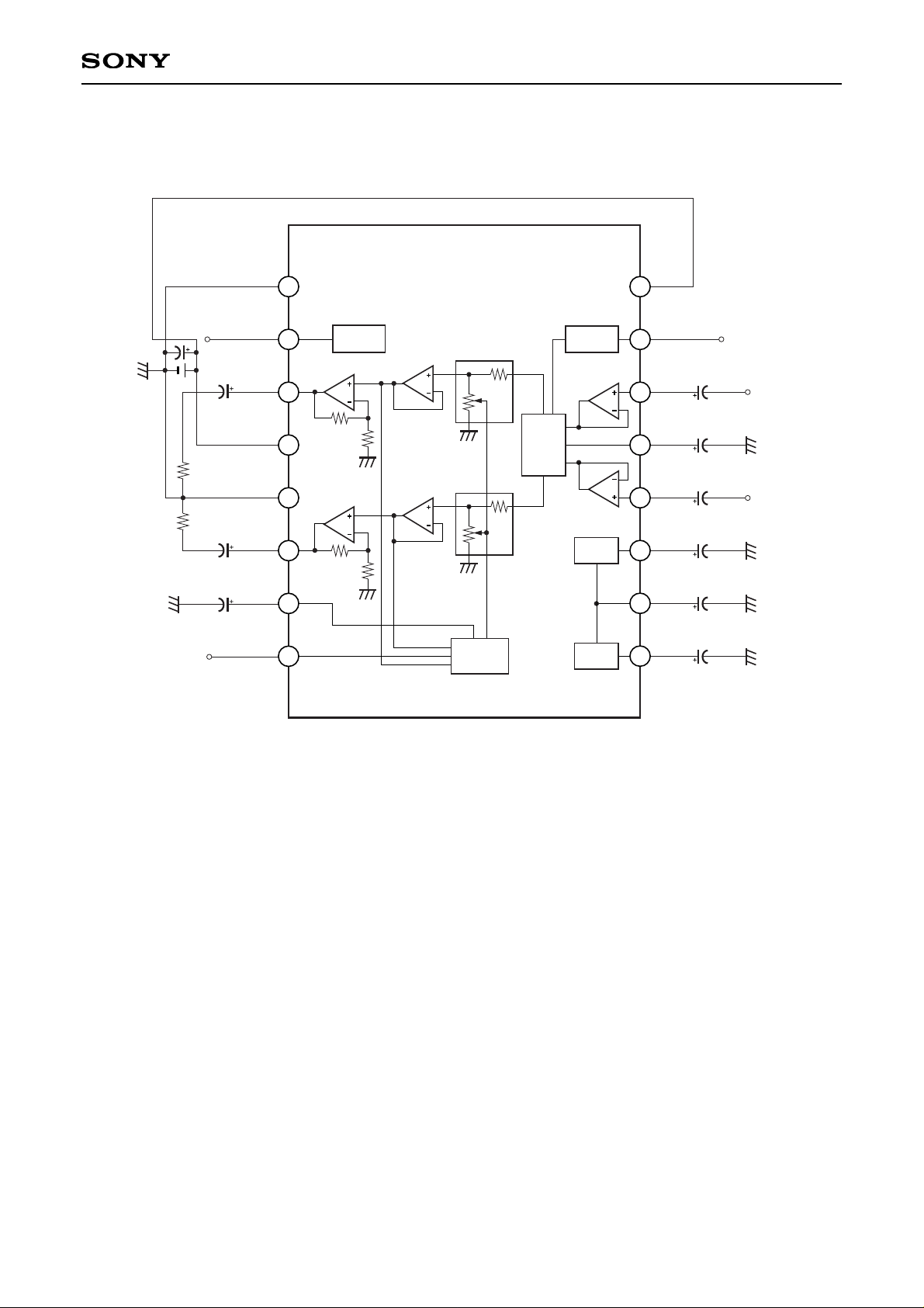
Application Circuit
2
GND
Standby
Pwr_1
PV
CC
PGND
Pwr_2
AVLS
Det
V
CC
Bass
1: Bass On
0: Bass Off
1: AVLS On
0: AVLS Off
1: Standby Off
0: Standby On
Left
C
Right
Vref
RF_In
RF_Out
Standby Bass sw
1µ
0.1µ
1µ
10µ
10µ
1µ
Vref
Ripple
Bass
Boost
Detector
10µ
220µ
16
16
220µ
14
15
9
10
11
12
13
2.4V
220µ
3
4
5
6
7
8
16
1
Application circuits shown are typical examples illustrating the operation of the devices. Sony cannot assume responsibility for
any problems arising out of the use of these circuits or for any infringement of third party patent and other right due to same.
Page 11
– 11 –
CXA2566M
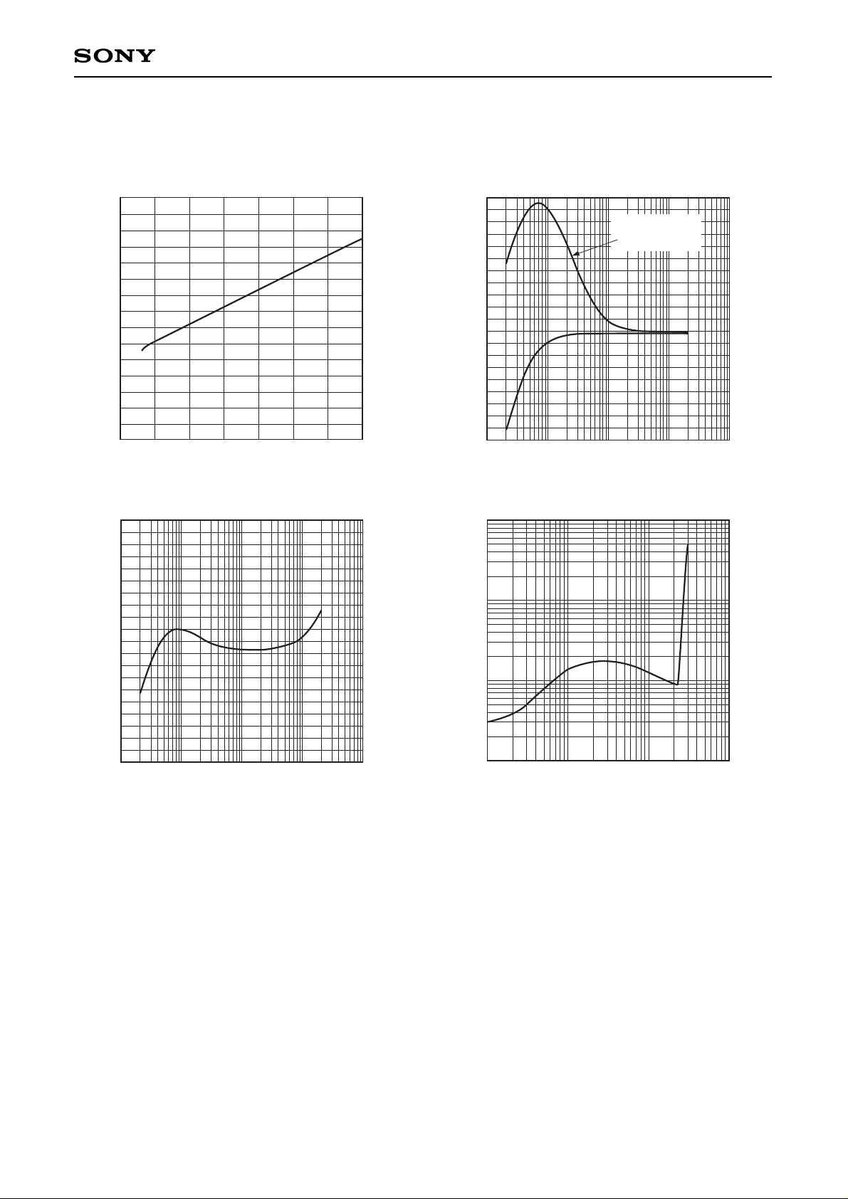
Example of Representative Characteristics
Circuit current (at no signal)
VCC [V]
ICC [mA]
3.0 3.5 4.0 4.51.5
2.5
3.0
3.2
2.9
3.1
2.7
2.6
2.8
3.6
3.7
3.4
3.3
3.5
3.8
3.9
4.0
2.0 2.5 5.0
Distortion factor vs. Input characteristics
Input [Vpk]
Distortion factor [%]
0.10.001
0.01
0.1
1
10
0.01 1
Crosstalk vs. Frequency
Frequency [Hz]
Crosstalk [dB]
1k 10k10
–60
–55
–53
–56
–54
–58
–59
–57
–49
–48
–51
–52
–50
–43
–42
–45
–44
–41
–46
–47
–40
100 100k
Frequency characteristic
Frequency [Hz]
Gain [dB]
1k 10k10
3.0
8.0
10.0
7.0
9.0
5.0
4.0
6.0
14.0
15.0
12.0
11.0
13.0
16.0
17.0
18.0
19.0
20.0
22.0
21.0
23.0
Bass Boost On
C = 0.1µF
100 100k
Page 12
– 12 –
CXA2566M
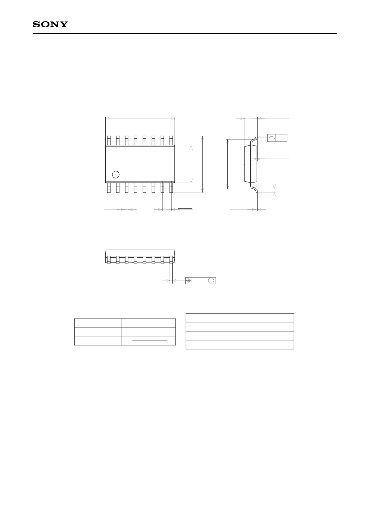
Package Outline Unit: mm
PACKAGE STRUCTURE
PACKAGE MATERIAL
LEAD TREATMENT
LEAD MATERIAL
PACKAGE MASS
SONY CODE
EIAJ CODE
JEDEC CODE
SOP-16P-L01
SOP016-P-0300
COPPER ALLOY
SOLDER PLATING
EPOXY RESIN
16PIN SOP (PLASTIC)
9.9 – 0.1
+ 0.4
16
9
1 8
1.27
0.45 ± 0.1
5.3 – 0.1
+ 0.3
7.9 ± 0.4
6.9
1.85 – 0.15
+ 0.4
0.5 ± 0.2
0.2 – 0.05
+ 0.1
0.1 – 0.05
+ 0.2
0.2g
0.15
M
0.24
 Loading...