

Page 1
10-bit 125MSPS D/A Converter
Description
The CXA3197R is a high-speed D/A converter
which can perform multiplexed input of two system
10-bit data.
This IC realizes a maximum conversion rate of
125MSPS. Multiplexed operation is possible by
inputing the 1/2 frequency-divided clock or by halving
the frequency of the clock internally with the clock
frequency divider circuit having the reset pin. The
data input is at TTL level, and the clock input and
reset input can select either TTL or PECL level
according to the application.
Features
• Maximum conversion rate:
During PECL operation: 125MSPS
During TTL operation: 100MSPS
• Resolution: 10 bits
• Low power consumption: 480mW (typ.)
• Data input level: TTL
• Clock, reset input level: TTL and PECL compatible
• 2:1 multiplexed input function
• 1/2 frequency-divided clock output possible by the
built-in clock frequency divider circuit
• Voltage output (50Ω load drive possible)
• Single power supply or ±dual power supply operation
• Reset signal polarity switching function
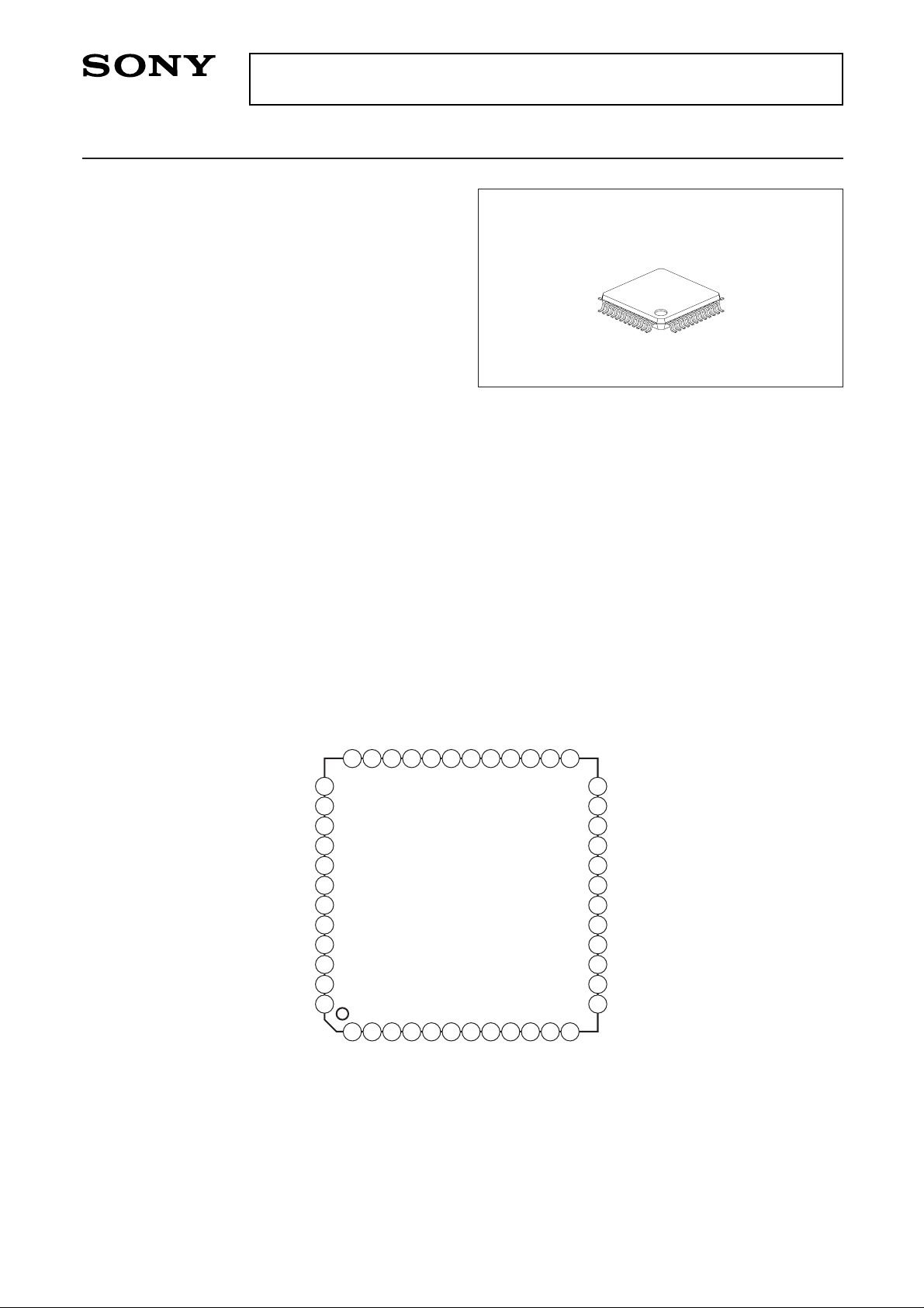
Pin Configuration
Structure
Bipolar silicon monolithic IC
Applications
• LCD
• DDS
• HDTV
• Communications (QPSK, QAM)
• Measuring devices
– 1 –
E97639-PS
Sony reserves the right to change products and specifications without prior notice. This information does not convey any license by
any implication or otherwise under any patents or other right. Application circuits shown, if any, are typical examples illustrating the
operation of the devices. Sony cannot assume responsibility for any problems arising out of the use of these circuits.
CXA3197R
48 pin LQFP (Plastic)
13
14
15
16
17
18
19
20
21
22
23
24
25
26
2728
29
30
36
35
34
31
32
33
40
39
38
37
41
42
43
44
45
46
47
48
2
3
4
5
6
7
8
9
10
11
12
1
DA5
DA4
DA3
DA2
DA1
(LSB) DA0
(MSB) DB9
DB8
DB7
DB6
DB5
DB4
AV
CC
2
VSET
VREF
AGND2
AOUTP
AV
CC
O
AOUTN
DV
CC
2
C3
C2
C1
DGND2
DB3
DB2
DB1
DB0 (LSB)
DIV2IN
DIV2OUT
CLK/T
CLKP/E
CLKN/E
RESET/T
RESETP/E
RESETN/E
DA6
DA7
DA8
(MSB) DA9
DGND1
N.C.
DV
CC1
PS
INV
R POLARITY
VOCLP
AGND2
LEAD TREATMENT: PALLADIUM PLATING
Page 2
– 2 –
CXA3197R
Absolute Maximum Ratings (Ta = 25°C)
• Supply voltage AVCCO, AVCC2, DVCC2 –0.5 to +6.0 V
AGND2, DGND2 –6.0 to +0.5 V
DVCC1 –0.5 to +6.0 V
AVCC2 – AGND2 –0.5 to +6.0 V
AVCCO – AGND2 –0.5 to +6.0 V
DVCC2 – DGND2 –0.5 to +6.0 V
• Input voltage
(Analog) VSET AGND2 – 0.5 to AVCC2 + 0.5 V
(Digital) TTL input pin DGND1 – 0.5 to DVCC1 + 0.5 V
PECL input pin DGND1 – 0.5 to DVCC1 + 0.5 V
PS DGND1 – 0.5 to DVCC1 + 0.5 V
(Others) VOCLP DGND1 – 0.5 to DVCC1 + 0.5 V
• Storage temperature Tstg – 65 to +150 °C
• Allowable power dissipation Pd 1.4 W
(when mounted on a two-layer glass fabric base epoxy board with dimensions of 76mm × 114mm, t = 1.6mm)
Recommended Operating Conditions
[Single power supply] [Dual power supply]
• Supply voltage Min. Typ. Max. Min. Typ. Max. Unit
AVCCO +4.75 +5.0 +5.25 –0.05 0.0 +0.05 V
AVCC2 +4.75 +5.0 +5.25 –0.05 0.0 +0.05 V
AGND2 –0.05 0.0 +0.05 –5.50 –5.0 –4.75 V
DVCC1 +4.75 +5.0 +5.25 +4.75 +5.0 +5.25 V
DGND1 –0.05 0.0 +0.05 –0.05 0.0 +0.05 V
DVCC2 +4.75 +5.0 +5.25 –0.05 0.0 +0.05 V
DGND2 –0.05 0.0 +0.05 –5.50 –5.0 –4.75 V
• Input voltage Min. Typ. Max. Unit
(Analog) VSET AGND2 + 0.65 AGND2 + 1.03 V
(Digital) TTL input pin VIH DGND1 + 2.0 V
VIL DGND1 + 0.8 V
PECL input pin VIH DVCC1 – 1.05 DVCC1 – 0.5 V
VIL DVCC1 – 3.2 DVCC1 – 1.4 V
VID
∗1
0.5 0.8 V
(Others) VOCLP DGND1 + 2.4 DVCC1 V
• CLK pulse width (for RECL CLK) tpw1 3.5 ns
tpw0 3.5 ns
• Maximum conversion rate During PECL operation Fc 125 MSPS
During TTL operation Fc 100 MSPS
• Load resistance RL 50 50 ≥ 10k Ω
• Analog output full-scale voltage
RL ≥ 10kΩ VFS 1.5 2.0 2.1 V
RL = 50Ω VFS 0.75 1.0 1.05 V
• Operating temperature Ta –20 +75 °C
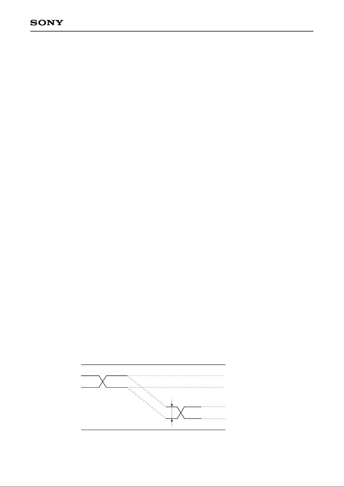
∗1
VID: Input Voltage Differential
PECL input signal switching level
VIH
VIL (Min.)
V
IH (Max.)
V
IL
DVCC1
VID
DGND1
Page 3

– 3 –
CXA3197R
Pin Description
[Symbol] [Pin No.] [Description]
DA0 to DA9 1 to 6, 45 to 48 Side A data input. TTL TTL
DB0 to DB9 7 to 16 Side B data input. TTL TTL
DIV2IN 17 1/2 frequency-divided clock input. TTL TTL
DIV2OUT 18 1/2 frequency-divided clock output. TTL TTL
CLK/T 19 TTL clock input. TTL TTL
CLKP/E 20 PECL clock input. PECL PECL
CLKN/E 21 PECL clock input. PECL PECL
RESET/T 22 TTL reset input. TTL TTL
RESETP/E 23 PECL reset input. PECL PECL
RESETN/E 24 PECL reset input. PECL PECL
DGND2 25 Digital ground. 0V –5V
C1 26 Function setting. TTL TTL
C2 27 Function setting. TTL TTL
C3 28 Function setting. TTL TTL
DVCC2 29 Digital power supply. 5V 0V
AVCCO 30 Analog output power supply. 5V (typ.) 0V (typ.)
AOUTN 31 Negative analog output. AVCCO – VFS AVCCO – VFS
AOUTP 32 Positive analog output. AVCCO – VFS AVCCO – VFS
AGND2 33 Analog ground. 0V –5V
VREF 34 Analog reference voltage. AGND2 + 1.25V AGND2 + 1.25V
VSET 35 Full-scale adjustment.
AVCC2 36 Analog power supply. 5V 0V
AGND2 37 Analog ground. 0V –5V
VOCLP 38 TTL High level clamp. Clamp voltage Clamp voltage
R POLARITY 39 Reset signal polarity switching. TTL TTL
INV 40 Analog output inversion. TTL TTL
PS 41 Power saving. TTL TTL
DVCC1 42 Digital power supply. 5V 5V
N.C. 43 Not connected. — —
DGND1 44 Digital ground. 0V 0V
[
Typical voltage level for
]
a single power supply
[
Typical voltage level
]
for dual power supply
AGND2 + 0.65V
to
AGND2 + 1.03V
AGND2 + 0.65V
to
AGND2 + 1.03V
Page 4
– 4 –
CXA3197R
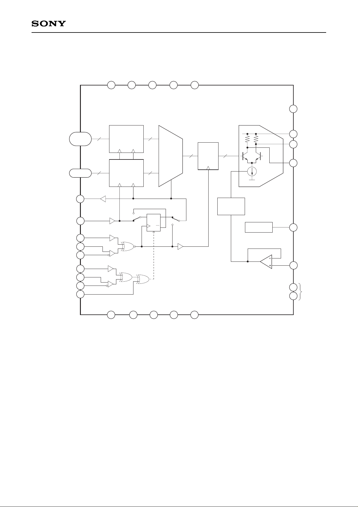
Block Diagram
VSET
VREF
29
DVCC2
28
C3
27
C2
26
C1
25
DGND2
DIV2IN
CLK/T
CLKP/E
CLKN/E
RESET/T
RESETP/E
RESETN/E
44
DGND1
42
DV
CC1
41
PS
40
INV
R POLARITY
38
VOCLP
AOUTP
AV
CCO
AOUTN
36
AVCC2
Input Latch
B
10bit 10bit
Input Latch
A
10bit 10bit
MUX
10bit
Latch
10bit
BGR
35
34
Current
Cont.
1 to 6
45 to 48
7 to 16
DA0 to DA9
DB0 to DB9
AGND2
RO = 50Ω
30
31
32
D Q
Q
22
23
24
39
AGND2
33
37
17
19
20
21
18
DIV2OUT
Page 5

– 5 –
CXA3197R
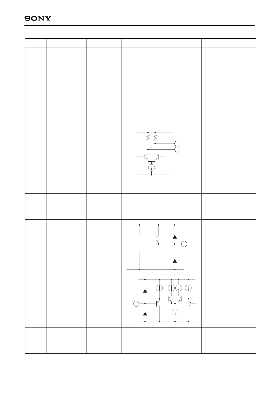
Pin Description and I/O Pin Equivalent Circuit
Side A data input.
Side B data input.
1/2 frequency-divided
clock input.
Use this pin in MUX.1A
or MUX.2 mode.
Leave open for other
modes.
1/2 frequency-divided
clock output.
The 1/2 frequencydivided clock signal
(DIV2OUT) is output in
MUX.1A mode.
Set to high impedance
for other modes.
DA0 to DA9
DB0 to DB9
DIV2IN
DIV2OUT
TTL
TTL
TTL
TTL
1 to 6
45 to 48
7 to 16
17
18
I
I
I
O
DVCC1
DGND1
6
1
45
48
7
16
to
to
to
1.5V
DVCC1
DGND1
17
1.5V
DVCC1
DGND1
18
100K
Clock input.
Use this pin when the
clock is input at TTL
level.
At this time, leave Pins
20 and 21 open.
CLK/T TTL19 I
DVCC1
DGND1
19
1.5V
Pin No. Symbol
Typical voltage level
Equivalent circuit DescriptionI/O
Page 6

– 6 –
CXA3197R
Clock input.
Use this pin when the
clock is input at PECL
level.
At this time, leave
Pin 19 open.
CLKP/E and CLKN/E
are complementary and
should be used together.
CLKP/E complementary
input.
Reset signal input.
When multiple
CXA3197R are
operated at the same
time in MUX.1A or
MUX.1B mode, the start
timing of the internal 1/2
frequency divider
circuits should be
matched.
At this time, the reset
signal is used; when the
reset signal is at TTL
level, Pin 22 is used and
Pins 23 and 24 are left
open. When the reset
signal is at PECL level,
Pins 23 and 24 are used
and Pin 22 is left open.
The reset signal polarity
can be set by Pin 39
(R POLARITY).
Leave the reset pin
open when other modes
are used.
RESETP/E and
RESETN/E are
complementary and
should be used together.
CLKP/E PECL20
I
CLKN/E PECL
21
I
RESET/T
TTL
22
I
RESETP/E PECL23 I
RESETN/E
PECL
24
I
DGND2
Single power
supply: GND
Dual power
supply: –5V
25
DVCC1
DGND1
20
21
Function setting.
Function setting.
Function setting.
C1 TTL26 I
C2 TTL27 I
C3
TTL
28
I
26
28
DVCC1
DGND1
27
1.5V
DVCC1
DGND1
22
1.5V
DVCC1
DGND1
23
24
Digital power supply.
Pin No. Symbol
Typical voltage level
Equivalent circuit DescriptionI/O
Page 7
– 7 –
CXA3197R
DVCC2
29
32
AVCCO
AGND2
31
RORO
Digital power supply.
Analog output power
supply.
The AVCCO pin voltage
can be varied within the
range that satisfies the
analog output
compliance voltage.
Positive analog output.
Analog ground.
Negative analog output.
The inverse of the
positive analog output
pin is output.
When the positive
output is terminated with
50Ω, the inverse output
pin should also be
terminated with 50Ω
even if the inverse
output is not used.
AVCCO
Single power
supply: +5V
Dual power
supply: GND
30
AOUTN
AVCCO – VFS
31
O
AOUTP
AVCCO – VFS
32
O
Single power
supply: +5V
Dual power
supply: GND
Reference voltage
output.
AVCC2
AGND2
34
BGR
AGND2
Single power
supply: GND
Dual power
supply: –5V
33
VREF
AGND + 1.25V
(Typ.)
34
O
Analog output full-scale
adjustment.
VSET
AGND2 + 0.65V
to
AGND2 + 1.03V
35 I
AVCC2
35
AGND2
Pin No. Symbol
Typical voltage level
Equivalent circuit DescriptionI/O
AVCC2
36
Analog power supply.
Single power
supply: +5V
Dual power
supply: GND
Page 8

– 8 –
CXA3197R
TTL output High level
clamp.
A TTL level signal is
output from the
DIV2OUT pin in
MUX.1A mode. The
TTL High level voltage
can be clamped to the
value approximately
equivalent to the voltage
applied to this pin.
Leave the VOCLP pin
open for other modes.
VOCLP
Clamp voltage
38
I
DVCC1
DGND1
38
Reset signal polarity
switching.
At High level, the reset
polarity is active Low; at
Low level, active High.
R POLARITY
TTL
39
I
DVCC1
DGND1
39
1.5V
Analog output polarity
inversion.
The analog output is
inverted at Low level.
INV TTL
40
I
DVCC1
DGND1
40
1.5V
Power saving.
Power saving mode is
activated at Low level.
Normally pull up the PS
pin to High level as this
pin is open Low.
PS TTL41 I
DVCC1
42
DVCC1
DGND1
41
Digital power supply.
5V
N.C.
43
Not connected.
DGND1
44
Digital ground.
0V
Pin No. Symbol
Typical voltage level
Equivalent circuit DescriptionI/O
Analog power supply.
AGND2
Single power
supply: GND
Dual power
supply: –5V
37
Page 9
– 9 –
CXA3197R
Resolution
Differential linearity error
Integral linearity error
Digital input (PECL)
Digital input voltage
Digital input current
Digital input capacitance
Digital input (TTL)
Digital input voltage
Threshold voltage
Digital input current
Digital input capacitance
Digital output (TTL)
Digital output voltage
Leak current at high impedance
Digital output rise time
Digital output fall time
PS pin input (PS)
PS pin input voltage
PS pin input current
Clamp pin (VOCLP)
VOCLP pin input current
Analog output characteristics
Output full-scale voltage
: RL ≥ 10kΩ
: RL = 50Ω
Output zero offset voltage
: RL ≥ 10kΩ
: RL = 50Ω
Analog output resistance
Analog output capacitance
Absolute amplitude error
Absolute amplitude error
temperature characteristics
Analog output rise time
Analog output fall time
Settling time
Glitch energy
Compliance voltage
n
DLE
ILE
VIH
VIL
IIH
IIL
VIH
VIL
VTH
IIH
IIL
VOH
VOL
Tr
Tf
VIH
VIL
IIH
IIL
IVOCLP
IVOCLP
VFS
VFS
VOF
VOF
RO
CO
EG
TCG
Tr
Tf
tSET
GE
VOC
VFS = 1000mV
∗2
VIH = DVCC1 – 0.8V
VIL = DVCC1 – 1.6V
VIH = 3.5V
VIL = 0.2V
IOH = –2.0mA
IOL = 1.0mA
When VO = 5V
When VO = 0V
0.8 to 2.4V (CL = 10pF)
0.8 to 2.4V (CL = 10pF)
VIH = 3.5V
VIL = 0.2V
VOCLP = DVCC1
VOCLP = 2.4V
VSET = AGND2 + 937.5mV
VSET = AGND2 + 937.5mV
VFS = 1000mV at 25°C
When RL = 50Ω,
VFS = 1V,10 – 90%
Mesured to DVCC2
∗3
10
DVCC1 – 1.05
DVCC1 – 3.2
0
–30
2
–1
–2
2.4
10
–1
1
0.6
2
1
–1
0
–60
1.5
0.75
0
0
–4.0
0.85
0.75
–2.1
10
1.5
2
1
50
10
10
–0.85/+0.5
–1.2/+0.5
±1.2
DVCC1 – 0.5
DVCC1 – 1.4
20
0
5
0.8
1
0
5
0.5
100
1
1.5
1.2
0.8
100
0
5
–10
2.1
1.05
20
10
4.0
60
1.05
0.85
3.5
5
1.5
bit
LSB
LSB
LSB
V
V
µA
µA
pF
V
V
V
µA
µA
pF
V
V
µA
µA
ns
ns
V
V
µA
µA
µA
µA
V
V
mV
mV
Ω
pF
% of F.S.
ppm/°C
ns
ns
ns
pVsec
V
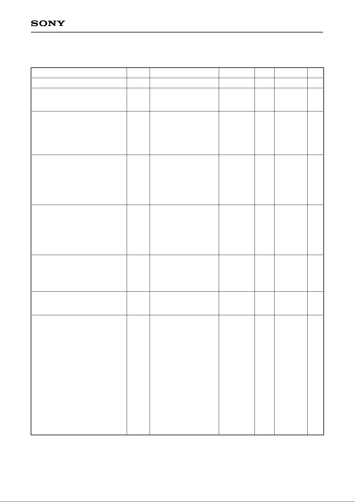
Electrical Characteristics
(DVCC1, DVCC2, AVCC2, AVCCO = +5V, DGND1, DGND2 = 0V, Ta = 25°C)
Item
Symbol
Conditions
Min.
Typ.
Max. Unit
}
}
Page 10

– 10 –
CXA3197R
Reference/control amplifier
characteristics
VREF pin output voltage
VREF pin output voltage
in PS mode
VREF voltage drift
coefficient
VSET pin input current
Multiplying bandwidth
Current consumption
Current consumption in PS
mode
∗4
VREF
VREF
ISET
ICC
DICC1
DICC2
AICC2
AICCO
ICC
DICC1
DICC2
AICC2
AICCO
IREFOUT = 1mA
100mVp-p, SIN,
at –3dB
Total current
consumption
DIcc1 current
consumption
DIcc2 current
consumption
AIcc2 current
consumption
AIccO current
consumption
Total current
consumption in PS
mode
DIcc1 current
consumption in PS
mode
DIcc2 current
consumption in PS
mode
AIcc2 current
consumption in
PS mode
AIccO current
consumption in
PS mode
AGND2 + 1.18
AGND2 + 1.18
–5
50
63
7
13
6
37
AGND2 + 1.25
AGND2 + 1.25
96
15.5
19
8.5
53
0.432
0.38
0.001
0.05
0.001
AGND2 + 1.32
AGND2 + 1.32
250
0
129
24
25
11
69
4
1.5
0.2
0.3
2
V
V
ppm/°C
µA
MHz
mA
mA
mA
mA
mA
mA
mA
mA
mA
mA
}
Item
Symbol
Conditions
Min.
Typ.
Max. Unit
∗2
64-step D.L.E. This indicates the D.L.E. when the INV pin is High and the data input code changes between:
at the AOUTP side output or between:
at the AOUTN side output.
(MSB) (LSB) (MSB) (LSB)
0 0 0 0 1 1 1 1 1 1 0 0 0 1 0 0 0 0 0 0
←→
(MSB) (LSB) (MSB) (LSB)
1 1 1 1 0 0 0 0 0 0 1 1 1 0 1 1 1 1 1 1
←→
∗3
When using the analog output within the compliance voltage range, set AVCCO so that it satisfies the
following equations.
VOC (min) = (AVCCO – VFS) – DVCC2 ≥ –2.1V
VOC (max) = (AVCCO – VOF) – DVCC2 ≤ 1.5V
Page 11
– 11 –
CXA3197R
∗4
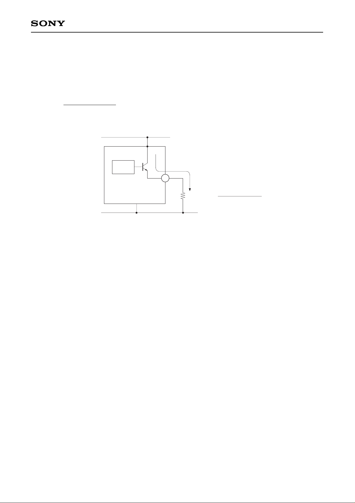
The current consumption in power saving mode does not include the VREF pin output current. When
grounding the VREF pin to the AGND2 level using external resistance, a voltage of 1.18 to 1.32V is
generated at the VREF pin even in power saving mode. Therefore, the current indicated by the following
equation flows from the AVCC2 pin to the VREF pin. This value must be added to obtain the actual current
consumption in power saving mode.
VREF pin voltage
External resistance
= IREFOUT
VREF pin voltage
External resistance
BGR
AVCC2
AGND2
In power saving mode:
IREFOUT =
34
VREF
Page 12

– 12 –
CXA3197R
Item
Maximum conversion rate
Clock High pulse width
Clock Low pulse width
Reset signal setup time
Reset signal hold time
DIV2OUT output delay
DIV2OUT to DIV2IN maximum delay time
Data input setup time
Data input hold time
Analog output pipeline delay
Analog output delay
Maximum conversion rate
Clock High pulse width
Clock Low pulse width
Reset signal setup time
Reset signal hold time
Data input setup time
Data input hold time
Analog output pipeline delay
Analog output delay
Symbol
FC
Tpw1
Tpw0
ts-rst
th-rst
td-DIV
2T-tm
ts
th
t
PD (A)
tPD (B)
tdo FCTpw1
Tpw0
ts-rst
th-rst
ts
th
tPD (A)
tPD (B)
tdo
Conditions
C
L = 10pF
Min. Typ. Max.
125
3.5
3.5
0
1.0
5.5
1.0
5.0
5.0
125
3.5
3.5
0
1.0
1.0
4.0
5.0
6.5
4
5
5.5
2
3
5.5
8
2T – 7
6.0
6.0
Switching characteristics
MUX.1A mode
Min. Typ. Max.
100
4.5
3.0
1.0
3.0
8.0
1.0
5.0
6.5
100
4.5
3.0
1.0
3.0
1.0
6.0
6.5
9.5
4
5
7.5
2
3
7.5
12.0
2T – 7
8.5
8.5
Min. Typ. Max. Unit
125
3.5
3.5
4.0
0
5.5
1.0
5.0
5.0
125
3.5
3.5
4.0
0
1.0
4.0
5.0
6.5
4
5
5.5
2
3
5.5
8
2T – 7
6.0
6.0
MSPS
ns
ns
ns
ns
ns
ns
ns
ns
CLK
ns
MSPS
ns
ns
ns
ns
ns
ns
CLK
ns
CLK signal level
Reset signal level
PECL
PECL
TTL
TTL
PECL
TTL
MUX.1B mode
Page 13

– 13 –
CXA3197R
Item
Maximum conversion rate
Clock High pulse width
Clock Low pulse width
DIV2IN setup time
DIV2IN hold time
Data input setup time
Data input hold time
Analog output pipeline delay
Analog output delay
Maximum conversion rate
Clock High pulse width
Clock Low pulse width
C2 signal setup time
C2 signal hold time
Data input setup time
Data input hold time
Analog output pipeline delay
Analog output delay
Symbol
FC
Tpw1
Tpw0
ts-DIV
th-DIV
ts
th
t
PD (A)
tPD (B)
tdo
FC
Tpw1
Tpw0
ts-C2
th-C2
ts
th
tPD (A)
tPD (B)
tdo
Conditions Min. Typ. Max.
125
3.5
3.5
4.5
0
1.0
5.0
5.0
125
3.5
3.5
1.0
2.5
1.0
2.0
5.0
2
3
5.5
1
1
5.5
6.0
6.0
Switching characteristics
MUX.2 mode
SELE.A, SELE.B modes
Min. Typ. Max.
100
4.5
3.0
2.0
3.5
1.0
5.0
6.5
100
4.5
3.0
1.0
3.5
1.5
3.5
6.5
2
3
7.5
1
1
7.5
8.5
8.5
Unit
MSPS
ns
ns
ns
ns
ns
ns
CLK
ns
MSPS
ns
ns
ns
ns
ns
ns
CLK
ns
CLK signal level
Reset signal level
PECL
—
∗
4
TTL
—
∗4
∗4
The reset signal is not input in MUX.2, SELE.A or SELE.B mode.
Page 14
– 14 –
CXA3197R
50Ω
10
DA0
to
DA9
10
DB0
to
DB9
CLK/T
10-bit Data input
+5V
DVCC1 DGND1
DVCC2
AVCC2
AVCCO
AOUTP
AOUTN
VSET
DGND2
AGND2
937.5mV
–5V
–5V
+5V
DVM
(Digital
Voltmeter)
50Ω
C1 C2 C3
1MHz TTL CLK
CXA3197R
PC
+5V
I1 I2 I3 I4
DVCC1 DVCC2 AVCC2 AVCCO
10
DA0
to
DA9
10
DB0
to
DB9
DIV2IN
High for all side A data
1MHz TTL CLK
937.5mV
AOUTP
AOUTN
VSET
DGND1
DGND2
AGND2
C1 C2 C3
Low for all side B data
+5
CLK/T
DIV2OUT
PS
CXA3197R
I
CC = I1 + I2 + I3 + I4
DICC1 = I1
DICC2 = I2
AICC2 = I3
AICCO = I4
50Ω
10
DA0
to
DA9
10
DB0
to
DB9
CLK/T
+5V
DV
CC1 DGND1
DVCC2
AVCC2
AVCCO
AOUTP
AOUTN
VSET
DGND2
AGND2
937.5mV
–5V
–5V
+5
C1 C2 C3
1MHz TTL CLK
CXA3197R
50Ω
+5
INV
High for all side A data
Low for all side B data
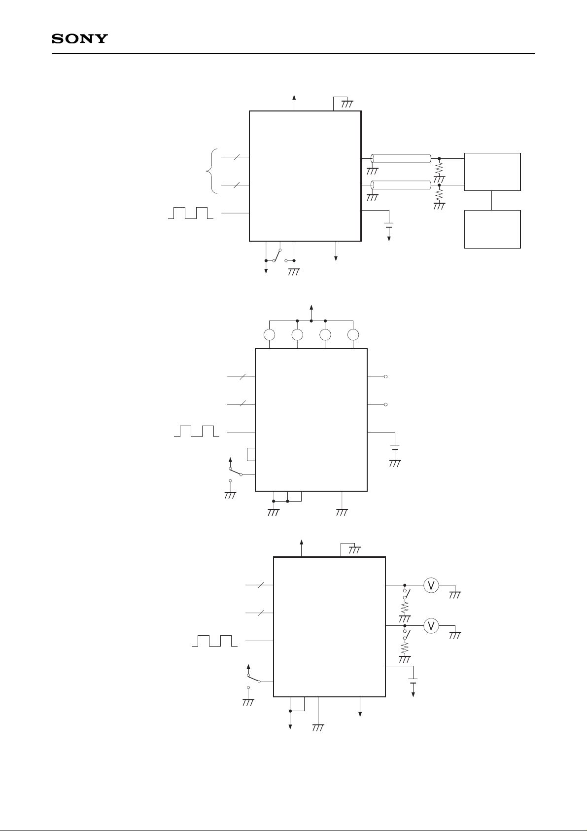
Electrical Characteristics Measurement Circuits
Differential Linearity Error
Integral Linearity Error
Current Consumption
Analog Output Characteristics
Output Full-Scale Absolute Amplitude Error
Output Zero Offset Voltage
Page 15

– 15 –
CXA3197R
10
DA0
to
DA9
10
DB0
to
DB9
100MHz PECL CLK
AOUTP
AOUTN
VREF
DGND2
AGND2
C1 C2 C3
CLKP/E
+5V
+5V
DV
CC1 DGND1
DVCC2
AVCC2
AVCCO
–5V
VSET
CLKN/E
CXA3197R
–5V
Oscilloscope
50Ω 50Ω
D. P. G.
(Digital
Pattern
Generator)
10
DA0
to
DA9
10
DB0
to
DB9
20MHz PECL CLK
AOUTP
AOUTN
VREF
DGND2
AGND2
C1 C2 C3
CLKP/E
+5V
+5V
DV
CC1 DGND1
DVCC2
AVCC2
AVCCO
–5V
VSET
CLKN/E
CXA3197R
–5V
50Ω
50Ω
50Ω
0.1µF
High for all side A data
High for all side B data
+5V
PS
Oscilloscope
VFS
AOUTP
output
VSET pin
output
AV
CCO
(= 0V)
AGND2
+ 937.5mV
100mVp-p
1mA
Analog Output Rise Time
Analog Output Fall Time
Settling Time
Glitch Energy
Reference/Control Amplifier Characteristics
VREF Pin Output Voltage
VREF Pin Output Voltage in Power Saving Mode
Multiplying Bandwidth
Page 16
– 16 –
CXA3197R
Data input code Analog output level
AOUTP
AVCCO – VOF
:
AVCCO – VFS
AVCCO – VFS
:
AVCCO – VOF
AOUTN
INV = 1
(MSB) (LSB)
D9 D0
1 1 1 1 1 1 1 1 1 1
:
0 0 0 0 0 0 0 0 0 0
(MSB) (LSB)
D9 D0
0 0 0 0 0 0 0 0 0 0
:
1 1 1 1 1 1 1 1 1 1
INV = 0
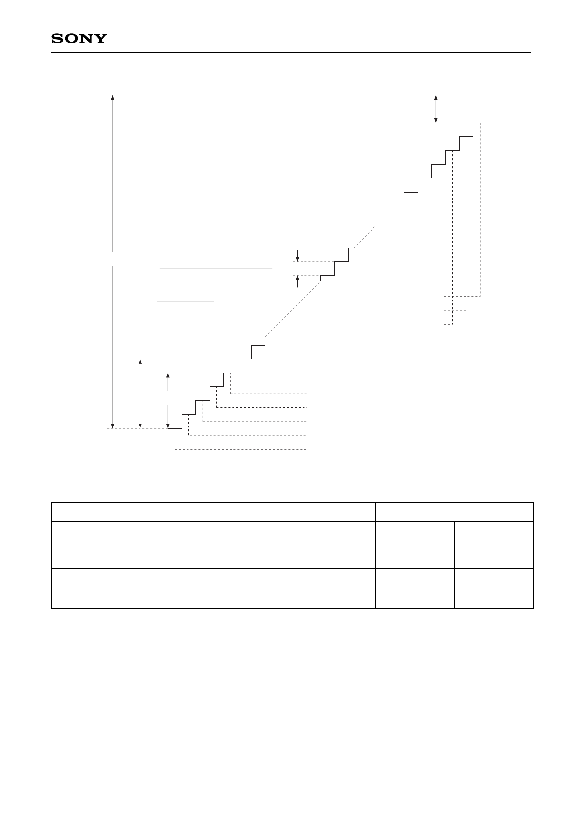
Table 1. I/O Correspondence Table
1111111111
0111111111
1011111111
0010000000
1100000000
0100000000
1000000000
0000000000
D0D9 Data input code
(LSB)
·
·
·
·
·
·
·
·
·
·
·
V (n)
V (n + 1)
AVCCO – VFS
AVCCO
AV
CCO – VOF
AOUTP output
(INV = 1)
(AV
CCO – VOF) – (AVCCO – VFS)
1023
= 1LSB
V (n + 1) – V (n)
1LSB
D.L.E. = –1
V (n) – n × 1LSB
1LSB
I.L.E. =
(MSB)
Page 17

– 17 –
CXA3197R
Description of Operation
The CXA3197R has four types of operation modes to support various applications. The operation mode is set
by switching the function setting pins (C1, C2 and C3).
Operation Mode Table
The CXA3197R can input data divided into two systems: A (DA0 to DA9) and B (DB0 to DB9), internally
multiplex the data, and output it as an analog signal, making it possible to halve the data rate. This lets the
CXA3197R support the TTL data input level in contrast to the ECL data input level for conventional high-speed
D/A converters. The clock signal and reset signal input levels can be selected from either TTL or PECL
according to the application. (However, setting both signals to either TTL or PECL input level is
recommended.)
Mode
MUX.1A
MUX.1B
MUX.2
SELE.A
SELE.B
0
0
0
1
1
0
0
1
0
1
0
1
0
0
0
125
62.5
125
125
C1 C2 C3
CLK IN
(MSPS)
Data IN
(Mbps)
AOUT
(Mbps)
DIV2OUT pin Description of operation
MUX operation by the internal
CLK/2
MUX operation by the internal
CLK/2
MUX operation by DIV2IN
D/A conversion of side A data
input
D/A conversion of side B data
input
Outputs CLK/2 at TTL level
High impedance
High impedance
High impedance
High impedance
1. MUX.1A mode
Set C1, C2 and C3 all Low for this mode.
In MUX.1A mode, the frequency of the clock input from the clock input pin is halved internally, and the 1/2
frequency-divided signal is output at TTL level from the DIV2OUT pin. Data synchronized with the DIV2OUT
signal (the signal output from the DIV2OUT pin) can be obtained by operating the CXA3197R front-end system
with the DIV2OUT signal. The timing at which the data output delay of the CXA3197R front-end system
matches with the hold time during CXA3197R data input can be easily set by inputting this synchronized data
to the data input pins and the DIV2OUT signal to the DIV2IN pin. The data can be divided and input to two
systems: A (DA0 to DA9) and B (DB0 to DB9), internally multiplexed, and extracted as analog output.
10bit
10bit
Clock input
td – DIV
10bit Data. A
10bit Data. B
CXA3197R
front-end
system
Front-end system data output delay
CXA3197R data input hold time
=
(DIV2OUT signal)
Clock input pin
DA0 to DA9
CXA3197R (MUX.1A mode)
1/2
Data input pins
DB0 to DB9
DIV2OUT pin
DIV2IN pin
Page 18
– 18 –
CXA3197R
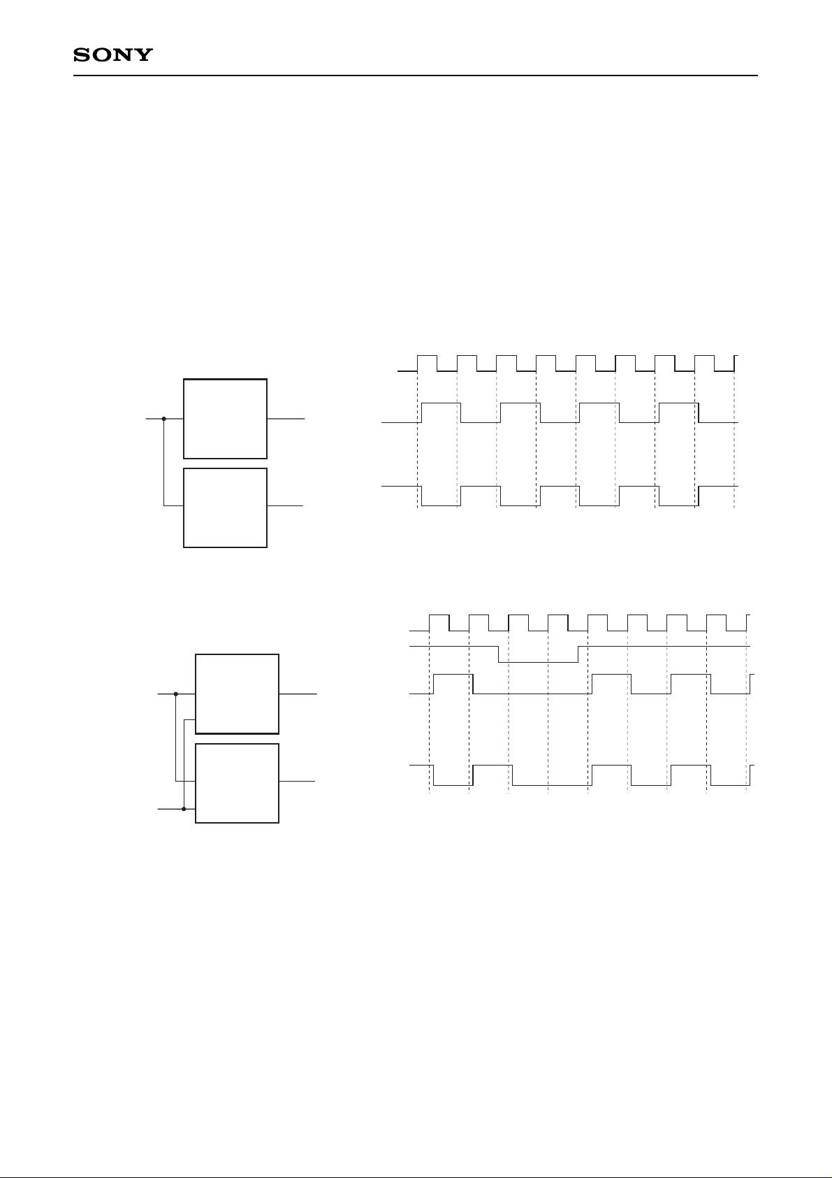
When using the multiple CXA3197R in MUX.1A mode, the start timing of the 1/2 frequency-divided clocks
becomes out of phase, producing operation such as that shown in the example below. As a countermeasure,
the MUX.1A mode has a function that matches the start timing of the 1/2 frequency-divided clocks with the
reset signal. When using a PECL level reset signal, input the reset signal to Pins 23 and 24 (RESETP/E,
RESETN/E) and leave Pin 22 (RESET/T) open. When using a TTL level reset signal, input the reset signal to
Pin 22 (RESET/T) and leave Pins 23 and 24 (RESETP/E, RESETN/E) open. The reset polarity can be
switched by the R POLARITY pin (Pin 39). When the R POLARITY pin is High or open, reset is active Low;
when Low, reset is active High. See the timing chart for the detailed timing.
CLK CLK DIV2OUT
CLK DIV2OUT
CLK
DIV2OUT
DIV2OUT
CXA3197R
CXA3197R
Example when not using the reset signal
Reset signal
(when active Low)
CLK DIV2OUT
CLK DIV2OUT
CLK
Reset signal
CLK
DIV2OUT
DIV2OUT
CXA3197R
CXA3197R
RESET
RESET
Example when using the reset signal
Page 19
– 19 –
CXA3197R
2. MUX.1B mode
Set C1 and C2 Low and C3 High for this mode.
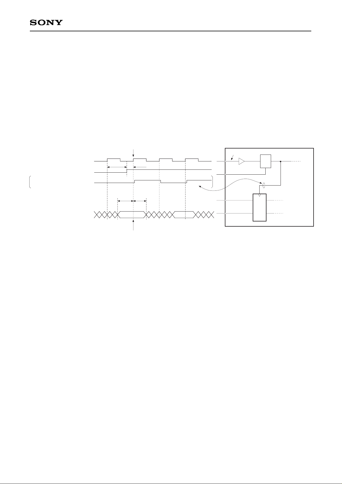
In MUX.1B mode, the frequency of the clock input from the clock input pin is halved internally, and the data is
loaded by this 1/2 frequency-divided signal. The 1/2 frequency-divided signal cannot be observed at this time,
so the data is actually loaded by observing the clock and reset signals to estimate the rising edge of the
internally 1/2 frequency-divided signal. The data can be divided and input to two systems: A (DA0 to DA9) and
B (DB0 to DB9). The data is internally multiplexed, then the system A data is output as an analog signal with a
2-clock pipeline delay, and the system B data as an analog signal with a 3-clock pipeline delay after loading by
the clock.
Clock
th-rst
After the reset is released, the internal 1/2 frequency-divided signal commences at the first clock edge,
so be sure to input the data in a manner that satisfies the setup time (ts) and hold time (th) with respect
to this clock edge.
Clock input pin
DA0 to DA9
CXA3197R (MUX.1B mode)
1/2
Reset input pin
DB0 to DB9
ts-rst
ts th
Reset signal
(when active Low)
Internally 1/2 frequency-divided signal
(This signal cannot be observed.)
Data input signal
Page 20
– 20 –
CXA3197R
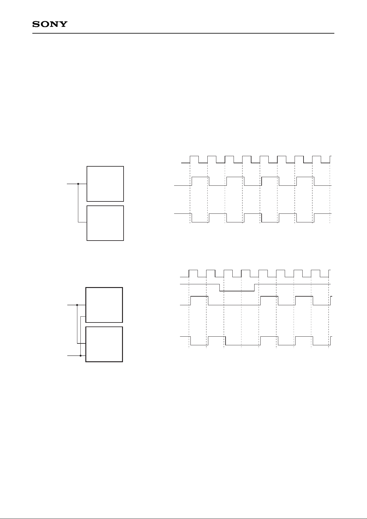
Like MUX.1A mode, when using the multiple CXA3197R in MUX.1B mode, the start timing of the 1/2
frequency-divided clocks becomes out of phase, producing operation such as that shown in the example
below. As a countermeasure, the MUX.1B mode also has a function that matches the start timing of the 1/2
frequency-divided clocks with the reset signal. When using a PECL level reset signal, input the reset signal to
Pins 23 and 24 (RESETP/E, RESETN/E) and leave Pin 22 (RESET/T) open. When using a TTL level reset
signal, input the reset signal to Pin 22 (RESET/T) and leave Pins 23 and 24 (RESETP/E, RESETN/E) open.
The reset polarity can be switched by the R POLARITY pin (Pin 39). When the R POLARITY pin is High or
open, reset is active Low; when Low, reset is active High. See the timing chart for the detailed timing.
CLK
Internally 1/2
frequency-divided
signal
CLK
CLK
CLK
CXA3197R
CXA3197R
Internally 1/2
frequency-divided
signal
Example when not using the reset signal
CLK
CLK
CLK
RESET signal
CLK
Reset signal
(when active Low)
Internally 1/2
frequency-divided
signal
Internally 1/2
frequency-divided
signal
CXA3197R
CXA3197R
RESET
RESET
Example when using the reset signal
Page 21
– 21 –
CXA3197R
3. MUX.2 mode
Set C1 and C3 Low and C2 High for this mode.
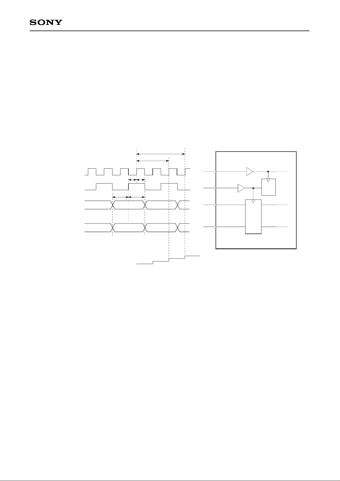
In MUX.2 mode, the clock is input to the clock input pin, and the signal with a cycle half that of the clock
(hereafter, DIV2IN signal) is input to the DIV2IN pin at TTL level. The DIV2IN signal is internally latched by the
clock, so consideration must be given to the setup time (ts_DIV) and hold time (th_DIV) with respect to the
clock. In addition, the data is loaded by the DIV2IN signal, so consideration must also be given to the setup
time (ts) and hold time (th) with respect to the DIV2IN signal. The data can be divided and input to two
systems: A (DA0 to DA9) and B (DB0 to DB9). The data is internally multiplexed, then the system A data is
output as an analog signal with a 2-clock pipeline delay, and the system B data as an analog signal with a 3clock pipeline delay from the clock that loads the DIV2IN signal. See the timing chart for the detailed timing.
thts
ts_DIV th_DIV
DA0 to DA9
CXA3197R (MUX.2 mode)
DB0 to DB9
Clock input pin
DIV2IN input pin
A0
B0
A1
A0
A1 A2
B0
B1 B2
Clock
DIV2IN signal
System A data
System B data
Analog output signal
B1
tPD (A)
t
PD (B)
0 1 2 3
Page 22

– 22 –
CXA3197R
4. SELE.A mode and SELE.B mode
Set C1 High and C2 and C3 Low for SELE.A mode.
In SELE.A mode, the clock is input to the clock input pin, and the data is input to the system A (DA0 to DA9)
data input pins.
Set C1 and C2 High and C3 Low for SELE.B mode.
In SELE.B mode, the clock is input to the clock input pin, and the data is input to the system B (DB0 to DB9)
data input pins.
In either mode, consideration must be given to the setup time (ts) and hold time (th) with respect to the clock.
Also, the data is output as an analog signal with a 1-clock pipeline delay after loading by the clock.
Switching between SELE.A mode and SELE.B mode is done by switching the C2 pin between High and Low
levels. Also, the mode can be switched at high speed in sync with the clock by inputting the switching signal
(C2 signal) to the C2 pin. The C2 signal is internally latched by the clock, so consideration must be given to the
setup time (ts_C2) and hold time (th_C2) with respect to the clock. See the timing chart for the detailed timing.
thts
ts_C2
DA0 to DA9
CXA3197R
(SELE.A mode/SELE.B mode)
DB0 to DB9
Clock input pin
C2 input pin
A0
A1
A2
A2 A6
Clock
C2 signal
System A data
System B data
Analog output signal
A1A0
B3
B4
B5
A6
B5 B7B4B3
Select
th_C2
A8
tPD (A) tPD (B)
0 1 0 1
Page 23
– 23 –
CXA3197R
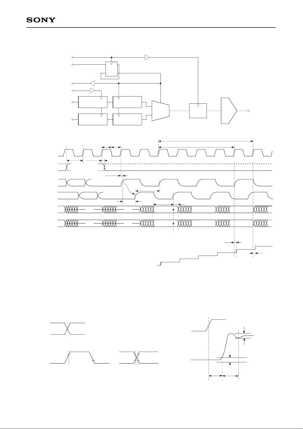
Block Diagram & Timing Chart (MUX.1A Mode)
ts
Latch
Latch
Input Latch B
LatchInput Latch A
D
Q
Q
DACMUX
R
CLK/2
(Internal)
Analog out
Input Data A
Input Data B
DIV2IN
DIV2OUT
RESET
CLK
th-rst
td-DIV
0 1 2
3
CLK
RESET
DIV2OUT
Input Data A
Input Data B
DIV2IN
N$
N$
N$
N$
N
N + 1
tdo
N$ N$ N + 3 N + 5N +1
N$ N$ N + 2 N + 4N
4
(Active High)
(Active Low)
Tpw1 Tpw0
ts-rst
tPD (A)
tm
th
tdo
tPD (B)
5
2T-tm
In MUX.1A mode, Data A and Data B are internally multiplexed and then the resulting signal can be analog
output. The frequency of the clock is halved by the built-in clock frequency divider circuit and the CLK/2 can be
output at TTL level (DIV2OUT). CLK/2 can be reset by the reset signal.
(Timing judgment points)
PECL
TTL
2.0V
0.8V
2.0V
0.8V
CLK
Analog output
tdo
t
SET
±1/2LSB
±1/2LSB
Page 24
– 24 –
CXA3197R
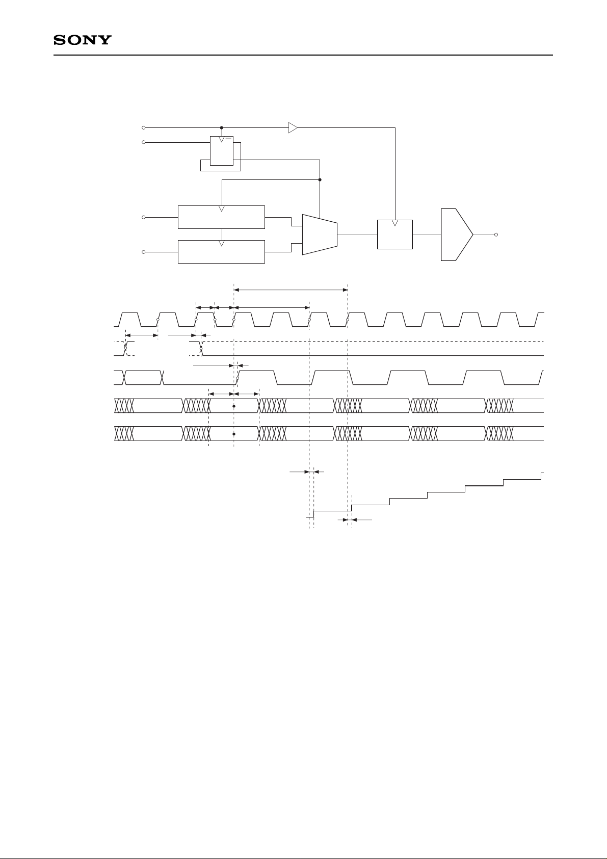
Block Diagram & Timing Chart (MUX.1B Mode)
Latch
Input Latch B
Input Latch A
D
Q
Q
DACMUX
R
CLK/2
(Internal)
Analog out
Input Data A
Input Data B
RESET
CLK
th-rst
D-FF out
CLK
RESET
(Active High)
CLK/2
(Internal)
Input Data A
Input Data B
N
N + 5
tdo
N – 1 N + 1 N + 5 N + 7 N + 9
N – 2 N N + 4 N + 6 N + 8
0
(Active High)
(Active Low)
ts th
1 2
N + 2
N + 3
N + 1
N + 2
N + 3
N + 4
Tpw1 Tpw0
t
PD (A)
ts-rst
tdo
tPD (B)
3
In MUX.1B mode, Data A and Data B are internally multiplexed and then the resulting signal can be analog
output. The frequency of the clock is halved by the built-in clock frequency divider circuit. CLK/2 can be reset
by the reset signal.
Page 25

– 25 –
CXA3197R
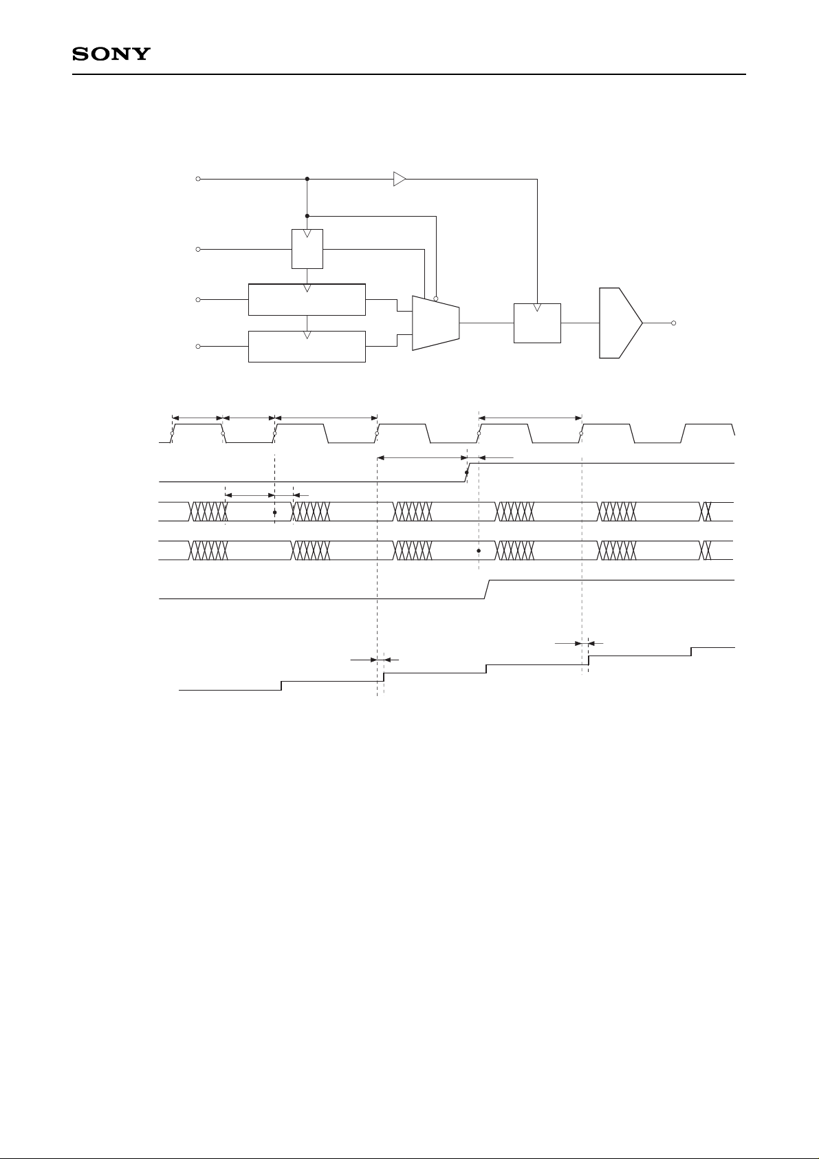
Block Diagram & Timing Chart (MUX.2 Mode)
th
Latch
Latch
Input Latch B
LatchInput Latch A
D
Q
Q
DACMUX
R
CLK/2
(Internal)
Analog out
Input Data A
Input Data B
DIV2IN
CLK
th-DIV
0 1
CLK
Input Data A
Input Data B
N
N + 1
N – 1 N +1 N + 3 N + 5 N + 7
N – 2 N N + 2 N + 4 N + 6
ts-DIV
tdo
N + 9
N + 8
N + 2
N + 3
N + 4
N + 5
Tpw1Tpw0
t
PD (A)
ts
DIV2IN
2 3
tPD (B)
tdo
In MUX.2 mode, the 1/2 frequency-divided clock signal (DIV2IN) and Data A and Data B, which are
synchronized with DIV2IN, are provided simultaneously. These signals are internally multiplexed and the
resulting signal can be analog output.
Page 26
– 26 –
CXA3197R
Block Diagram & Timing Chart (SELE.A, SELE.B Mode)
Latch
Input Latch B
Input Latch A
DAC Analog out
Input Data A
Input Data B
C2
CLK
Input Data A
Input Data B
N
N – 1 N +1 N + 3 N + 5 N + 7
N – 2 N N + 2 N + 4 N + 6
tdo
N + 9
N + 8
SELE. B
N + 2
N + 5
CLK
N + 7
N – 2
N – 4
SELE. A
ts th
ts-C2
th-C2
C2
C2 Latch OUT
Latch
Select
tPD (A)Tpw1 Tpw0 tPD (B)
tdo
1
0 1
0
In SELE.A and SELE.B modes, input Data A or Data B is selected and the selected data can be analog output.
When C1 = 1 and C3 = 0, Data A is selected for C2 = 0, and Data B is selected for C2 = 1.
Page 27

– 27 –
CXA3197R
Application Circuit
The circuit shown below is the basic circuit when the analog output is terminated with external resistance of 50Ω
for operation with dual ±5V power supply in MUX.2 mode. The analog output uses AVCCO as the reference.
The analog output full-scale voltage VFS is obtained with the following equation.
VFS = × (15 + ) × R R = RO//RL
RO: Output impedance (= 50Ω)
RL: External termination resistance
Here, VSET = VREF
(VREF ≈ 1.2V)
(R1 + R2 ≥ 1.2kΩ)
VSET
375
R2
R1 + R2
63
64
0V(D)
0V(A)
+5V(D)
–5V(A)
0V(A)
–5V(A)
R1 R2
–5V(A)
0V(A)
0V(A)
RL
0V(A)
0V(D)
–5V(D)
0V(D)
130
130
82
82
+5V(D)
VBB
2
3
4
5
6
7
8
9
10
11
12
1
DA5
DA4
DA3
DA2
DA1
DA0 (LSB)
DB9 (MSB)
DB8
DB7
DB6
DB5
DB4
25
26
27
28
29
30
36
35
34
31
32
33
AV
CC2
VSET
VREF
AGND2
AOUTP
AV
CCO
AOUTN
DV
CC2
C3
C2
C1
DGND2
DB3
DB2
DB1
DB0 (LSB)
DIV2IN
DIV2OUT
CLK/T
CLKP/E
CLKN/E
RESET/T
RESETP/E
RESETN/E
DA6
DA7
DA8
(MSB) DA9
DGND1
NC
DV
CC
1
PS
INV
R POLARITY
VOCLP
AGND2
40
39
38
37
41
42
43
44
45
46
47
48
13
14
15
16
17
18
19
20
21
22
23
24
TTL CLK/2
PECL CLK
DA0
to
DA9
DB0
to
DB9
RAM
·
Latch
·
etc
0V(A)
RL
Application circuits shown are typical examples illustrating the operation of the devices. Sony cannot assume responsibility for
any problems arising out of the use of these circuits or for any infringement of third party patent and other right due to same.
Page 28

– 28 –
CXA3197R
Notes on Use
• The CXA3197R has PECL and TTL input pins for the clock and reset inputs. When the clock is input at PECL
level, it is recommended to also input the reset signal at PECL level. Likewise, when the clock is input at TTL
level, it is recommended to also input the reset signal at TTL level.
• The input signal impedance should be properly matched to ensure the stable CXA3197R operation at high
speed.
Particularly when ringing appears in the input clock in the MUX.1A and MUX.1B modes, if this ringing
exceeds the clock input threshold value, the internal 1/2 frequency divider circuit may misoperate.
• All TTL input pins of the CXA3197R except for the PS pin go to High level when left open, and only the PS
pin goes to Low level when left open. Set the PS pin to High level to operate the IC.
When the PECL input pins are left open, the P (positive) side goes to High level and the N (negative) side
goes to Low level. The PECL input pins are complementary, so be sure to use the P and N sides together.
• When the clock and reset input signal level is TTL, ∗∗∗/T pins should be used and ∗∗∗/E pins left open. When
the clock and reset input signal level is PECL, ∗∗∗/E pins should be used and ∗∗∗/T pins left open.
• The power supply and grounding have a profound influence on converter characteristics. The power supply
and grounding method are particularly important during high-speed operation.
General points for caution are as follows.
— The ground pattern should be as wide as possible. It is recommended to make the power supply and
ground wider at an inner layer using a multi-layer board.
To prevent a DC offset from being generated between the analog and digital power supply patterns, it is
recommended to connect the patterns at one point via a ferrite-bead filter, etc.
— When using the CXA3197R with a single power supply, connect DGND1 and DGND2 to a common digital
ground, and AGND2 to an analog ground. Also, DVCC1 and DVCC2 should use a common digital power
supply, and AVCC2 should be connected to an analog power supply. AVCCO serves as the analog output
reference, so while it does not need to share the analog power supply, it should be used within the range
that satisfies the analog output compliance voltage.
— When using the CXA3197R with dual power supply, connect DGND1 and DVCC2 to the digital ground, and
AVCC2 to the analog ground. DVCC1 uses a positive digital power supply (+5V, typ.), DGND2 uses a
negative digital power supply (–5V, typ.), and AGND2 uses a negative analog power supply (–5V, typ.).
Like when using a single power supply, the AVCCO pin can be used within the range that satisfies the
analog output compliance voltage. However, connecting it to the analog ground and using the analog
ground as the reference for the analog output is recommended.
— Ground the power supply pins as close to each pin as possible with a 0.1µF or more ceramic chip
capacitor.
When using a single power supply, connect DVCC1 and DVCC2 to the digital ground, and AVCC2 and
AVCCO to the analog ground.
When using dual power supply, connect DVCC1 and DGND2 to the digital ground, and AGND2 to the
analog ground. In this case, when using AVCCO within the range that satisfies the compliance voltage, be
sure to also connect the AVCCO pin to the analog ground using a ceramic chip capacitor.
• The CXA3197R is designed with an analog output impedance of 50Ω. The analog outputs are wired with a
characteristic impedance of 50Ω, and waveforms free of reflection can be obtained by terminating the analog
outputs with 50Ω. Even when using only one of either AOUTP or AOUTN, if one analog output is terminated
with 50Ω, be sure to also terminate the other analog output with 50Ω. (See the Application Circuit.)
Page 29
– 29 –
CXA3197R
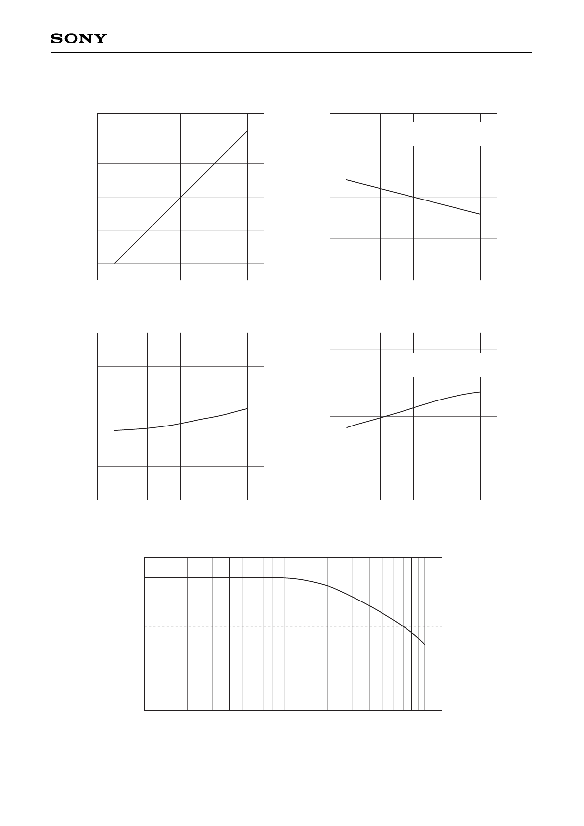
Example of Representative Characteristics
Output full-scale voltage vs. VSET pin voltage
Output full-scale voltage [mV]
VSET pin voltage [V]
R
L = 50Ω
1100
1000
900
800
700
0.65 0.84 1.03
Output full-scale voltage vs. Ambient temperature
V
FS
– Output full-scale voltage [mV]
Ta – Ambient temperature [°C]
1100
1050
1000
950
900
–25 25 750 50
VREF pin voltage vs. Ambient temperature
V
REF
pin voltage [mV]
Ta – Ambient temperature [°C]
1280
1260
1240
1220
–25 25 75
0 50
Output zero offset voltage vs. Ambient temperature
V
OF
– Output zero offset voltage [mV]
Ta – Ambient temperature [°C]
7
6
5
4
3
–25 25 75
0 50
Multiplying bandwidth
Analog output amplitude [dB]
VSET pin input frequency [MHz]
0
–3
1 10 100
RL = 50Ω
VSET = AGND2 + 937.5mW
RL = 50Ω
VSET = AGND2 + 937.5mW
Page 30
– 30 –
CXA3197R
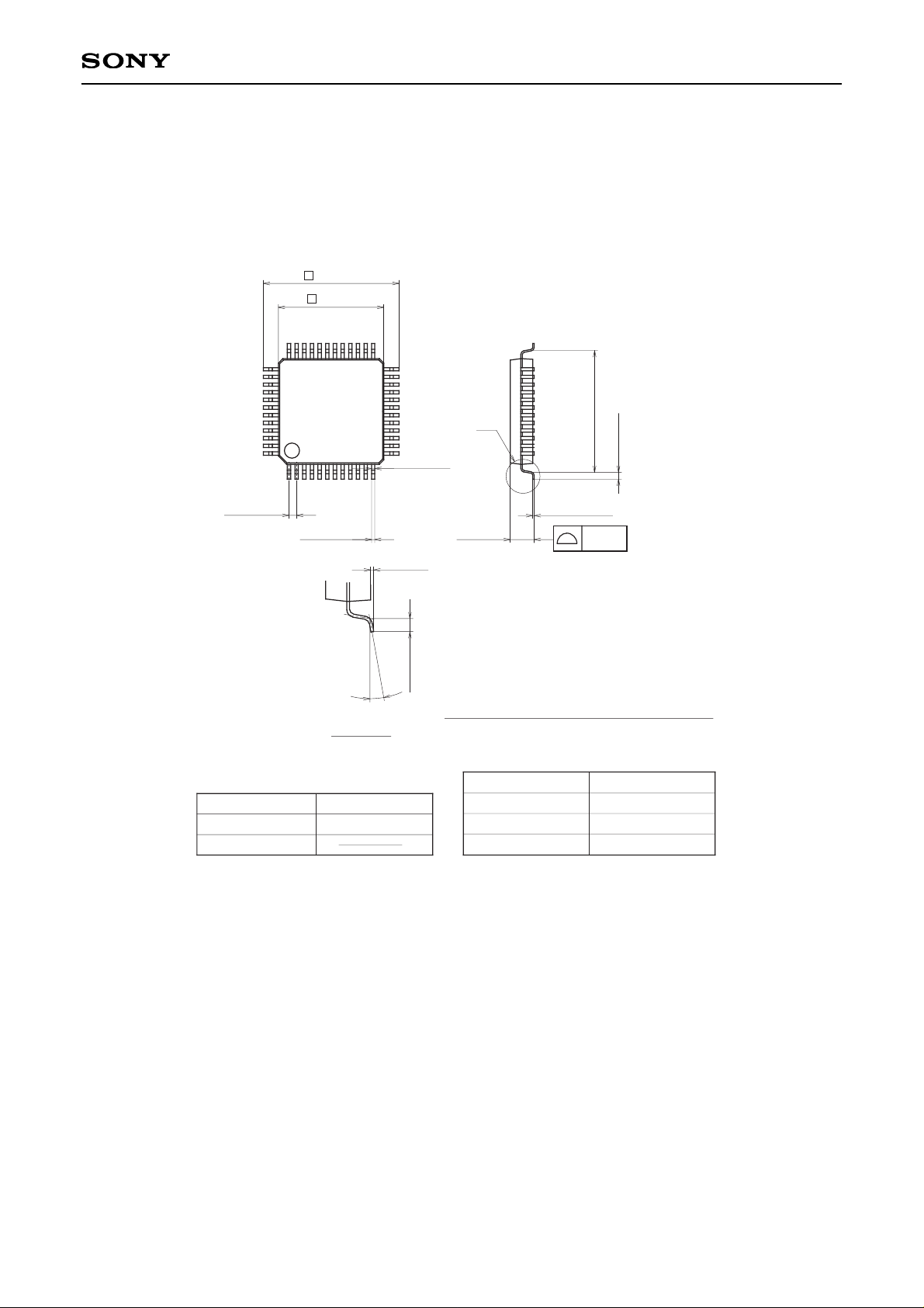
Package Outline Unit: mm
SONY CODE
EIAJ CODE
JEDEC CODE
PACKAGE MATERIAL
LEAD TREATMENT
LEAD MATERIAL
PACKAGE MASS
EPOXY RESIN
PLATING
42/COPPER ALLOY
PACKAGE STRUCTURE
48PIN LQFP (PLASTIC)
9.0 ± 0.2
∗ 7.0 ± 0.1
1
12
13
24
25
36
37
48
(0.22)
0.18 – 0.03
+ 0.08
0.5 ± 0.08
(8.0)
0.5 ± 0.2
0.127 – 0.02
+ 0.05
0.1 ± 0.1
0.5 ± 0.2
A
1.5 – 0.1
+ 0.2
0° to 10°
DETAIL A
0.2g
LQFP-48P-L01
LQFP048-P-0707
0.1
SOLDER/PALLADIUM
NOTE: Dimension “∗” does not include mold protrusion.
NOTE : PALLADIUM PLATING
This product uses S-PdPPF (Sony Spec.-Palladium Pre-Plated Lead Frame).
 Loading...