

Page 1
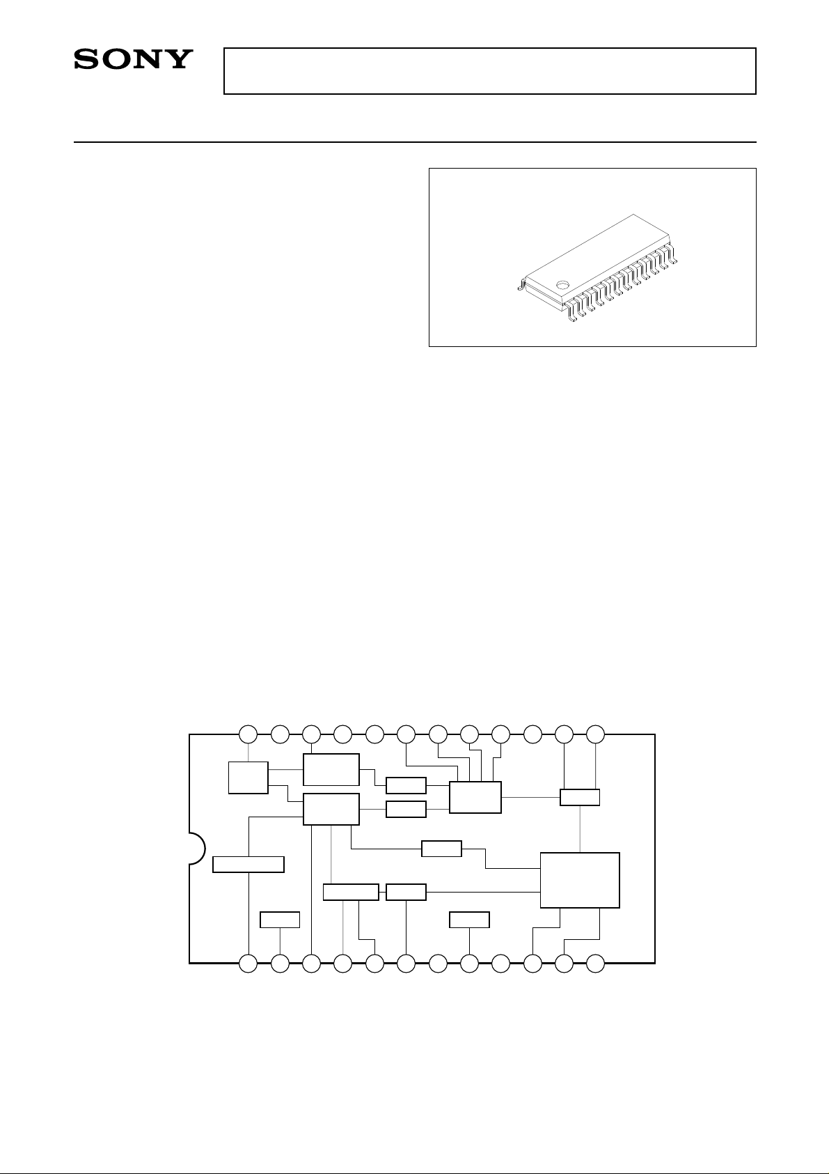
NICAM and SMATV RF MODULATOR/PLL
Description
Fully synthesized I2C controlled UHF/VHF TV RF
Modulator compatible with PAL and NTSC video
formats.
Features
• Minimal adjustment of external components
• For use on VHF and UHF TV Frequencies
• Video RF carrier frequency programmable in 125kHz
steps
• Accepts NICAM 6.552MHz QPSK input signal
• Accepts FM Stereo input signal
• I2C control of:
a. Video RF Carrier Frequency
b. Sound Carrier Frequency
c. Modulation Depth (±2% Typ.)
d. FM Deviation (±8% Typ.)
e. P/S ratio (±1dB Typ.)
f. Nicam output enable to sleep
g. Video RF carrier enable to sleep
• On chip Regulator 3.1V
Block Diagram
Structure
Bipolar silicon monolithic IC
Applications
• PAL and NTSC System VCR
• Satellite Receiver
• Set Top Box
• SMATV
Recommended Operating Voltages (Ta = 25°C)
• Supply voltage VCC 5.0 ± 0.5 V
• Supply for VCO Varactor 30 ± 0.5 V
• Operating Temperature –10 to +80 °C
CXA3050M
24 pin SOP (Plastic)
CC
CC
Analog GND
NICAM-in
NICAM
MIXER
VIDEO
MIXER
FM-OSC
3
Mod-adj
Analog V
21
4
Audio-in
20
RF-OUT
23
24
AMP
W/C-CLAMP
1
Video-in
Sony reserves the right to change products and specifications without prior notice. This information does not convey any license by
any implication or otherwise under any patents or other right. Application circuits shown, if any, are typical examples illustrating the
operation of the devices. Sony cannot assume responsibility for any problems arising out of the use of these circuits.
22
2
Vreg
OSC V
AMP
AMP
PLL
5
FM-Tank
OSC4
19
18
TPSG
6
7
filter
Audio-Loop
OSC3
17
VCO
OSCREG
Digital GND
OSC2
8
Xtal
OSC1
16
9
CC
Digital-V
OSC GND
15
2
I
10
SCL
14
C-Interface
11
PDout
PLL
PLL
SDA
EF
13
12
NC
– 1 –
E96331A66-ST
Page 2

Ground
A
RF Output
CXA3050M
B
C
A
D
B
Loop filter
XTAL
4MHz
Digital
Analog Digital
SMATV
Audio
Loop
Audio
CC
V
VCC Ground
Nicam in
Tank
Filter
NICAM
Mixer
P/S
control
PLL
FM Mod
RF Amp
and
Mixer
B62.5kHz
Adder
OSC
× 2
Buffer
depth
Modulation
8
divide
Loop
Filter
OSC
4MHz
25
divide
Phase
detector
M
divide
A
B
250kHz
62.5kHz
Regulator
Fig. 1
V Reg
Switch Amp
Audio in
NTSC
Multi-standard RF Modulator
Audio in
PAL
Modulation
depth
video
limiter
Video
clamp
Video in
– 2 –
Memory
2
SDA
CCT
Latch
C
I
B 4MHz
SCL
Page 3

CXA3050M
Functional Description of RF Modulator System
A block diagram of the RF modulator is shown in Fig. 1.
The composite video signal passes through an amplitude limiting circuit and a digitally controlled modulation
depth adjustment circuit. By means of three allocated I2C control bits it is possible to adjust the modulation
depth from a nominal 74% to 86% in 2.0% steps. Modulation depth can also be controlled externally by
addition of an external resistor on pin3. The video signal is then passed through to the mixer. In the mixer
stage, both the video composite signal and FM sound carrier amplitude modulate the RF carrier from the UHF
OSC, and the issuing signal is fed to the output via an RF amplifier.
The audio signals enter the chip via pin4. The FM Voltage Controlled Oscillator is band-switched to the
approximate centre frequencies of the four sound carrier frequencies 4.5MHz (NTSC) or 5.5, 6.0, 6.5MHz
(PAL). The required correct audio carrier frequency is fine tuned by the adjustment of fsound via I2C, where
upon the FM phase locked loop will lock the VCO onto the exact centre frequency. Minimum distortion of the
FM signal occurs when the centre frequency of the oscillator coincides with a mid-rail control voltage
(to 2.0V). Hence fine adjustment capacitors are also integrated on the chip, which tag into account any
capacitance variations from one batch to another. This is achieved by fine adjustment of Delta fsound via I2C
control. The design of the FM modulator eliminates the need for an external varactor.
The amplitude of the FM signal is varied via I2C by a digitally controlled logarithmic gain stage, which controls
the picture to sound power ratio (P/S). This signal is then fed into the RF amp. Hence at the RF output the P/S
ratio can be programmed in 1dB steps between the range 10dB and 17dB (see Electrical Characteristics).
Audio sensitivity can be programmed in 8% steps between the range –32% and +24%.
The UHF is phase locked to the reference frequency by means of the UHF phase locked loop. The VCO
output passes through a prescaler (≈8) followed by an I2C controlled programmable divider (≈M), and then
phase compared with that of a reference signal at 15.625kHz. The reference signal is derived from a 4MHz
crystal oscillator feeding a –256 divider. The UHF oscillator covers the frequency range 471MHz to 855MHz in
frequency steps of 125kHz. This is adequate for the UHF NTSC and PAL TV channels (471.25MHz (CH21) to
855.25MHz (CH69)). By adjustment of the external components around the oscillator and some adjustment to
output matching the RF modulator can also achieve range of frequencies in the VHF range.
The Nicam input (pin 22) accepts the 6.522MHz Nicam signal subcarrier QPSK at 728K bits/s data. This is
then buffered and feed into a separate mixer (controlled via VCO). This then feeds to the RF amp with the
composite video and audio. The I2C control will switch the Nicam signal output off or on.
– 3 –
Page 4

I2C Interface Data Format
CXA3050M
Modulator Address
Data 1
Data 2
Data 3
Data 4
1100100R/Wask
PD
M12
M4
X
Sound Carrier Course Adjust
S1
0
0
1
1
S0
0
1
0
1
Sound Carrier
Frequency
4.5MHz
5.5MHz
6.0MHz
6.5MHz
Sound Carrier Fine Adjust
ADJ1
M11
M3
NIC
TV System
(Pre-emphasis)
ADJ0
M10
M2
FM2
NTSC
PAL
PAL
PAL
S1
M9
M1
FM1
S0
M8
M0
FM0
over
mod
M7
MD2
PS2
X
M6
MD1
PS1
X
M5
MD0
PS0
ask
ask
ask
ask
ADJ1
0
0
1
1
ADJ0
0
1
0
1
df Adjust
–f
Normal
+f
+f
on chip
capacitance
6.4pF
3.2pF
1.6pF
0
PD RF Power on (RF Amp & OSC) 1 bit
OVM Over Modulation Test 1 bit
M12–MO Main divider control data 13 bits
S1–S0 Sound carrier frequency selection 2 bits
ADJ1–ADJ0 Sound carrier frequency adjust (0 to 6.4RF) 2 bits
MD2–MD0 Modulation Depth 3 bits
PS2–PS0 Picture/Sound control 3 bits
FM FM deviation adjust 3 bits
NIC Nicam Enable 1 bit
M12 MO Main UHF PLL Divider
MSB LSB 8191 to 2
Video Carrier frequency calculated from = 125 (M + 2) kHz
– 4 –
Page 5
CXA3050M
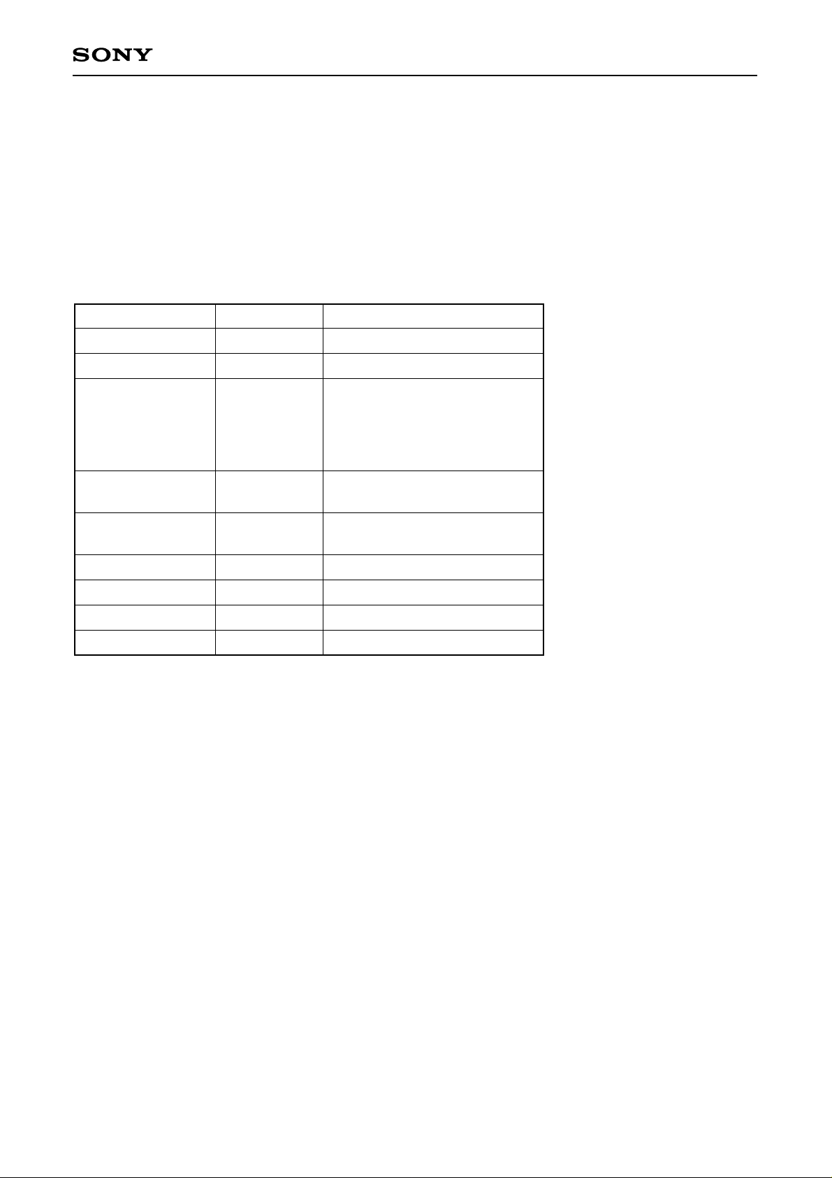
Software Application Notes
The minimum requirement to drive the CXA3050 and I2C bus drive is a 386/486 with 4M bytes hard disk
space, 16MHz clock speed and running DOS5.00 or above. Insert the disc into the drive and type TESTS and
at the prompt type iic. At this there should appear a single list of user friendly functional tests that can be
changed by keyboard manipulation. As an aid the test list is written below. Note Page up increments the
status, page down decrements the status.
Function Nominal Status
RF Output Power
Delta Sound
Fsound
Frequency mode
Mod depth
FM Deviation
P/S Ratio
Nicam on/off
Over Mod on/off
1/0
1
0
2 to 8191
4
4
4
1/0
1/0
Comments
Turns RF Amp, OSC on/off
Fine tune audio carrier
Course adjust for
4.5MHz (0)
5.5MHz (1)
6.0MHz (2)
6.5MHz (3)
Check listing on page 10 for
frequency to hex conversation
Ranges mod depth from
72% to 86%, 80% (4)
Sensitivity adjustable
Programmable in 8 steps of 1dB
Nicam Mixer on
Increase Video modulation ratio
– 5 –
Page 6

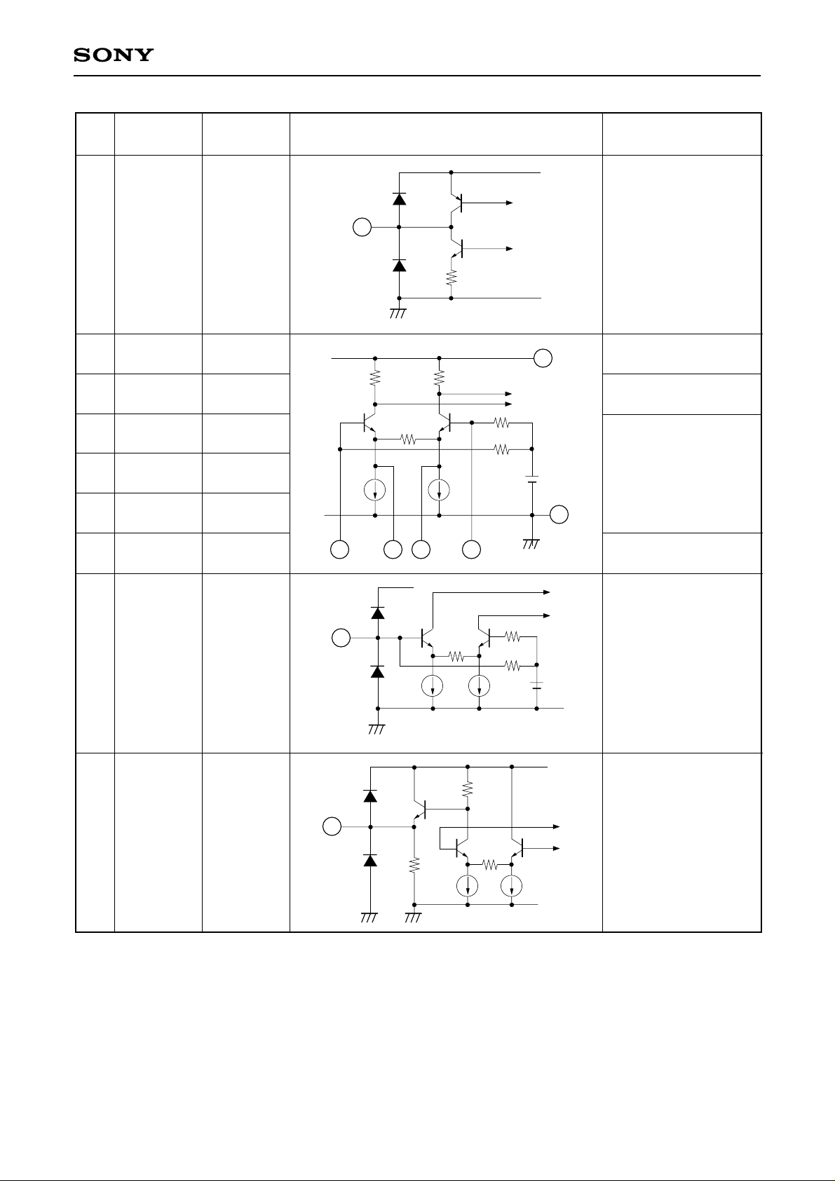
Pin Description
CXA3050M
Pin
No.
1
2
Reference
Video-in
Vreg
Pin Voltage
Typical DC
2.5V
3.1V
Equivalent circuit Description
Vcc
1
Vcc
2
Video input
Chip voltage supply
regulator
3
4
Mod-Adj
Audio-in
2.5V
10mA
MIXER
3
FMOSC
External Adjust Mod
depth.
Audio input
4
5
FM-Tank
4.0V
5
Sound Carrier
oscillator tank
– 6 –
Page 7

CXA3050M
Pin
No.
6
8
Reference
AudioLoop filter
Xtal
Pin Voltage
Typical DC
2.02V
1.5V
Equivalent circuit Description
Vcc
6
Sound Carrier FM tank
loop filter. See page 2
for set up note
Vcc
4MHz input crystal
frequency
8
10
11
13
SCL
SDA
EF
5/0 V
5/0 V
0.7V
10
11
13
I2C Clocking signal
input
I2C Data signal input
Charge pump output
– 7 –
Page 8
CXA3050M
Pin
No.
14
15
16
17
18
19
Reference
PDout
OSC GND
OSC1
OSC2
OSC3
OSC4
Pin Voltage
Typical DC
2.1V
0V
2.5V
1.7V
1.7V
2.5V
Equivalent circuit Description
14
Phase detector
output
20
VCO Ground
UHF OSC
15
20
22
24
OSC VCC
Nicam-in
RF-OUT
5V
2V
3.4V
24
19
22
18
17
16
MIXER
Oscillator supply
Voltage 5V
NICAM or FM
carrier input
RF output.
Must be terminated
with 75Ω.
Application Circuit Notes
1. RF output pin 24 should be connected to a 75Ω load in oder to measure accurate input level. Also note pin 24
has 2.7kΩ to GND.
The output is measured using a spectrum analyzer.
2. After turning the device on, tune the variable inductor FM Tank so at the 6.5MHz setting (set by I2C control)
the voltage on pin 6 should read 2.02V.
Set Fsound = 3
Delta Fsound = 1
– 8 –
Page 9

Specifications
CXA3050M
Parameter
Operating temperature range
Modulation Index
Diff. Gain 80 to 87.5% modulation
Diff. Gain 80 to 87.5% modulation
Deviation range (audio)
NICAM input level
NICAM input resistance
Picture/sound ratio adj
Video modulation adj
Audio FM sensitivity
Picture/Sound ratio
Inter carrier accuracy
Parameter
Current consumption
Full operation
VCC = 5.0V
New Specification
–10 to 80°C
77.5 to 90%
±6.5 degree
±10kHz to ±100kHz
79dBµV
1dB × 7steps
2% × 7steps
8% × 7steps
1dB × 7steps
Condition
Analog
digital
OSC
±6.5%
1kΩ
±1kHz
Min.
40
20
9.6
Typ.
50
25
12
Max. Unit
61.3
30.6
14.6
mA
mA
mA
DC Supply operating range
Operating temperature range
Input level
Output level
Input resistance
Bit error rate
Eye-height degradation
Conversion, Loss = 30dB
4.5
–10
–20
5.0
79
–22
10e
7
75
Vdc
°C
dBµV
–24
1
–9
10e
10
dBc
KΩ
–6
%
– 9 –
Page 10
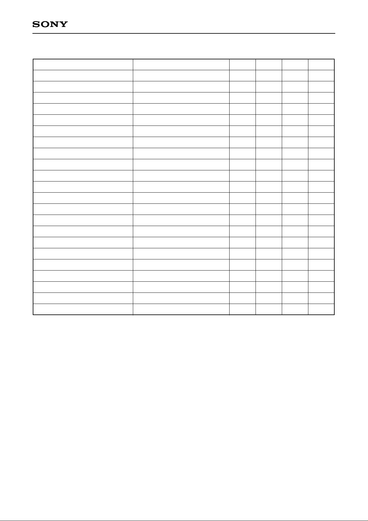
RF Characteristics
CXA3050M
Parameter
Output impedance
Output return loss
RF Output level
RF Frequency respone
Picture/Sound ratio
VHF1 Frequency range
VHF2 Frequency range
UHF Frequency range 1
UHF Frequency range 2
RF Accuracy
Inter-carrier frequency range
Inter-carrier accuracy
RF Carrier phase noise
Sound carrier phase noise
Hum modulation
Chroma beat
Condition
700MHz 75Ω termination
Using attached application
Using attached application
4.5, 5.5, 6.0, 6.5
4.5, 5.5, 6.0, 6.5
10kHz offset frequency
10kHz offset frequency
Min.
–7
10
50
170
470
670
4.5
0
Typ.
75
79
–84.7
–84.7
–78
Max. Unit
Ω
dB
±2.5
±1
17
120
230
860
800
±50
6.5
±1
–80
–80
–60
–65
dBµV
dB
dBc
MHz
MHz
MHz
MHz
kHz
MHz
kHz
dBc/Hz
dBc/Hz
dB
dBc
C/N Ratio
RF Harmonics
Sub-carrier harmonics
NICAM Beat
Reference spurious frequency.
Spurious output level
1/2 Video band offset
15.625kHz
–63
–60
–60
–15
–60
–65
–55
–65
dB
dBc
dBc
dBc
dBc
dBc
– 10 –
Page 11
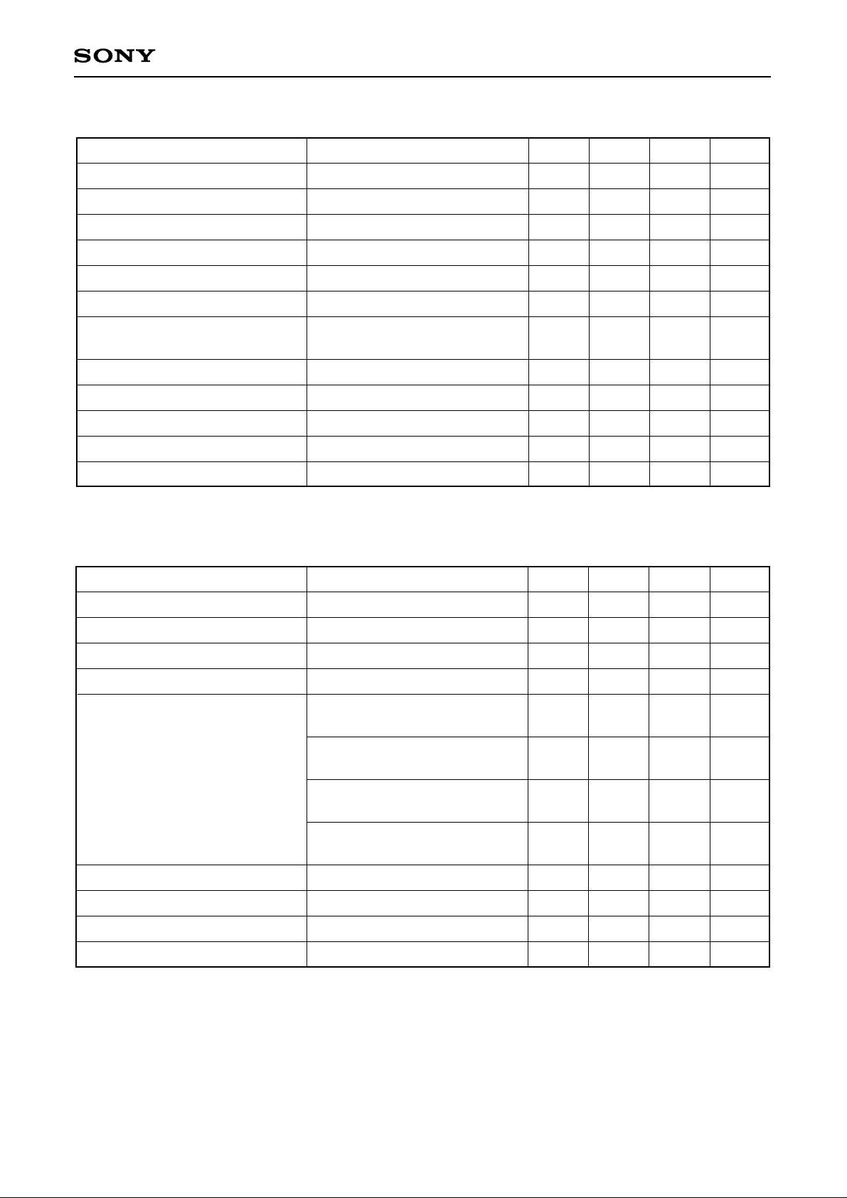
Video Characteristics
CXA3050M
Parameter
Input resistance
Input voltage
% Modulation Clipping
I2C control index
Modulation flatness
Modulation
Modulation stability by temperature
Field time distortion
Line time distortion
S/N
K Factor
Video frequency response
Audio Characteristics
Condition
80% Modulation
7 steps
Band Limited (46CH to 60CH)
0.55p-p input (mod Adja)
mp (Ta = –10 to 80°C)
–mp (Ta = 25°C)
Weighted
With 2T pulse
Per standard
Min.
30
73
0
0
0
Typ.
100
0.55
2
80
0.5
0.5
Max. Unit
KΩ
Vp-p
97
±0.4
±1.4
87
±3
2
2
–60
2
±0.5
%
%
%
%
%
IRE
IRE
dB
%
dB
Parameter
Input voltage
Input resistance
Deviation range
Audio distribution
Deviation sensitivity
Audio SNR
Harmonic distortion
Frequency response
FM Hum and noise
Condition
@50kHz, Deviation
4.5MHz
System M
4.5MHz ± 25kHz = 100% = 0dB
System B/G
5.5MHz ± 50kHz = 100% = 0dB
System I
6MHz ± 50kHz = 100% = 0dB
System D/K
6.5MHz ± 50kHz = 100% = 0dB
Quasi-Parallel, Detection
50 to 100%, Deviation
50 to 15kHz
25 to 75kHz, Deviation
Min.
0.1
20
±10
–1
Typ.
0
0.5
0.33
0.404
0.404
Max. Unit
Vp-p
KΩ
±100
±15
kHz
%
kHz/mV
kHz/mV
kHz/mV
kHz/mV
–60
1
+1
±5
dB
%
dB
kHz
– 11 –
Page 12
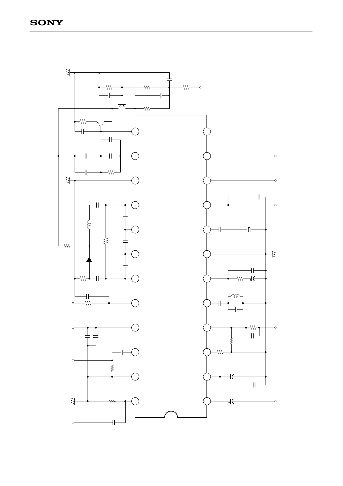
GND
R12
300
C27
R16
20pF
56k
P1
R152kC28
200
R13
C26
1nF
1nF
R14
CXA3050M
200
+30V
GND
R9
CC VCC
V
C25
20k
OSC
Analog
C7
1nF
R8
1nF
C23
C21
20k
C11
22pF
R6
0.047µF
1nF
10
C19
L2
25nH
330
R10
1T363
C13
Q1
220pF
220pF
C6
22pF
75
R2
C24
C22
C18
C16
C14
0.01µF
1nF
6pF
2pF
6pF
C5
R11
1nF
20k
13
14
15
16
17
18
19
20
21
22
23
EF
CC
PDOUT
OSC1
OSC2
VCO3
OSC4
OSC-V
A-GND
OSC-GND
ANALOG-V
NICAM-IN
NC
SDA
SCL
D-V
CC
XTAL
D-GND
ALF
TANK
AUDIO
MOD-ADJ
VREG
12
11
10
9
8
7
6
5
4
3
2
C17
C10
R4
R3
27pF
L1
0.01µF
22k
100k
17µH
C4
C9
R7
22pF
22µF
240
C20
0.1µF
4MHz-Xtal
C15
22nF
C12
47µF
R5
180k
C8
330pF
VCC SCL SDA
GND
AUDIOVIDEO
Application circuits shown are typical examples illustrating the operation of the devices. Sony cannot assume responsibility for
any problems arising out of the use of these circuits or for any infringement of third party patent and other right due to same.
RF OUT GND NICAM
Application Circuit 1
R1
C1
2.7k
22pF
24
RFOUT
– 12 –
VIDEO
1
C2
C3
22pF
0.33µF
Page 13
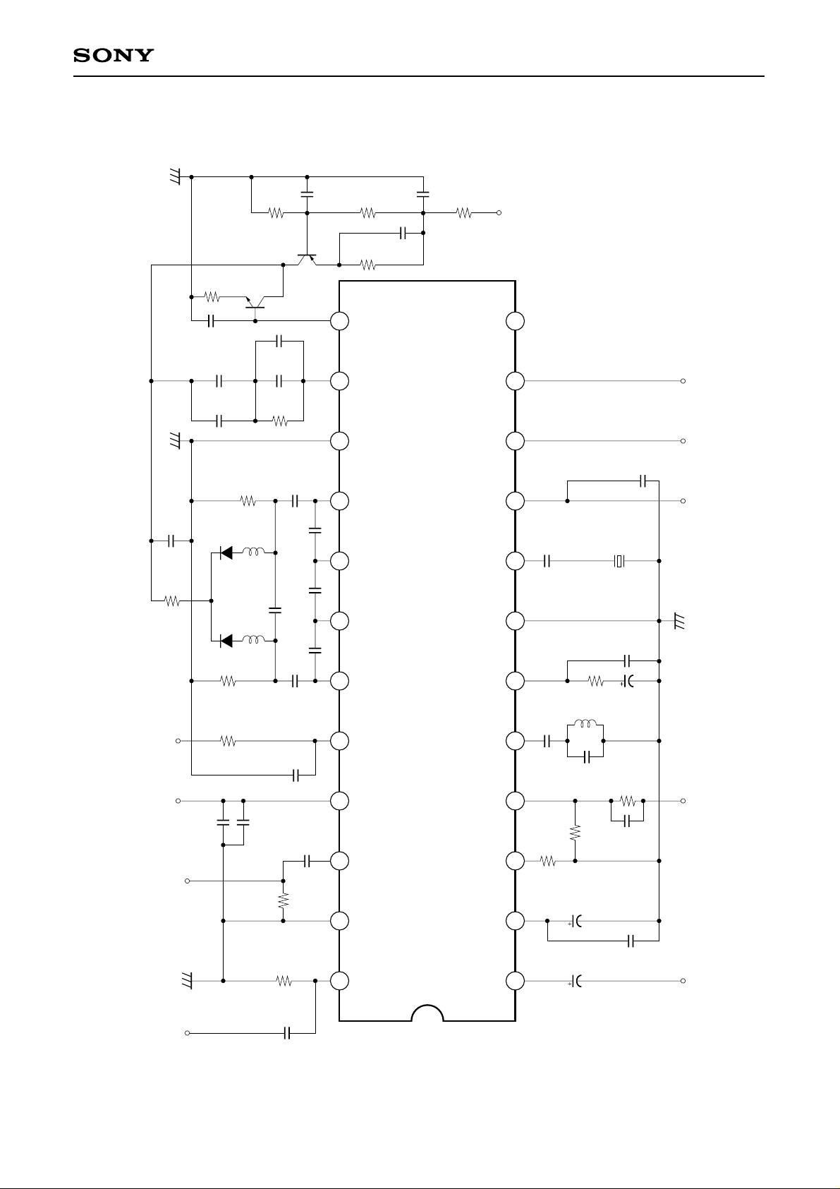
GND
R12
300
R16
56k
C29
P1
20pF
R152kC28
200
R13
C27
1nF
1nF
R14
CXA3050M
200
+30V
CC VCC
V
GND
C30
220pF
R9
20k
L = 14nH
Analog OSC
C26
C7
1nF
C24
C22
1T363
1nF
0.047µF
1nF
R10
1T363
R8
20k
10
R6
L3
C16
L2
20k
14nH
5pF
14nH
C6
R2
Q1
C25
C23
22pF
75
0.01µF
1nF
C20
C19
C17
C14
C13
C9
220pF
6pF
3pF
6pF
220pF
22pF
C5
R11
1nF
20k
13
14
15
16
17
18
19
20
21
22
23
CC
EF
PDOUT
OSC1
OSC2
VCO3
OSC4
OSC-V
A-GND
OSC-GND
ANALOG-V
NICAM-IN
NC
SDA
SCL
D-V
CC
XTAL
D-GND
ALF
TANK
AUDIO
MOD-ADJ
VREG
12
11
10
9
8
7
6
5
4
3
2
C18
C11
R4
R3
27pF
L1
0.01µF
22k
100k
17µH
C4
C10
R7
22pF
22µF
240
C21
0.1µF
4MHz-Xtal
C15
22nF
C12
47µF
R5
180k
C8
330pF
VCC SCL SDA
GND
AUDIOVIDEO
Application circuits shown are typical examples illustrating the operation of the devices. Sony cannot assume responsibility for
any problems arising out of the use of these circuits or for any infringement of third party patent and other right due to same.
RF OUT GND NICAM
Application Circuit 2
Dual-OSC
R1
C1
2.7k
22pF
24
RFOUT
– 13 –
VIDEO
1
C2
C3
22pF
0.33µF
Page 14

CXA3050M
GND
GND
C19
R10
CC VCC
V
C26
1nF
20k
OSC
Analog
C7
R12
1nF
R8
1nF
300
C24
C22
20k
C11
R6
0.047µF
1nF
C20
L2
R9
1T363
22pF
10
1µH
510
C13
R2
Q1
C25
C23
330pF
330pF
C6
22pF
75
0.01µF
1nF
C18
C16
C14
R11
120pF
47pF
120pF
C5
1nF
20k
R16
13
14
15
16
17
18
19
20
21
22
23
56k
CC
EF
C29
P1
PDOUT
OSC1
OSC2
VCO3
OSC4
OSC-V
A-GND
R15
20pF
R13
OSC-GND
ANALOG-V
NICAM-IN
2k
200
C27
C28
1nF
SCL
CC
XTAL
ALF
AUDIO
VREG
1nF
NC
12
SDA
11
10
D-V
9
8
D-GND
7
6
TANK
5
4
MOD-ADJ
3
2
C17
C10
R4
R3
27pF
L1
0.01µF
22k
100k
R14
17µH
C4
200
C9
R7
22pF
22µF
240
+30V
C21
0.1µF
4MHz-Xtal
C15
22nF
C12
47µF
R5
180k
C8
330pF
VCC SCL SDA
GND
AUDIOVIDEO
Application circuits shown are typical examples illustrating the operation of the devices. Sony cannot assume responsibility for
any problems arising out of the use of these circuits or for any infringement of third party patent and other right due to same.
RF OUT GND NICAM
Application Circuit 3
VHF-Band
R1
C1
2.7k
22pF
24
RFOUT
– 14 –
VIDEO
1
C2
C3
22pF
0.33µF
Page 15
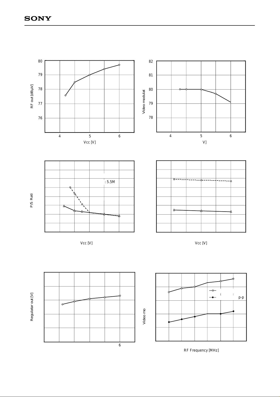
Example of Representative Characteristics
CXA3050M
80
79
78
77
RF out [dBµV]
76
20
19
18
17
16
P/S Ratio [dB]
15
14
Video modulation [%]
456
Vcc [V]
A : 4.5M
A
B
B : 5.5M
82
81
80
79
78
456
0.6
0.5
0.4
FM Sencitivity [kHz/mw]
0.3
Vcc [V]
3.3
3.2
3.1
3.0
Regulatar out [V]
2.9
456
Vcc [V]
Video modulation [%]
456
Vcc [V]
95
90
85
80
75
456
Vcc [V]
Video max.
Video 0.55Vp-p
600 700 800 900
RF Frequency [MHz]
– 15 –
Page 16
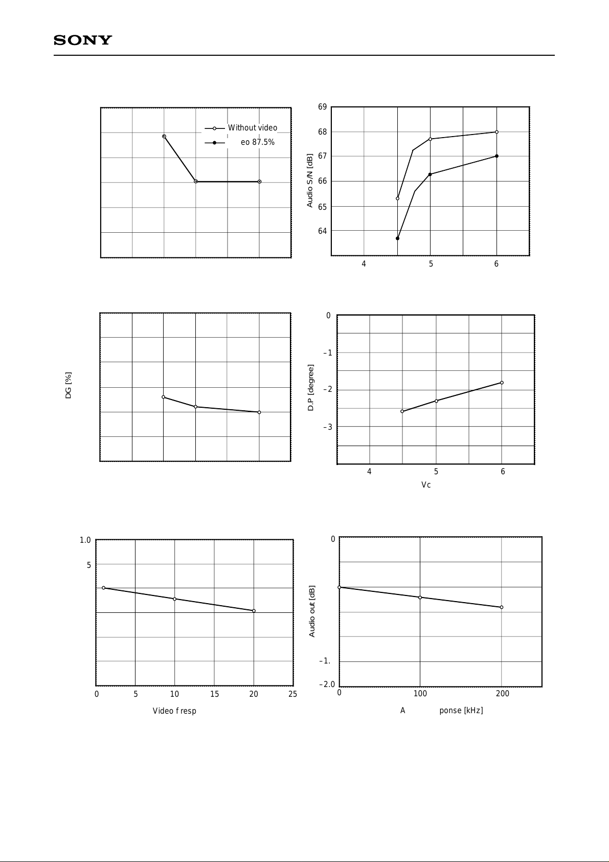
CXA3050M
A
A
A
A
A
A
0.40
0.35
0.30
0.25
Audio dist [%]
0.20
0.15
3.0
2.5
2.0
1.5
DG [%]
1.0
0.5
Without video
Video 87.5%
Audio S/N [dB]
456
Vcc [V]
D.P [degree]
69
68
67
66
65
64
456
Vcc [V]
0
–1
–2
–3
0
3.5 4 4.5 5 5.5 6 6.5
Vcc [V]
1.0
0.5
0
–0.5
Video out [dB]
–1.0
–1.5
–2.0
0 5 10 15 20 25
Video f response [MHz]
1.0
0.5
0
–0.5
Audio out [dB]
–1.0
–1.5
–2.0
0
456
Vcc [V]
100 200
Audio f response [kHz]
– 16 –
Page 17
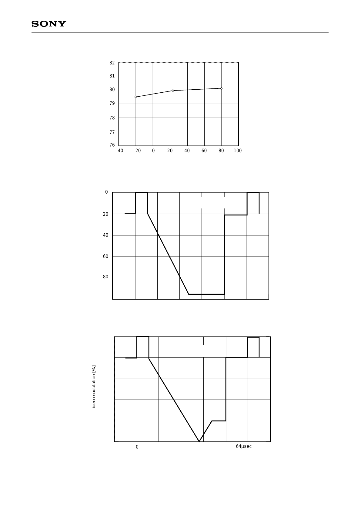
82
81
80
79
78
Video modulation [%]
77
76
–40 –20 0 20 40 60 80 100
Temperature [degree]
0
Over mod test = OFF
Video 0.8Vp-p
20
CXA3050M
40
60
Video modulation [%]
80
100
0
0
20
40
60
Video modulation [%]
64µsec
Over mod test = ON
Video 0.8Vp-p
80
100
0
64µsec
– 17 –
Page 18
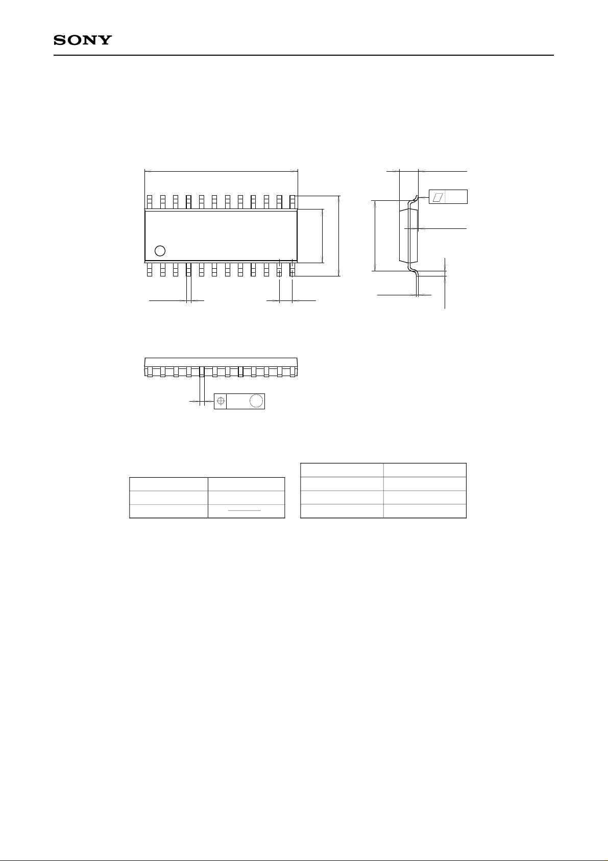
Package Outline Unit: mm
CXA3050M
24PIN SOP (PLASTIC)
+ 0.4
15.0 – 0.1
1324
+ 0.3
5.3 – 0.1
7.9 ± 0.4
112
1.270.45 ± 0.1
± 0.12
M
6.9
0.2 – 0.05
+ 0.1
PACKAGE STRUCTURE
SONY CODE
EIAJ CODE
JEDEC CODE
SOP-24P-L01
∗SOP024-P-0300-A
MOLDING COMPOUND
LEAD TREATMENT
LEAD MATERIAL
PACKAGE WEIGHT
EPOXY/PHENOL RESIN
SOLDER PLATING
COPPER ALLOY / 42ALLOY
0.3g
+ 0.4
1.85 – 0.15
0.15
+ 0.2
0.1 – 0.05
0.5 ± 0.2
– 18 –
 Loading...