

Page 1
– 1 –
CXA3071N
E96146B8Z
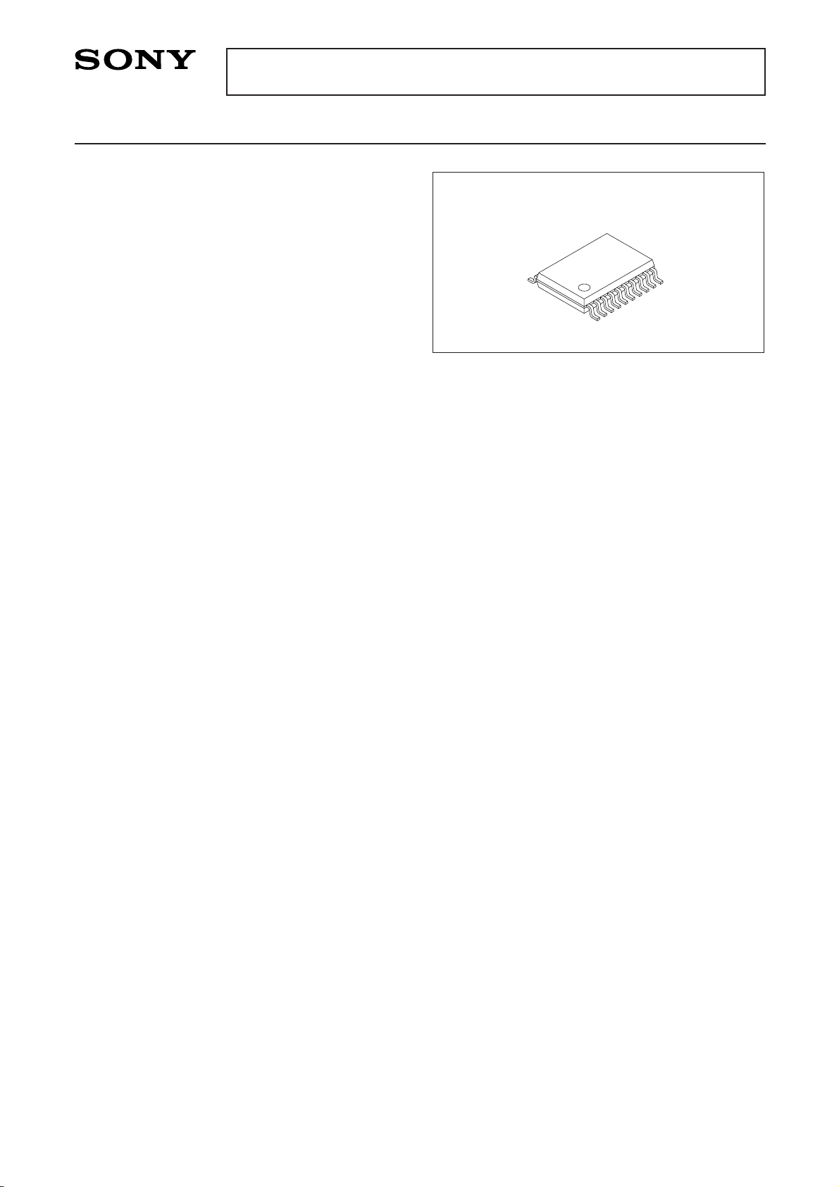
Read/Write Amplifier (with Built-in Filters) for FDDs
Description
The CXA3071N is a monolithic IC designed for use
with three-mode Floppy Disk Drives, and contains a
read circuit (with a four-mode filter system), a write
circuit, an erase circuit, and a supply voltage
detection circuit, all on a single chip.
Features
• Single 5V power supply
• All filter, write current and other characteristics can
be set with a single external resistor.
• Filter system can be switched among four modes:
1M, 1.6M/2M, which are each inner track/outer
track.
• Filter characteristics can be set to Chebyshev (1dB
ripple) for 1.6M, 2M/inner track only, and to
Butterworth for the other modes and a custom
selection can be made between Chebyshev (1dB
ripple) and Butterworth for 1.6M, 2M/inner track
only.
• 1M/outer track f0 and the fc ratio for each mode
can be customized.
• Preamplifier voltage gain can be set to 45dB or
48dB by switching the filter mode and inner/outer
track.
• Preamplifier and filter output are monitored with
the same pins. These pins are normally set to filter
output, but the preamplifier output can be
monitored by temporarily setting the SETR pin (Pin
20) to Low.
• Time domain filter can be switched between two
modes: 1M, 1.6M/2M.
In addition, the pulse width can be customized.
• Write current can be switched among six modes
according to the mode and inner/outer track
setting.
The current value can be customized for each
mode.
• Erase current remains constant, and the current
value can be customized.
• Damping resistor can be built in. Resistor can be
customized between 2kΩ and 15kΩ in 1kΩ steps.
• Supply voltage detection circuit
Applications
Three-mode FDDs
Structure
Bipolar silicon monolithic IC
Absolute Maximum Ratings (Ta = 25°C)
• Supply voltage VCC 7.0 V
• Digital signal input pin voltage
–0.5 to VCC + 0.3 V
• Power ON output applied voltage
VCC + 0.3 V
• Erase output applied voltage VCC + 0.3 V
• Write head applied voltage 15 V
• Power ON output current 7 mA
• Operating temperature Topr –20 to +75 °C
• Storage temperature Tstg –65 to +150 °C
• Allowable power dissipation
PD 375 mW
Operating Conditions
Supply voltage 4.4 to 6.0 V
Sony reserves the right to change products and specifications without prior notice. This information does not convey any license by
any implication or otherwise under any patents or other right. Application circuits shown, if any, are typical examples illustrating the
operation of the devices. Sony cannot assume responsibility for any problems arising out of the use of these circuits.
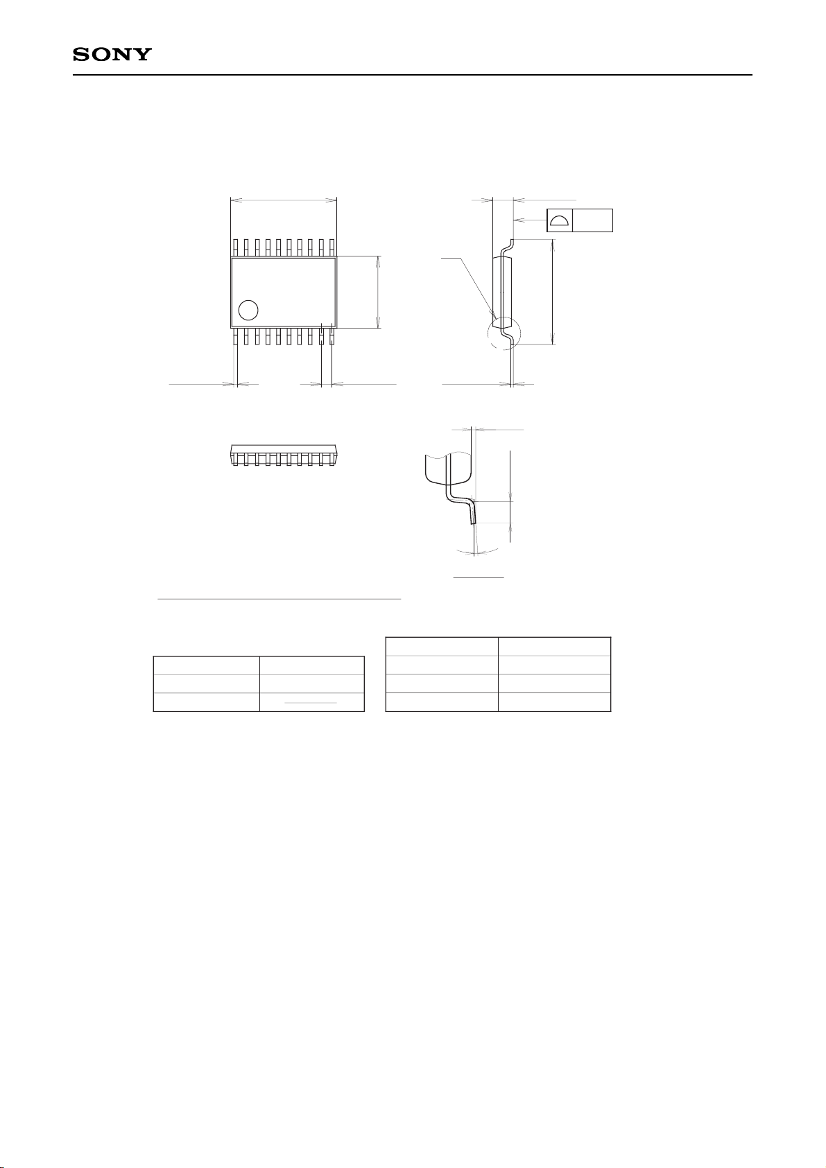
20 pin SSOP (Plastic)
For the availability of this product, please contact the sales office.
Page 2
– 2 –
CXA3071N
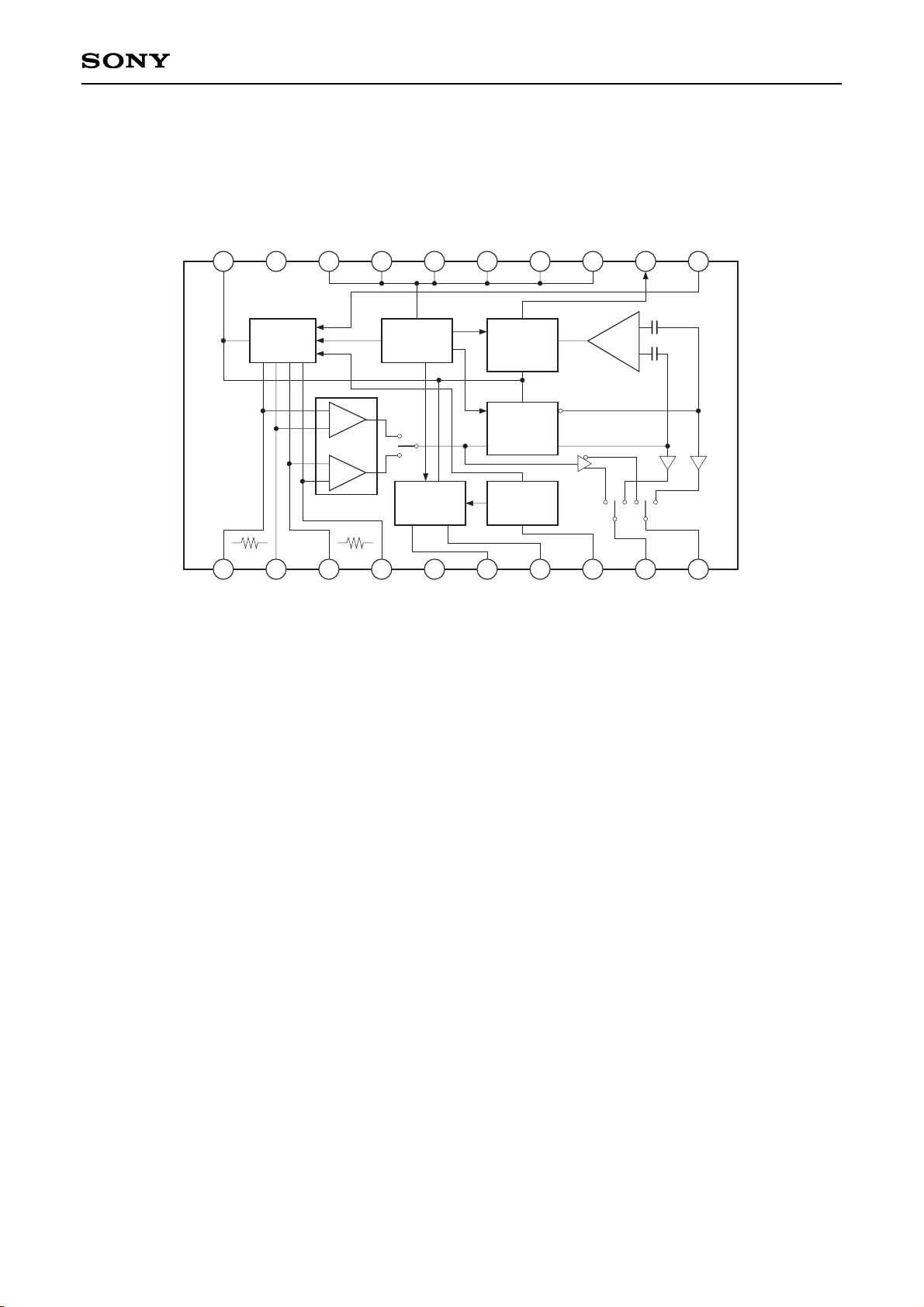
Block Diagram and Pin Configuration
WRITE
DRIVER
COMP
PREAMP
CONTROL
LOGIC
TIME
DOMAIN
FILTER
FILTER
DIFF + LPF
(BPF)
POWER
MONITOR
ERASE
DRIVER
2
3
4
5
6
7
8
9
10
1
11
12
13
14
15
16
17
18
19
20
HEAD1A
HEAD1B
HEAD0A
HEAD0B
GND
ERA0
ERA1
PONOUT
MONITORA
MONITORB
SETR
V
CC
X360
XHD
OTF
XS1
XEG
WG
RD
XWD
Page 3
– 3 –
CXA3071N
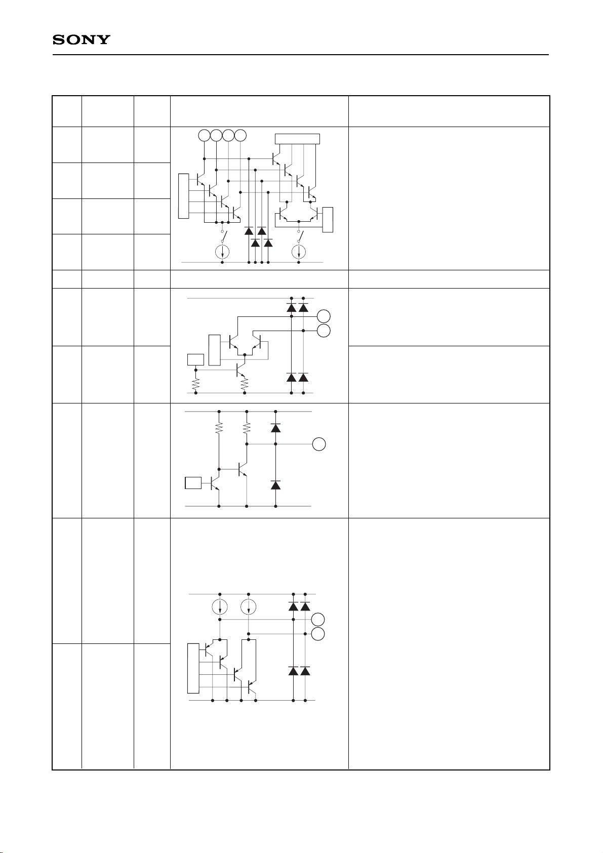
Pin Description
Pin
No.
Symbol
Pin
voltage
Equivalent circuit Description
1
2
3
4
HEAD1A
HEAD1B
HEAD0A
HEAD0B
—
—
—
—
Magnetic head inputs/outputs.
Connect the recording/playback magnetic
head to these pins, and connect the center
tap to V
CC. When the logical voltage for
Pin 15 (XS1) is Low, the HEAD1 system is
active; when the logical voltage is High,
the HEAD0 system is active.
GND
2
3
4
1
5
GND —
GND connection.
6 ERA0
—
7
ERA1
—
8
9
10
PON
OUT
—
MONITORA
4.0V
during
filter
output
3.4V
during
preamplifier
output
4.0V
during
filter
output
3.4V
during
preamplifier
output
MONITORB
Erase output for the HEAD0 system.
Erase output for the HEAD1 system.
Reduced voltage detection output. This is
an open collector that outputs a low signal
when VCC is below the specified value.
MONITOR differential outputs.
These pins are set to filter output during
normal read mode, but the preamplifier
output can be monitored by temporarily
setting Pin 20 (SETR) to Low.
VCC
GND
6
7
VCC
GND
8
100k 100k
500µ500µ
9
10
V
CC
GND
Page 4
– 4 –
CXA3071N
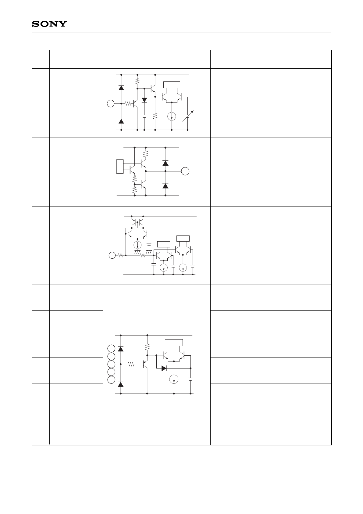
11 XWD —
Write data input. This pin is a Schmitttype input that is triggered when the
logical voltage goes from High to Low.
VCC
1k
GND
2.3V
11
140
V
CC
GND
12
GND
0.65
V
CC
0.35
VCC
13
147
VCC
0.5
VCC
VCC
100k
1k
GND
2.1V
14
15
16
17
18
12
13RDWG
—
0.5VCC
during
read
Read data output.
This pin is active when the logical voltage
of the write gate signal and the erase gate
signal is High.
WG signal input.
The write system becomes active when
the logical voltage is High.
The IC is in power saving mode when the
logical voltage is Low.
The read system becomes active when
the logical voltage is Z.
14
XEG
—
XEG signal input. The erase system
becomes active when the logical voltage
is Low.
15
XS1
—
16
OTF
—
—
—
Head side switching signal input. The
HEAD1 system is active when the logical
voltage is Low, and the HEAD0 system is
active when the logical voltage is High, but
only when the logical voltage for the WG
signal is Z and of the XEG signal is High.
Filter inner track/outer track mode control.
Outer track mode is selected when the
logical voltage is High.
Filter, time domain filter and write current
1M/2M mode control. 1.6M/2M mode is
selected when the logical voltage is Low.
17
18
19
XHD
X360
VCC
—
Filter, time domain filter and write current
1.6M/2M mode control. 1.6M mode is
selected when the logical voltage is Low.
Power supply (5V) connection.
Pin
No.
Symbol
Pin
voltage
Equivalent circuit Description
Page 5
– 5 –
CXA3071N
3.8V
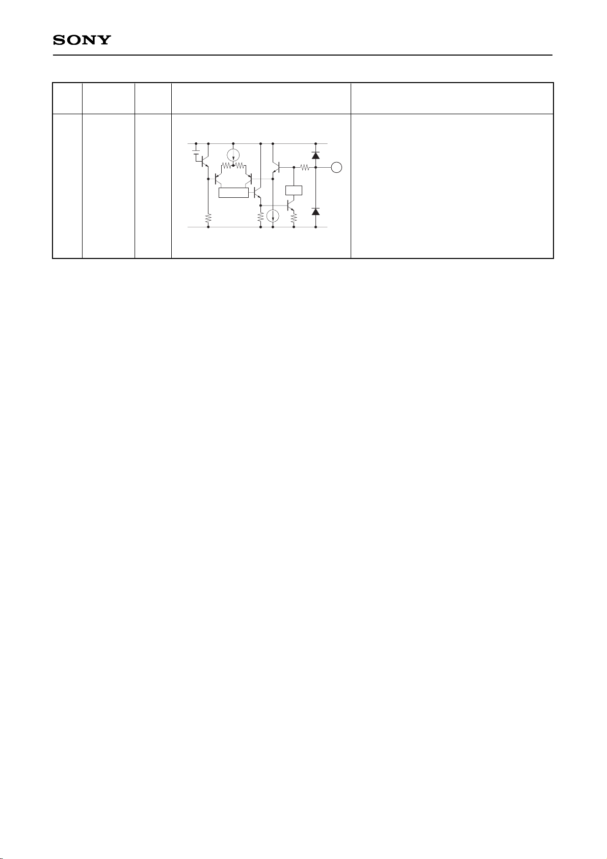
20 SETR
Filter cutoff frequency, time domain filter
1st monostable multivibrator pulse width,
read data, write current and erase current
setting resistor connection. Connect the
setting resistor R between this pin and
VCC.
Pin
No.
Symbol
Pin
voltage
Equivalent circuit Description
147
VCC
20
1.2V
GND
Page 6
– 6 –
CXA3071N
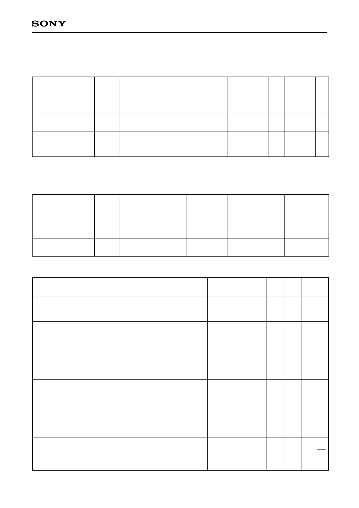
Electrical Characteristics
Current Consumption (Ta = 25°C, VCC = 5V)
Current consumption
in read mode
Current consumption
in write/erase mode
Current consumption
in power saving
mode
ICCR
ICCWE
ICCPS
WG = "Z"
WG = "H", XEG = "L"
WG = "L"
—
—
—
—
—
—
15.0
11.0
—
25.0
17.0
1.2
35.0
23.0
2.0
mA
mA
mA
Power Supply Monitoring System (Ta = 25°C)
Power supply
ON/OFF detector
threshold voltage
Power ON output
saturation voltage
VTH
VSP
VCC = 3.5V
I = 1mA
—
—
—
—
3.5—3.9—4.3
0.5VV
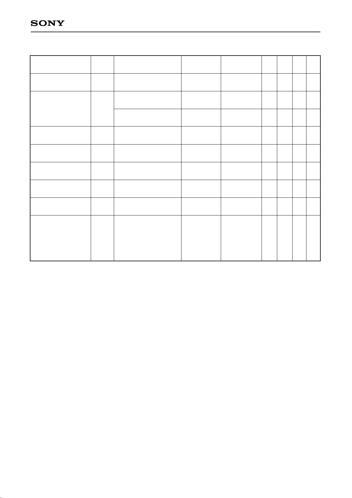
Read System (Ta = 25°C, VCC = 5V)
Preamplifier
voltage gain
1M/outer track
Preamplifier
voltage gain
1M/inner track
Preamplifier
voltage gain
1.6M, 2M/
outer track
Preamplifier
voltage gain
1.6M, 2M/
inner track
Preamplifier
frequency
response
Preamplifier
input
conversion
noise voltage
GVLO
GVLI
GVHO
GVHI
BWO
ENO
f = 100kHz, OTF = "H",
XHD = "H", X360 = "X"
f = 100kHz, OTF = "L",
XHD = "H", X360 = "X"
f = 100kHz, OTF = "H",
XHD = "L", X360 = "X"
f = 100kHz, OTF = "L",
XHD = "L", X360 = "X"
GV/GV0 = –3dB
BW = 400Hz to 1MHz,
VI = 0
1
1
1
1
1
1
A, B
A, B
A, B
A, B
A, B
A, B
43.1
46.1
43.1
46.1
5
—
45.0
48.0
45.0
48.0
—
2.0
46.6
49.6
46.6
49.6
—
2.9
dB
dB
dB
dB
MHz
nV/√Hz
Item Symbol
Conditions
Measurement
circuit
Measurement
point
Min. Typ. Max. Unit
Item Symbol
Conditions
Measurement
circuit
Measurement
point
Min. Typ. Max. Unit
Item Symbol
Conditions
Measurement
circuit
Measurement
point
Min. Typ. Max. Unit
Page 7
– 7 –
CXA3071N
Read System (Ta = 25°C, VCC = 5V)
Filter output voltage
amplitude
Time domain filter
monostable
multivibrator pulse
width
Read data pulse
width
Read data output low
output voltage
Read data output
high output voltage
Read data output
∗1
rise time
Read data output
∗1
fall time
Peak shift
∗2
VOF
T1
T2
VOL
VOH
tr
tf
PS
X360 = "X", XHD = "H"
(1M mode)
X360 = "X", XHD = "L"
(1.6M/2M mode)
IOL = 2mA
IOH = –0.4mA
RL = 2kΩ
CL = 20pF
RL = 2kΩ
CL = 20pF
VI = 0.25mVp-p to
3.5mVp-p
X360 = "H", XHD = "L"
OTF = "L"
f = 125kHz,
2M/inner track mode
1
1
1
1
1
1
1
1
1
A, B
C, D
C, D
D
D
D
D
D
D
1.4
2.25
1.16
300
—
2.8
—
—
—
—
2.50
1.29
400
—
—
—
—
—
—
2.75
1.42
500
0.5
—
100
100
1
Vp-p
µs
µs
ns
V
V
ns
ns
%
∗1
Read data output: 0.5V to 2.4V
∗2
Signal input level
1M, 1.6M, 2M/outer track: VI = 0.25mVp-p to 5mVp-p
1M, 1.6M, 2M/inner track: VI = 0.25mVp-p to 3.5mVp-p
Item Symbol Conditions
Measurement
circuit
Measurement
point
Min. Typ. Max. Unit
Page 8
– 8 –
CXA3071N
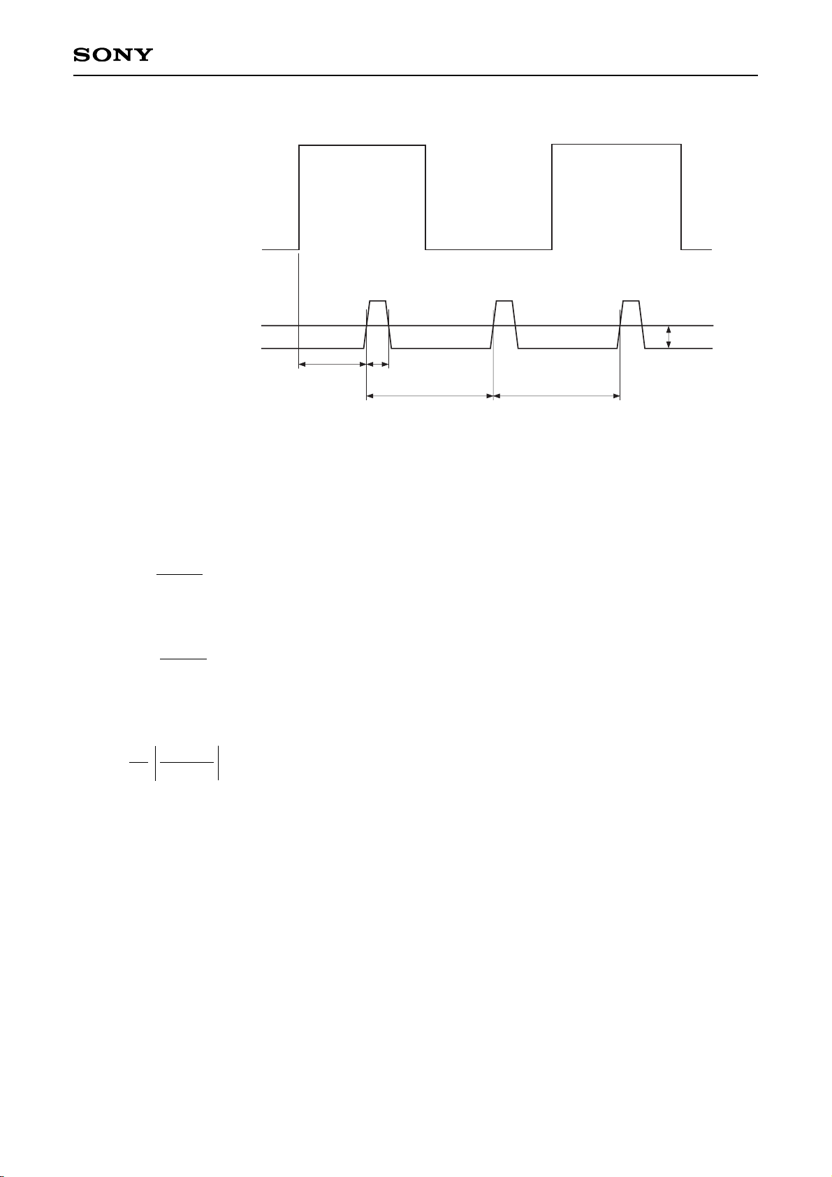
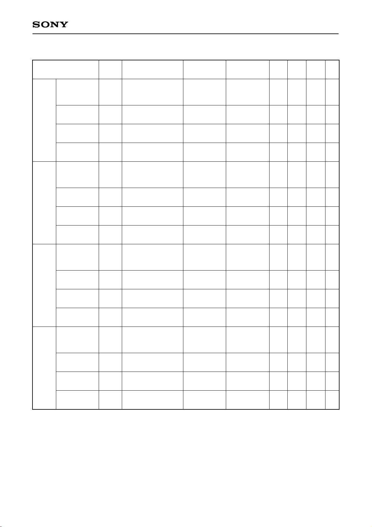
Fig. 1. 1st and 2nd monostable multivibrator pulse width precision
and peak shift measurement conditions
• 1st monostable multivibrator pulse width precision
When X360 = "X" and XHD = "H":
ETM1 = ( –1) × 100 [%]
When X360 = "X" and XHD = "L":
ETM1' = ( –1) × 100 [%]
• 2nd monostable multivibrator pulse width = T2
• Peak shift
PS = × 100 [%]
T1
2.5µs
12TA – TB
TA + TB
T1
1.29µs
External Comparator Output
(Measurement point C)
T1 T2
TA TB
1.4V
Read data output
(Measurement point D)
Page 9
– 9 –
CXA3071N
∗3
Gpn = 20 Log10 (VFilterout/VPreout)
VFilterout = Filter differential output voltage
(N = 1 to 4).
Read System (Filters) (Ta = 25°C, VCC = 5V)
Peak
frequency
Peak voltage
gain
∗3
Frequency
response (1)
Frequency
response (2)
Peak
frequency
Peak voltage
gain
∗3
Frequency
response (1)
Frequency
response (2)
Peak
frequency
Peak voltage
gain
∗3
Frequency
response (1)
Frequency
response (2)
Peak
frequency
Peak voltage
gain
∗3
Frequency
response (1)
Frequency
response (2)
fo1
Gp1
G11
G12
fo2
Gp2
G21
G22
fo3
Gp3
G31
G32
fo4
Gp4
G41
G42
1M
outer
track
1M
inner
track
1.6M/
2M
outer
track
1.6M/
2M
inner
track
WG = "Z", X360 = "X"
XHD = "H"
OTF = "H"
Refer to Fig. 1
at f01
Refer to Fig. 1
at 1/3f01
Refer to Fig. 1
at 3f01
WG = "Z", X360 = "X"
XHD = "H"
OTF = "L"
Refer to Fig. 1
at f02
Refer to Fig. 1
at 1/3f02
Refer to Fig. 1
at 3f02
WG = "Z", X360 = "X"
XHD = "L"
OTF = "H"
Refer to Fig. 1
at f03
Refer to Fig. 1
at 1/3f03
Refer to Fig. 1
at 3f03
WG = "Z", X360 = "X"
XHD = "L"
OTF = "L"
Refer to Fig. 1
at f04
Refer to Fig. 1
at 1/3f04
Refer to Fig. 1
at 3f04
1
1
1
1
1
1
1
1
1
1
1
1
1
1
1
1
A, B
A, B
A, B
A, B
A, B
A, B
A, B
A, B
A, B
A, B
A, B
A, B
A, B
A, B
A, B
A, B
165.6
4.1
–7.4
–24.9
177.2
4.1
–7.4
–24.9
311.3
4.2
–7.4
–25.3
346.2
5.8
–8.3
–37.8
184.0
6.0
–6.9
–23.0
196.9
6.0
–6.9
–23.0
345.9
6.1
–6.9
–23.4
384.6
7.7
–7.8
–35.9
202.4
7.6
–6.4
–21.4
216.6
7.6
–6.4
–21.4
380.5
7.7
–6.4
–21.8
423.0
9.3
–7.3
–34.3
kHz
dB
dB
dB
kHz
dB
dB
dB
kHz
dB
dB
dB
kHz
dB
dB
dB
Item Symbol Conditions
Measurement
circuit
Measurement
point
Min. Typ. Max. Unit
Page 10
– 10 –
CXA3071N
Write/Erase System (Ta = 25°C, VCC = 5V)
Damping resistor
precision
1M/outer track write
current
1M/inner track write
current
1.6M/outer track
write current
1.6M/inner track
write current
2M/outer track write
current
2M/inner track write
current
Write current output
unbalance
Head I/O pin leak
current for writes
Write head pin
current at saturation
Erase current
Erase current output
pin leak current
RD
IWLO
IWLI
IWMO
IWMI
IWHO
IWHI
DW
ILKW
ISW
IE
ILKE
VCC = 0V
SW1 = b
WG = "H", OTF = "H"
XHD = "H", X360 = "X"
WG = "H", OTF = "L"
XHD = "H", X360 = "X"
WG = "H", OTF = "H"
XHD = "L", X360 = "L"
WG = "H", OTF = "L"
XHD = "L", X360 = "L"
WG = "H", OTF = "H"
XHD = "L", X360 = "H"
WG = "H", OTF = "L"
XHD = "L", X360 = "H"
WG = "H"
WG = "H"
WG = "H", OTF = "H"
XHD = "H", X360 = "X"
VSW = 1V, SW2 = b
XEG = "L"
XEG = "L"
2
2
2
2
2
2
2
2
2
2
2
2
A', B'
C', D'
A, B
C, D
A, B
C, D
A, B
C, D
A, B
C, D
A, B
C, D
A, B
C, D
A, B
C, D
A, B
C, D
A, B
C, D
E, F
E, F
–20
8.83
6.62
7.44
5.95
4.18
2.76
–1
—
8.45
5.40
—
—
9.5
7.12
8.0
6.4
4.5
2.97
—
—
9.5
6.0
—
+20
10.17
7.62
8.56
6.85
4.82
3.18
+1
10
10.55
6.60
10
%
mA0-p
mA0-p
mA0-p
mA0-p
mA0-p
mA0-p
%
µA
mA0-p
mA
µA
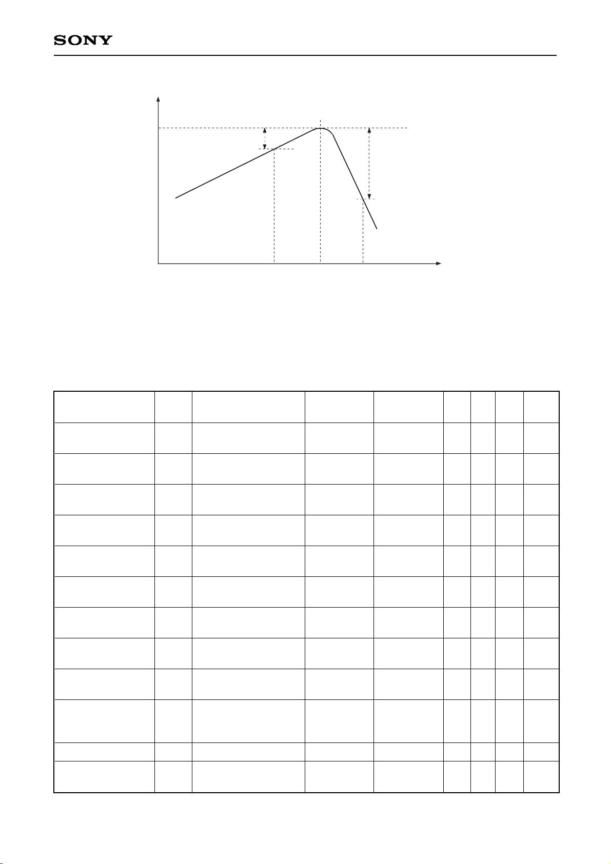
Gn1
Gn2
f [Hz]
3fonfon1/3fon
[dB]
Gpn
(n = 1 to 4)
Fig. 2. Filter frequency response measurement conditions
Item Symbol Conditions
Measurement
circuit
Measurement
point
Min. Typ. Max. Unit
Page 11
– 11 –
CXA3071N
Logic Input Block (Ta = 25°C, VCC = 5V)
Item Symbol Conditions
Measurement
circuit
Measurement
point
Min. Typ. Max. Unit
Digital signal input
low input voltage
Digital signal input
high input voltage
Schmitt-type digital
signal input low input
voltage
Schmitt-type digital
signal input high
input voltage
WG pin digital signal
input high input
voltage
WG pin digital signal
input low input
voltage
Digital signal input
low input current
Digital signal input
high input current
VLD
VHD
VLSD
VHSD
VMHD
VMLD
ILD
IHD
VL = 0V
VH = 5V
2
2
2
2
2
2
2
2
I, J, K, L, M
I, J, K, L, M
G
G
H
H
G, H, I,
J, K, L, M
G, H, I,
J, K, L, M
—
2.0
—
2.0
0.7VCC
—
–100
—
—
—
—
—
—
—
—
—
0.8
—
0.8
—
—
0.3VCC
—
100
V
V
V
V
V
V
µA
µA
Page 12
– 12 –
CXA3071N
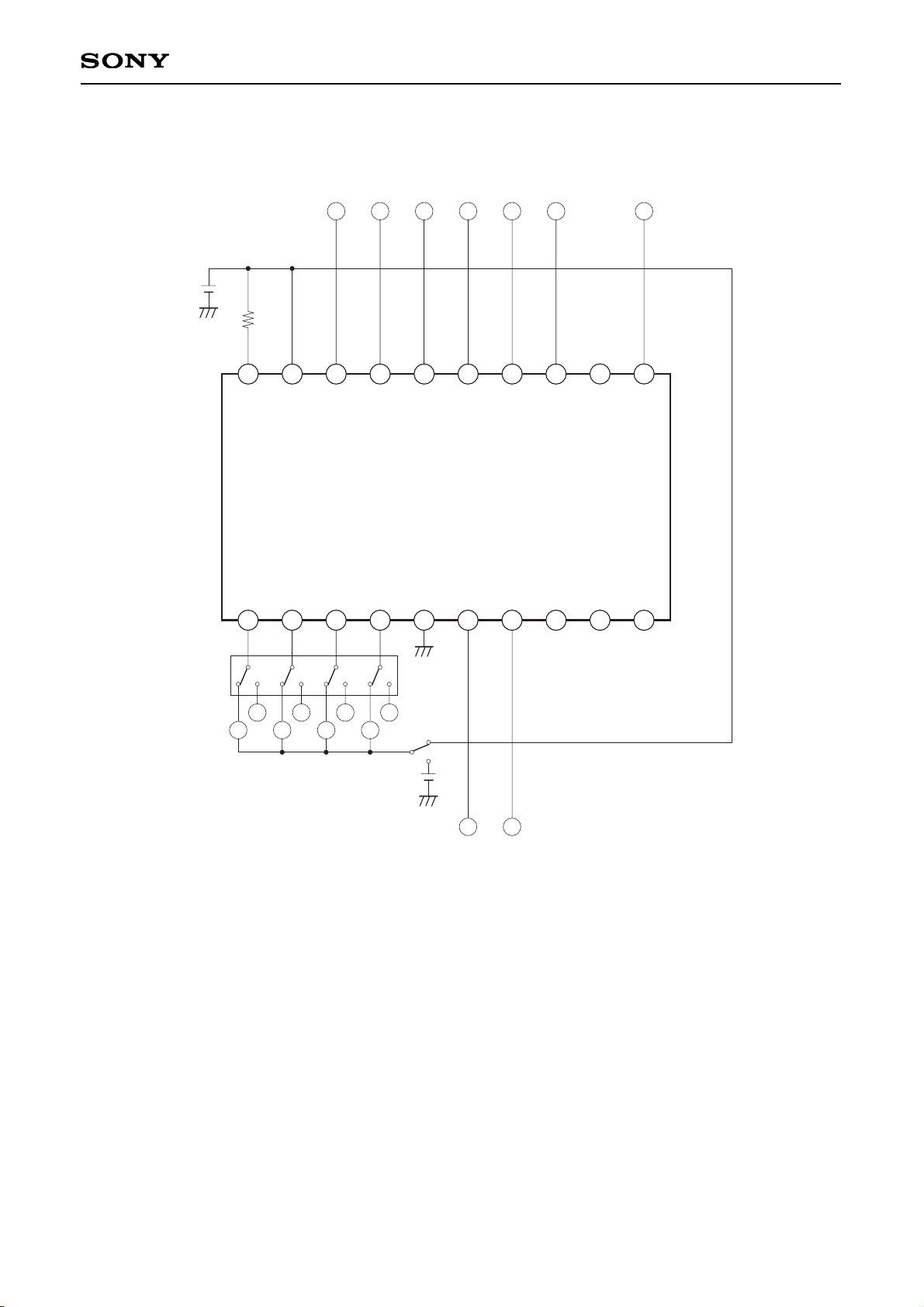
Electrical Characteristics Measurement Circuit 1
C
3300p
3300p
12k
B
A
abab
Vi
1
2
– Vi
1
2
SW1
10kΩ
D
ab
SW5
5V
ab
SW4abSW3abSW2
2
3
4
5
6
7
8
9
10
1
11
12
13
14
15
16
17
18
19
20
HEAD1A
HEAD1B
HEAD0A
HEAD0B
GND
ERA0
ERA1
PONOUT
MONITORA
MONITORB
SETR
V
CC
X360
XHD
OTF
XS1
XEG
WG
RD
XWD
External Comparator
Note) Unless otherwise specified, switches are assumed to be set to "a".
CR time constant of external comparator input stage is equivalent to the time constant of comparator
input stage within the IC.
Page 13
– 13 –
CXA3071N
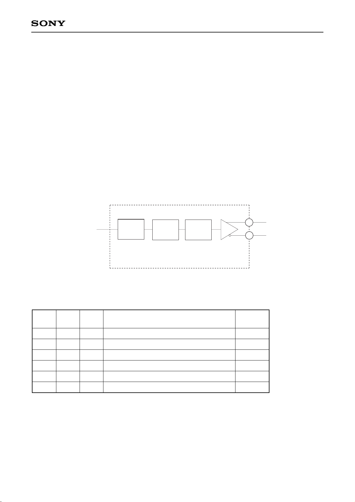
Electrical Characteristics Measurement Circuit 2
FE
a b
SW1
10k
G
5V
H
I
J
K
LM
VSW
a b a b a b
A' B' C' D'
B C D
A
SW2
2
3
4
5
6
7
8
9
10
1
11
12
13
14
15
16
17
18
19
20
HEAD1A
HEAD1B
HEAD0A
HEAD0B
GND
ERA0
ERA1
PONOUT
MONITORA
MONITORB
SETR
V
CC
X360
XHD
OTF
XS1
XEG
WG
RD
XWD
a
b
Note) Unless otherwise specified, switches are assumed to be set to "a".
Page 14
– 14 –
CXA3071N
Description of Operation
(1) Read system
Preamplifier
The preamplifier amplifies input signals.
The voltage gain can be switched depending on the settings of Pins 16, 17 and 18.
Filter
The filter differentiates the signals amplified by the preamplifier. The high-band noise components are
attenuated by the low-pass filter.
The filters can be switched among four modes, depending on the settings of Pins 16, 17 and 18.
In 1M/outer track mode, the peak frequency f01 is fixed and used as a reference (1.00), and f0 for the other
three modes is switched by the internal settings of the IC.
Active filter block
BPF
LPF HPF
Preamplifier output
MONITORA
MONITORB
Secondary
f
OB = 1.2 × fC
Q = 0.577
Tertiary
fc: variable
Primary
fCH = 5kHz
Gain: 8dB
Amp
9
10
Filter block
The center frequency f0B of the BPF is fixed to 1.2 times the cutoff frequency f0 of the LPF. The LPF
characteristics are set to Chebyshev (1dB ripple) for 1.6M, 2M/inner track mode only, and the Butterworth for
all other modes.
Pin16
OTF
Pin17
XHD
Pin18
X360
LPF characteristics
f0 ratio
H
L
H
L
H
L
H
H
L
L
L
L
X
X
L
L
H
H
1M/outer track: Butterworth
1M/inner track: Butterworth
1.6M/outer track: Butterworth
1.6M/inner track: Chebyshev 1dB ripple
2M/outer track: Butterworth
2M/inner track: Chebyshev 1dB ripple
1.00
1.07
1.88
2.09
1.88
2.09
Page 15
– 15 –
CXA3071N
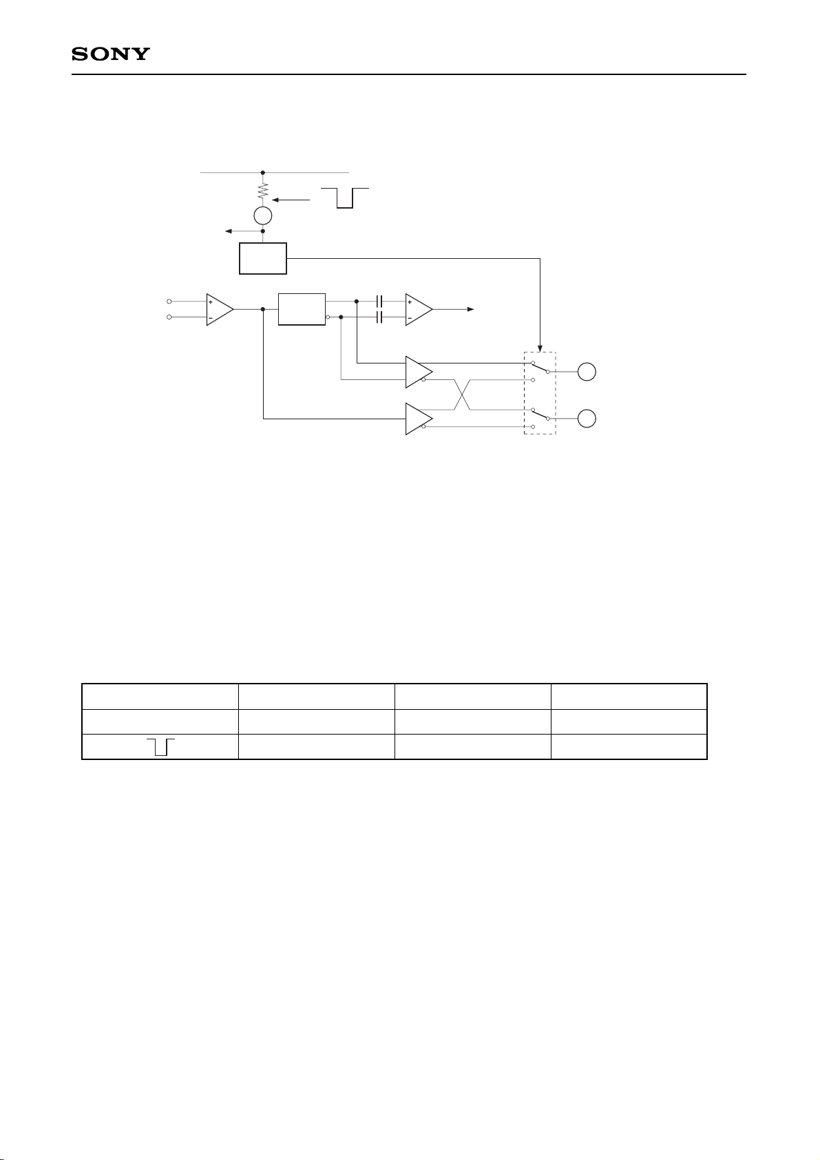
Monitor switching
20
LATCH
FILTER
COMP
TDF
PREAMP
9
10
FILA
MONITORA
PREA
FILB
PREB
MONITORB
SW switching signal
"L" pulse
SETR
REF AMP
refR
V
CC
SW
The monitor pins are used for both the preamplifier output and filter output. These pins are set to filter output
during normal read mode, but the preamplifier output can be monitored by temporarily setting the SETR pin
(Pin 20) to Low.
The monitored contents are returned from the preamplifier output to the filter output by switching to write
mode (WG = Z → High).
Note that the specifications for inputting a low signal to the SETR pin are the same as for the TTL input pin,
but an open collector output (or open drain output) should be used while inputting the signal.
SETR (Pin 20)
Z
MONITORA (Pin 9)
FILOUTA
PREOUTA
MONITORB (Pin 10)
FILOUTB
PREOUTB
Monitor mode
Filter output
Preamplifier output
Monitor block configuration
Page 16

– 16 –
CXA3071N
Comparator
The comparator detects the crosspoint of the filter differential output.
Time domain filter
The time domain filter converts the comparator output to read data.
This filter is equipped with two monostable multivibrators. 1st monostable multivibrator eliminates unnecessary
pulses, and 2nd monostable multivibrator determines the pulse width of the read data.
Note that the 1st monostable multivibrator pulse width T1 is fixed internally.
T1 can be switched as follows by the settings of Pins 17 and 18:
When XHD = "H" and X360 = "X": T1 (1M) = 2500 [ns]
When XHD = "L" and X360 = "L" or
XHD = "L" and X360 = "H": T1(1.6M/2M) = 1290 [ns]
The pulse width for 2nd monostable multivibrator is fixed at 400 [ns].
(2) Write system
Write data input through Pin 11 is frequency-divided by the T flip-flop and generates the recording current for
the head. The recording current can be switched by the settings of Pins 17 and 18. Note that the write current
IW is fixed internally for each mode.
Furthermore, the inner/outer track write current IW can be changed for each mode by switching Pin 16.
However, the current ratio between the inner and outer tracks is fixed.
(3) Erase current
The erase current IE is fixed internally.
Pins 6 and 7 are constant current outputs.
(4) Power ON/OFF detection system
The power ON/OFF detection system detects a reduced voltage in the supply voltage.
When VCC is below the specified value, the write system and erase system cease operation, disabling the
write and erase functions.
Notes on Operation
• Select the voltage gain so that the preamplifier output amplitude is 1Vp-p or less.
If the preamplifier output amplitude exceeds 1Vp-p, the filter output waveform becomes distorted.
• Observe the following point when mounting this device.
• The GND should be as large as possible.
• Connect a VCC decoupling capacitor of about 0.1µF as close to the device as possible.
Page 17
– 17 –
CXA3071N
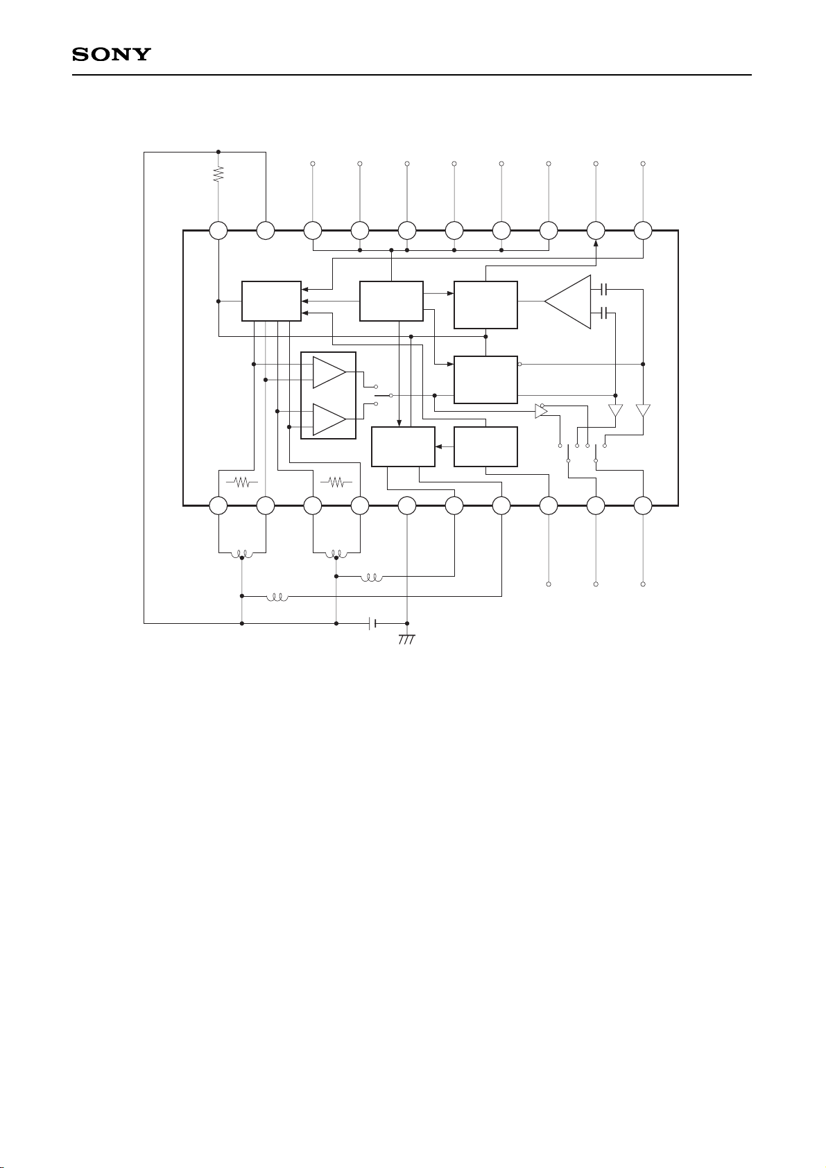
Application Circuit
HEAD1A
HEAD1B
HEAD0A
HEAD0B
GND
ERA0
ERA1
PONOUT
MONITORA
MONITORB
SETR
V
CC
X360
XHD
OTF
XS1
XEG
WG
RD
XWD
WRITE
DRIVER
PREAMP
CONTROL
LOGIC
TIME
DOMAIN
FILTER
FILTER
DIFF + LPF
(BPF)
POWER
MONITOR
ERASE
DRIVER
2
3
4
5
6
7
8
9
10
1
11
12
13
14
15
16
17
18
19
20
10kΩ
VCC
COMP
Note) When using two modes (1M and 2M), connect X360 (Pin 18) to VCC and set XHD (Pin 17) high or low to
switch modes.
Application circuits shown are typical examples illustrating the operation of the devices. Sony cannot assume responsibility for
any problems arising out of the use of these circuits or for any infringement of third party patent and other right due to same.
Page 18

– 18 –
CXA3071N
Filter Frequency Response
The LPF characteristics are set to Chebyshev (1dB ripple) for 1.6M, 2M/inner track mode only, and to
Butterworth for other modes. The 1.6M and 2M characteristics and fc ratio are identical.
fon
(Differential characteristics)
f
OB
B.P.F
Q = 0.577
fcn
(Comprehensive characteristics)
(High-band noise cutoff)
L.P.F
Tertiary Butterworth
L.P.F
Tertiary Chebyshev
1dBRp
(n = 1, 2, 3)
fc4
fo4
1M/outer track, inner track
1.6M, 2M/outer track
1.6M, 2M/inner track
The BPF center frequency f0B is fixed at 1.2 times the LPF cutoff frequency.
f0B = 1.2fc
In the comprehensive characteristics, the relationship between the peak frequencies f0 and fc is as follows,
depending on the differences of the LPF type:
Butterworth characteristics fcn = 1.28f0n (n = 1, 2, 3)
Chebyshev (1dB ripple characteristics) fC4 = 1.09f04
Page 19

– 19 –
CXA3071N
Custom Selection of Filters
The LPF cutoff frequency fc in 1M/outer track mode can be customized. In addition, assuming the LPF cutoff
frequency value as 1.00, the fc ratio can be selected for the other three modes.
In addition, the LPF characteristics are set to Chebyshev (1dB ripple) for 1.6M, 2M/inner track mode only, and
to Butterworth for the other modes. However, a custom selection can be made between Chebyshev (1dB
ripple) and Butterworth for 1.6M, 2M/inner track mode only. (However, the 1.6M and 2M characteristics and fc
ratio are identical.)
Note that the BPF center frequency f0B is fixed at 1.2 times fc.
1.0
1.07 , 1.14, 1.23, 1.33, 1.45, 1.60, 2.00
1.23, 1.33, 1.39, 1.45, 1.52, 1.60, 1.68,
1.78, 1.88 , 2.00, 2.13, 2.29, 2.46, 2.67
1.23, 1.33, 1.39, 1.45, 1.52, 1.60, 1.68,
1.78 , 1.88, 2.00, 2.13, 2.29, 2.46, 2.67
Butterworth
Butterworth
Butterworth
Butterworth
Chebyshev (1dB ripple)
1M/outer track
1M/inner track
1.6M, 2M/outer track
1.6M, 2M/inner track
Mode LPF type
fc ratio when fC1 is assumed as 1
∗
The boxed ratio indicates the setting for the CXA3071N.
Write Current Setting Method
Assuming the outer track as 1.00, the write current ratio is fixed within the IC for each mode.
The write current for the outer track is fixed within the IC.
The setting is for the outer track current when OTF is High, and for the inner track current when OTF is Low.
1.00, 0.92, 0.86, 0.80, 0.75 , 0.71, 0.66, 0.63
1.00, 0.92, 0.86, 0.80 , 0.75, 0.71, 0.66, 0.63
1.00, 0.92, 0.86, 0.80 , 0.75, 0.71, 0.66 , 0.63
1M mode
1.6M mode
2M mode
Track
Write current inner track setting ratio
∗
The boxed ratio indicates the setting for the CXA3071N.
Page 20
– 20 –
CXA3071N
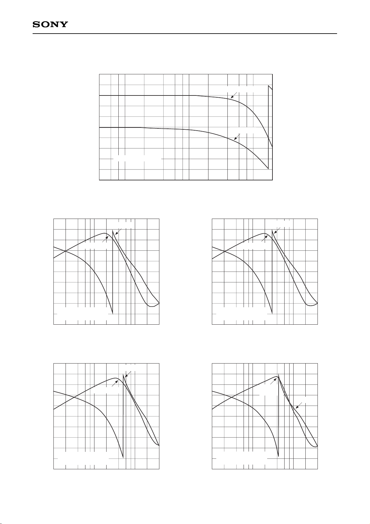
Normalized preamplifier voltage gain and phase vs. Frequency
f — Frequency [Hz]
100k 10M1M
Normalized preamplifier voltage gain [dB]
0
–16
–12
–8
–4
Phase [deg]
–180
–90
0
90
180
VCC = 5V, Ta = 25°C
Voltage gain
Phase
Frequency [Hz]
1M/outer track
10k 4M1M
Normalized filter voltage gain [dB]
–80
40k 100k 400k
f
01 = 184.0 [kHz]
Phase [deg]
180
90
0
–90
–180
VCC = 5V, Ta = 25°C
R = 10kΩ
Voltage gain
Phase
0
–60
–40
–20
20
1M/inner track
10k 4M1M
Normalized filter voltage gain [dB]
0
–80
–60
–40
–20
40k 100k 400k
Phase [deg]
180
90
0
–90
–180
Frequency [Hz]
VCC = 5V, Ta = 25°C
R = 10kΩ
Voltage gain
Phase
f02 = 196.9 [kHz]
20
1.6M, 2M/outer track
10k 4M1M
Normalized filter voltage gain [dB]
0
–80
–60
–40
–20
40k 100k 400k
Phase [deg]
180
90
0
–90
–180
Frequency [Hz]
f
03 = 345.9 [kHz]
VCC = 5V, Ta = 25°C
R = 10kΩ
Voltage gain
Phase
20
1.6M, 2M/inner track
10k 4M1M
Normalized filter voltage gain [dB]
0
–80
–60
–40
–20
40k 100k 400k
Phase [deg]
180
90
0
–90
–180
Frequency [Hz]
f
04 = 384.6 [kHz]
VCC = 5V, Ta = 25°C
R = 10kΩ
Voltage
gain
Phase
20
Example of Representative Characteristics
Page 21
– 21 –
CXA3071N
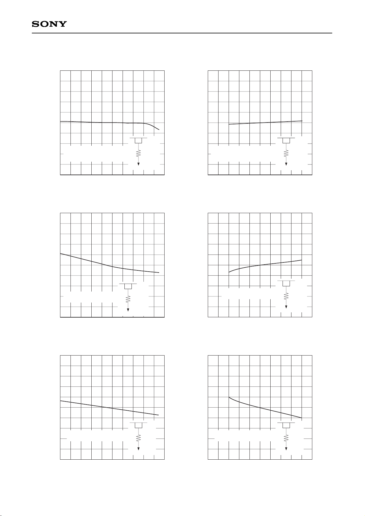
Normalized preamplifier voltage gain +
filter voltage gain NGv vs. Ambient temperature Ta
Ta — Ambient temperature [°C]
0.50
1.00
1.50
NGv — Normalized preamplifier voltage gain + filter voltage gain
VCC = 5V
f = 100kHz
NGV = GV/GV (Ta = 25°C)
VCC
10kΩ
20
Normalized preamplifier voltage gain +
filter voltage gain NGv vs. Supply voltage Vcc
Vcc — Supply voltage [V]
–20 0 20 40 60 80
4.0 5.0 6.0
0.50
1.00
1.50
NGv — Normalized preamplifier voltage gain + filter voltage gain
Ta = 25°C
f = 100kHz
NGV = GV/GV (VCC = 5V)
VCC
10kΩ
20
–20
Normalized filter peak frequency NfO vs.
Ambient temperature Ta
Ta — Ambient temperature [°C]
0 20 40 60 80
0.95
1.00
1.05
Nf
O
— Normalized filter peak frequency
VCC = 5V
Nf0 = f0/f0 (Ta = 25°C)
VCC
10kΩ
20
Vcc — Supply voltage [V]
4.0 5.0 6.0
0.95
1.00
1.05
VCC
10kΩ
20
Nf
O
— Normalized filter peak frequency
Ta = 25°C
Nf0 = f0/f0 (VCC = 5V)
Ta — Ambient temperature [°C]
0.95
1.00
1.05
NT
1
— Normalized 1st monostable multivibrator pulse width
VCC = 5V
NTA = T1/T1 (Ta = 25°C)
10kΩ
20
0 20 40 60 80–20
VCC
Vcc — Supply voltage [V]
4.0 5.0 6.0
0.95
1.00
1.05
NT
1
— Normalized 1st monostable multivibrator pulse width
Ta = 25°C
NTA = T1/T1 (VCC = 5V)
10kΩ
20
VCC
Normalized filter peak frequency NfO vs.
Supply voltage Vcc
Normalized 1st monostable multivibrator pulse
width NT
1 vs. Ambient temperature Ta
Normalized 1st monostable multivibrator pulse
width NT1 vs. Supply voltage Vcc
Page 22
– 22 –
CXA3071N
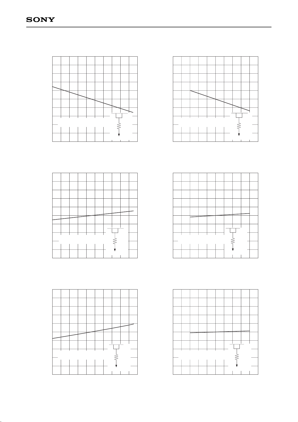
Normalized read data pulse width NT2 vs.
Ambient temperature Ta
Ta — Ambient temperature [°C]
0.95
1.00
1.05
NT
2
— Normalized read data pulse width
VCC = 5V
NTB = T2/T2 (Ta = 25°C)
0 20 40 60 80–20
Vcc — Supply voltage [V]
4.0 5.0 6.0
0.95
1.00
1.05
NT
2
— Normalized read data pulse width
Ta = 25°C
NTB = T2/T2 (VCC = 5V)
Ta — Ambient temperature [°C]
0.95
1.00
1.05
NIw — Normalized write current
VCC = 5V
NIW = IW/IW (Ta = 25°C)
VCC
10kΩ
20
0 20 40 60 80–20
Vcc — Supply voltage [V]
4.0 5.0 6.0
0.95
1.00
1.05
NIw — Normalized write current
Ta = 25°C
NIW = IW/IW (VCC = 5V)
VCC
10kΩ
20
Vcc — Supply voltage [V]
4.0 5.0 6.0
0.95
1.00
1.05
NI
E
— Normalized erase current
Ta = 25°C
NIE = IE/IE (VCC = 5V)
10kΩ
20
VCC
Ta — Ambient temperature [°C]
0.95
1.00
1.05
VCC = 5V
NIE = IE/IE (Ta = 25°C)
NI
E
— Normalized erase current
10kΩ
20
VCC
0 20 40 60 80–20
VCC
10kΩ
20
VCC
10kΩ
20
Normalized read data pulse width NT2 vs.
Supply voltage Vcc
Normalized write current NIw vs.
Supply voltage Vcc
Normalized write current NIw vs.
Ambient temperature Ta
Normalized erase current NI
E vs.
Ambient temperature Ta
Normalized erase current NIE vs.
Supply voltage Vcc
Page 23
– 23 –
CXA3071N
Ta — Ambient temperature [°C]
–20
0 20 40 60 80
3.6
4.1
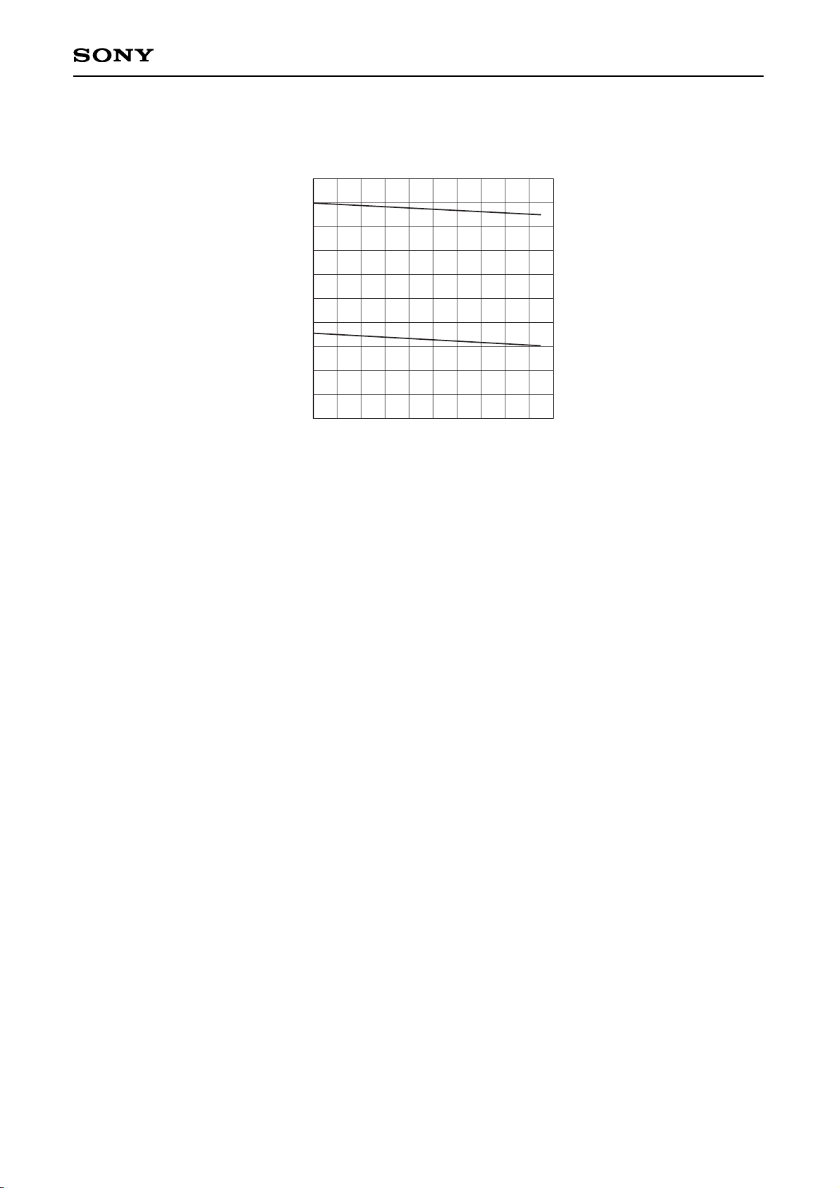
Power supply ON/OFF detector threshold
voltage VTH vs. Ambient temperature Ta
V
TH
— Power supply ON/OFF detector threshold voltage [V]
3.8
4.0
3.7
3.9
Page 24
– 24 –
CXA3071N
Package Outline Unit: mm
20PIN SSOP (PLASTIC)
SONY CODE
EIAJ CODE
JEDEC CODE
PACKAGE STRUCTURE
PACKAGE MATERIAL
LEAD TREATMENT
LEAD MATERIAL
PACKAGE WEIGHT
EPOXY RESIN
SOLDER / PALLADIUM
COPPER / 42 ALLOY
0.1g
SSOP-20P-L01
SSOP020-P-0044
0.1 ± 0.1
0.5 ± 0.2
0° to 10°
DETAIL A
PLATING
∗6.5 ± 0.1
∗4.4 ± 0.1
0.22 – 0.05
+ 0.1
0.65 ± 0.12
20
11
10
1
A
0.1
+ 0.05
1.25 – 0.1
+ 0.2
0.15 – 0.02
6.4 ± 0.2
NOTE: Dimension “∗” does not include mold protrusion.
NOTE : PALLADIUM PLATING
This product uses S-PdPPF (Sony Spec.-Palladium Pre-Plated Lead Frame).
 Loading...