

Page 1
—1—
E96932A8Z
Sony reserves the right to change products and specifications without prior notice. This information does not convey any license by
any implication or otherwise under any patents or other right. Application circuits shown, if any, are typical examples illustrating the
operation of the devices. Sony cannot assume responsibility for any problems arising out of the use of these circuits.
Absolute Maximum Ratings (Ta = 25 °C)
• Supply voltage VCC 14 V
• Operating temperature range
Topr –35 to +80 °C
• Storage temperature range
Tstg –65 to +150 °C
Operating Conditions
Supply voltage VCC 2.7 to 3.3 V
Description
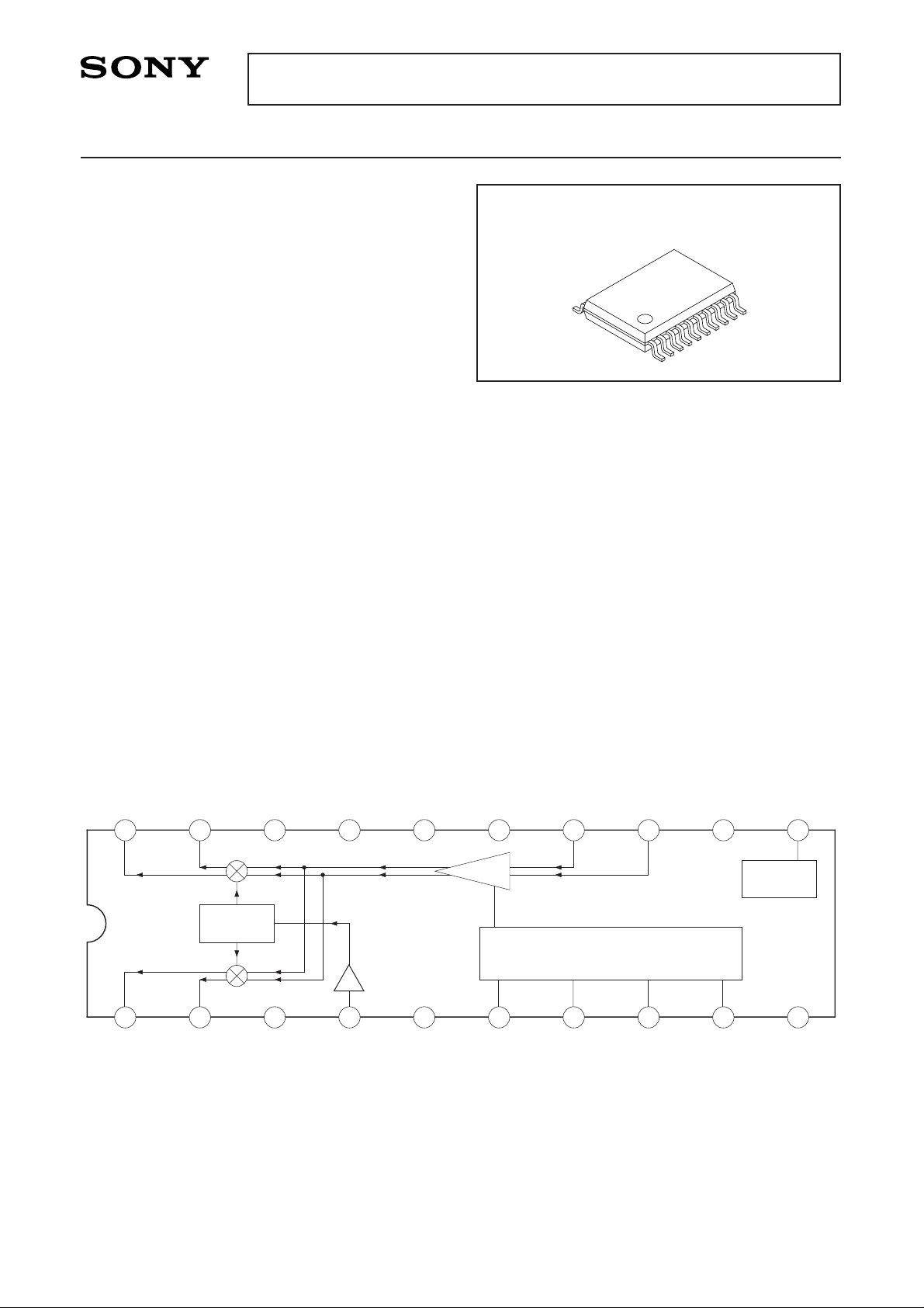
The CXA3174N is a 4-bit digital control variable
gain amplifier suitable for the communications.
Features
• Gain control amplifier with the wide gain variable
range
• Doubler circuit for the LO (local) signal eliminates
need for the phase shifter
Functions
• IF signal gain control circuit
• I/Q quadrature demodulator
• Doubler circuit for the LO signal
• Gain control by the 4-bit digital data
• Power saving
Applications
GSM and PCS portable telephones
Structure
Bipolar silicon monolithic IC
AGC IF for GSM/PCS
20 pin SSOP (Plastic)
CXA3174N
Block Diagram and Package Outline
Reg
QXOUT
QOUT
LOIN
NC
VC4
VC3
VC2
VC1
NC
NC
IXOUT
IOUT
NC
NC
GND
V
CC
IFIN
IFINX
NC
PS
× 2
Gain Control AMP
1 3 4 5 6 7 8 9 102
11121314151617181920
Gain Cont
Phase
Shifter
For the availability of this product, please contact the sales office.
Page 2
—2—
CXA3174N
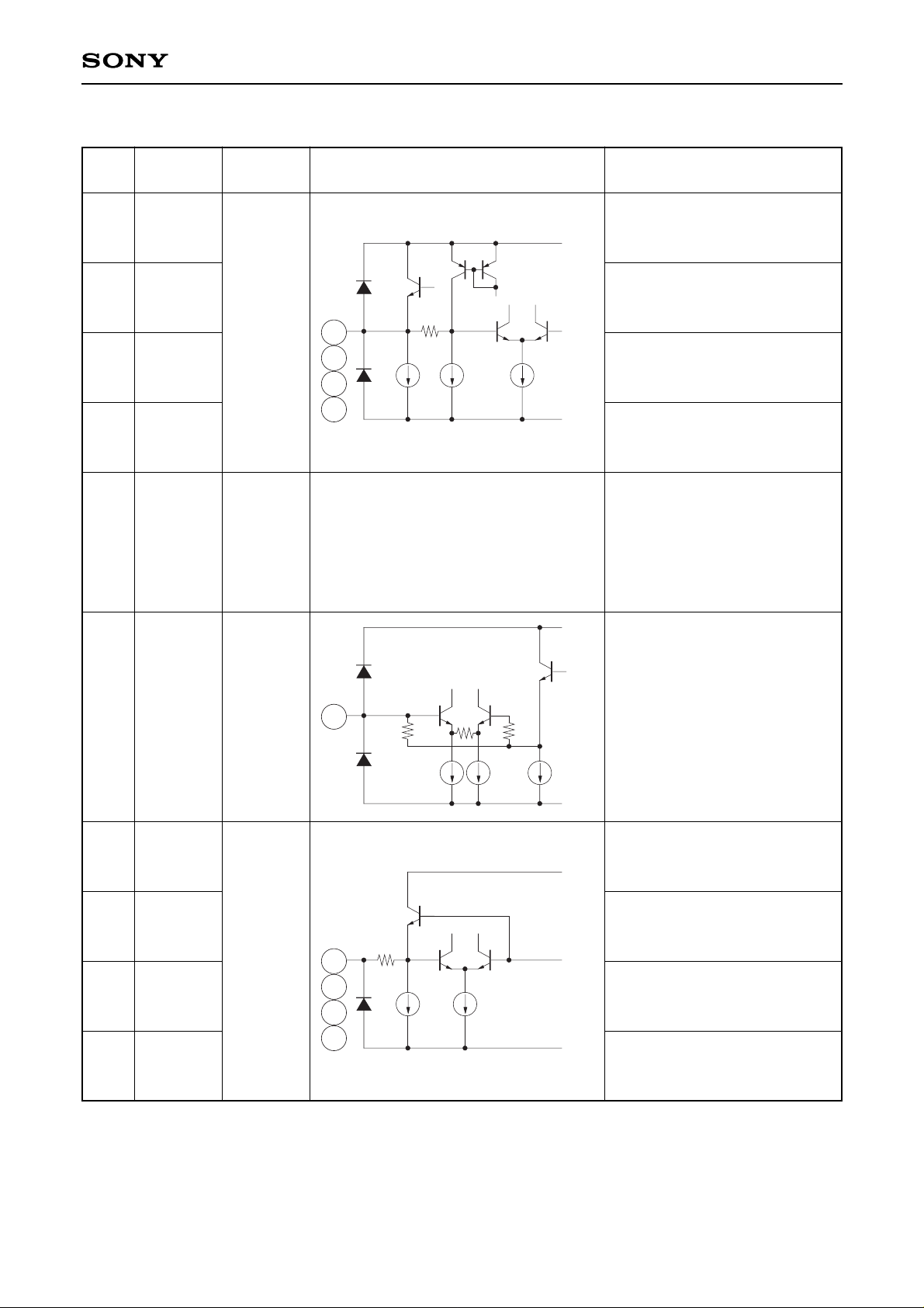
Pin Description
Pin
Symbol Pin voltage Equivalent circuit Description
No.
1
2
19
20
3
5
10
12
17
18
4
6
7
8
9
QXOUT
QOUT
IOUT
IXOUT
NC
LOIN
VC4
VC3
VC2
VC1
1.5 V
—
1.3 V
—
Q inverted signal output.
Q signal output.
I signal output.
I inverted signal output.
Not connected.
Local signal input.
AGC control signal input. MSB.
AGC control signal input. 3LSB.
AGC control signal input. 2LSB.
AGC control signal input. LSB.
1
2
20
19
VCC
GND
5.4k
VCC
GND
6
7
8
9
40k
VCC
GND
4
2k 2k
500
Page 3
—3—
CXA3174N
Pin
Symbol Pin voltage Equivalent circuit Description
No.
11
13
14
15
16
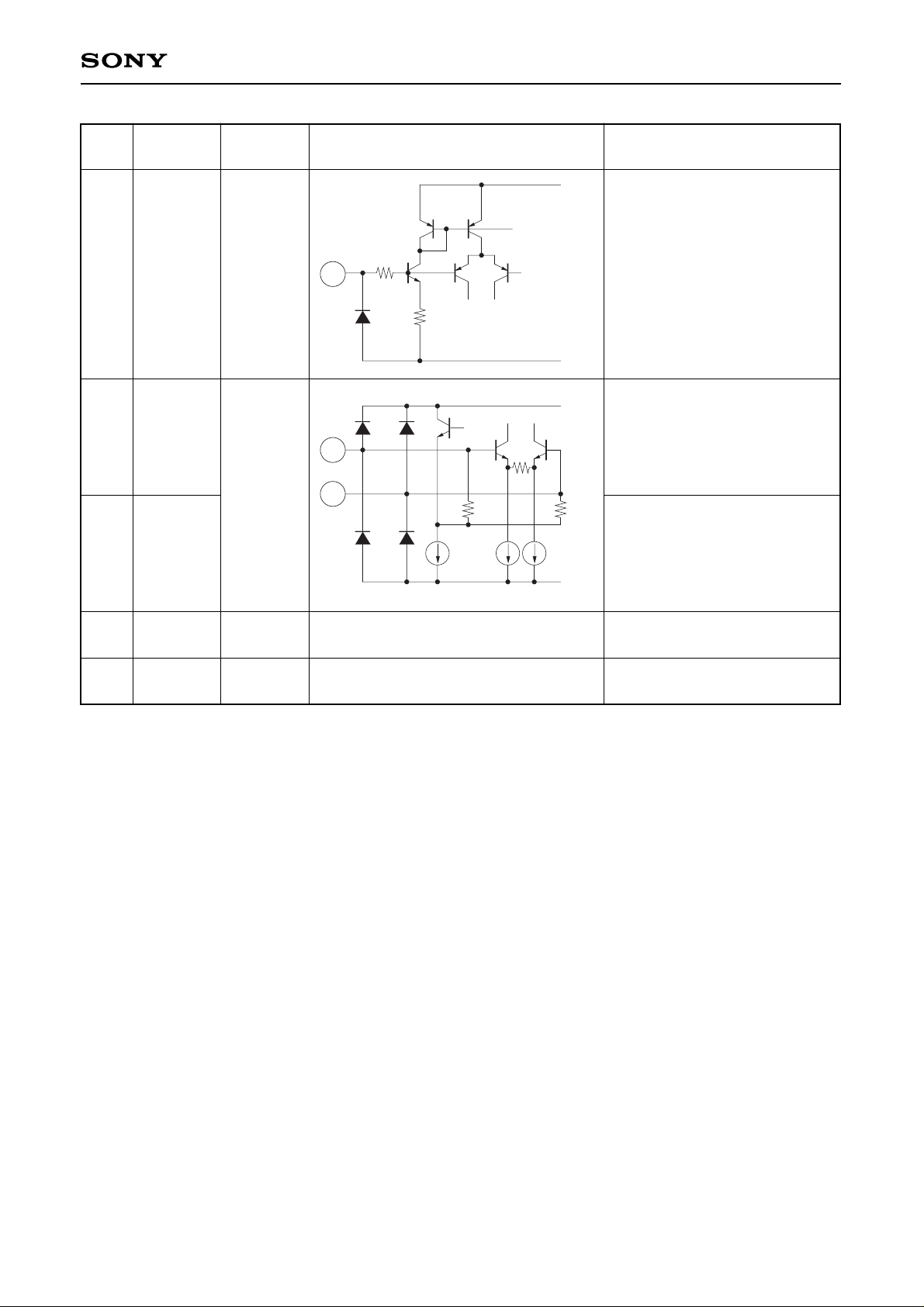
PS
IFINX
IFIN
VCC
GND
—
1.25 V
—
—
Power saving control.
IF inverted signal input.
IF signal input.
Power supply.
Ground.
VCC
GND
11
40k
60k
VCC
GND
13
14
1.1k 1.1k
800
Page 4

—4—
CXA3174N
Electrical Characteristics VCC = 3.0 V, Ta = 27 °C
Item Symbol Conditions Min. Typ. Max. Unit
Current consumption
Current consumption
for standby
IF input
frequency range
Maximum gain
Minimum gain
Gain variable step
Gain setting deviation
Gain setting time
LO input
frequency range
LO input level
I/Q output
frequency range
I/Q output
signal amplitude
I/Q output
maximum amplitude1
I/Q output
maximum amplitude2
I/Q output
maximum amplitude3
I/Q output
maximum amplitude4
I/Q output
amplitude deviation
ICC
ICCps
IFINf
Gmax
Gmin
Gstep
Gdev
Gt
LOINf
LOINv
IQf
IQv
IQvmax1
IQvmax2
IQvmax3
IQvmax4
IQvdev
PS=0 V
VC1, 2, 3, 4 = all “Low”
∗1, ∗2
Temperature fluctuation : ±2 dB
IF input level : –80 dBm
(330 Ω conversion)
VC1, 2, 3, 4 = all “High”
∗1, ∗2
Temperature fluctuation : ±2 dB
IF input level : –20 dBm
(330 Ω conversion)
Differential I/Q output amplitude
∗1, ∗2
10 kΩ load IF input level : –20 dBm
(330 Ω conversion) Gain=0 dB
Differential I/Q output amplitude
10 kΩ load Gain=60 dB
∗2
Differential I/Q output amplitude
10 kΩ load Gain=40 dB
∗2
Differential I/Q output amplitude
10 kΩ load Gain=20 dB
∗2
Differential I/Q output amplitude
10 kΩ load Gain=0 dB
∗2
Differential I/Q output amplitude
∗1, ∗2
10 kΩ load IF input level : –20 dBm
(330 Ω conversion) Gain=0 dB
10 15 mA
10 100 µA
5 20 MHz
57 60 63 dB
–3 0 –3 dB
4 dB
–3 +3 dB
5 µS
5 20 MHz
30 55 80 mVrms
2000 kHz
45 64 91 mVp-p
2.0 2.7 Vp-p
2.0 2.4 Vp-p
400 480 mVp-p
210 250 mVp-p
–0.5 0.5 dB
∗1
The IF input level is the value of C4 in the Application Circuit.
∗2
The measured value is for the differential output.
Page 5
—5—
CXA3174N
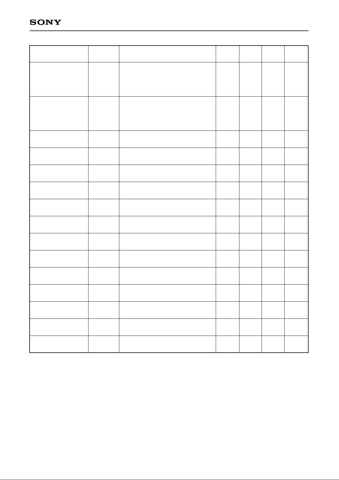
Item Symbol Conditions Min. Typ. Max. Unit
I/Q output
phase deviation1
I/Q output
phase deviation2
I/Q output DC voltage
I/Q output
DC voltage deviation
Noise figure1
Noise figure2
Tertiary intercept
point1
Tertiary intercept
point2
PS input ON voltage
Logic input
High voltage
Logic input
Low voltage
Logic input
resistance
LOIN input resistance
IFIN input resistance
IFIN input level
IQpdev1
IQpdev2
IQvdc
IQvdcd
NF 1
NF 2
IP31
IP32
VpsL
VCvH
VCvL
VCr
LOINr
IFINr
IFINv
Differential I/Q output
∗1, ∗2
10 kΩ load IF input level : –20 dBm
(330 Ω conversion) Gain=0 dB
LO input level : 30 mVrms
Differential I/Q output
∗1, ∗2
10 kΩ load IF input level : –20 dBm
(330 Ω conversion) Gain=0 dB
LO input level : 80 mVrms
I-IX, Q-QX
Output voltage difference
Gain=60 dB
Gain=20 dB
Gain=60 dB, 330 Ω conversion
∗1
Gain=20 dB, 330 Ω conversion
∗1
Differential input
330 Ω conversion
–2.5 2.5 deg
–2.5 2.5 deg
1.4 1.5 1.6 V
–30 30 mV
22.5 dB
40 dB
–49 dBm
–30 dBm
0 0.8 V
2.2 VCC+0.3 V
0 0.8 V
30 kΩ
1.4 2 2.6 kΩ
1.5 2.2 2.9 kΩ
–90 –10 dBm
Page 6
—6—
CXA3174N
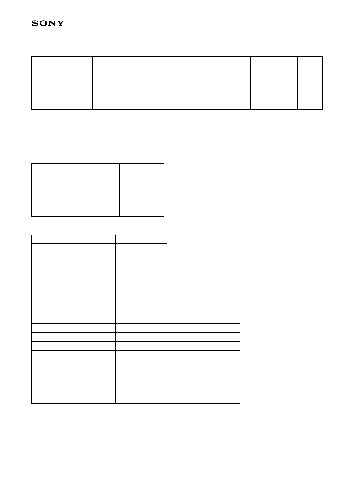
Control 1 Power saving
Control 2 Gain setting
Pin 11 (PS)
H
L
Power saving
off
on
IC status
Active
Sleep
Pin No. 6 7 8 9
Symbol VC4 VC3 VC2 VC1 4-bit Setting gain
MSB 3LSB 2LSB LSB display (dB)
MAX
MIN
“0000”
“0001”
“0010”
“0011”
“0100”
“0101”
“0110”
“0111”
“1000”
“1001”
“1010”
“1011”
“1100”
“1101”
“1110”
“1111”
60
56
52
48
44
40
36
32
28
24
20
16
12
8
4
0
L L L L
L L L H
L L H L
L L H H
L H L L
L H L H
L H H L
L H H H
H L L L
H L L H
H L H L
H L H H
H H L L
H H L H
H H H L
H H H H
Note on Operation
Take care to handle the IC because the electrostatic discharge strength is weak for Pins 6, 7, 8, 9 and 11.
Item Symbol Conditions Min. Typ. Max. Unit
LOIN input
capacitance
IFIN input
capacitance
LOINc
IFINc Differential input
2 pF
1.2 pF
Design Reference
∗1
The IF input level is the value of C4 in the Application Circuit.
∗2
The measured value is for the differential output.
Page 7
—7—
CXA3174N
60
50
40
30
20
10
0
Gain (dB)
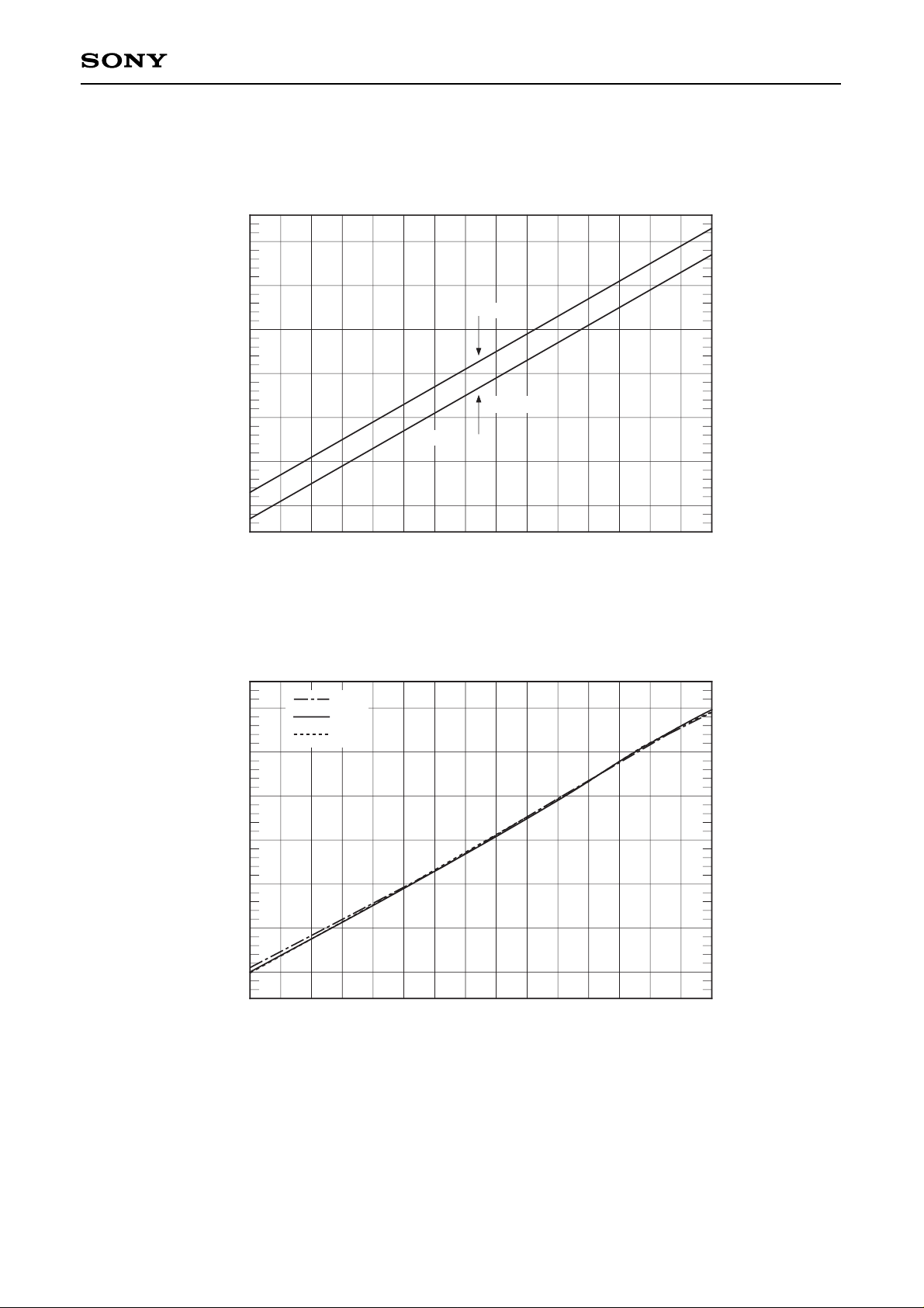
Gain control characteristics
V
CC=3.0V, Ta=27°C
1111 1010 0101 0000
Gain setting value (4bits)
Upper
Lower
60
50
40
30
20
10
0
Gain (dB)
Example of gain control temperature characteristics
V
CC=3.0V
1111 1010 0101 0000
Gain setting value (4bits)
- 35°C
Rt
80°C
6dB width
Page 8
—8—
CXA3174N
Reg
P9
P8
P7
P6
GNDGNDGND
QXOUT
QOUT
LOIN
NC
VC4
VC3
VC2
VC1
NC
NC
P1
C1
QXOUT
GND
10k
R1
S1
1µ
C1
QXOUT
P2
C2
QOUT
GND
10k
R3
S2
1µ
C3
QOUT
C3
LOIN
P4
LOIN
S3
1µ
C5
GND
R5
50
VC4
VC3
VC2
VC1
GND
10k
R2
1µ
C2
P20
IXOUT
C6
IXOUT
S8
10k
R4
C4
1µ
P19
IOUT
C5
IOUT
S7
GND
GND GND GND
P15
V
CC
C6
10µ
C7
1000p
S6
P14
IFIN
C9
1000p
C10
1000p
C4
IF
R7
280
GND
GND
C8
0.01µ
R6
390
S4
P13
IFINX
GND
P11
PS
IXOUT
IOUT
NC
NC
GND
V
CC
IFIN
IFINX
NC
PS
× 2
Gain Control AMP
11121314151617181920
1 3 4 5 6 7 8 9 102
S5
Gain Cont
Phase
Shifter
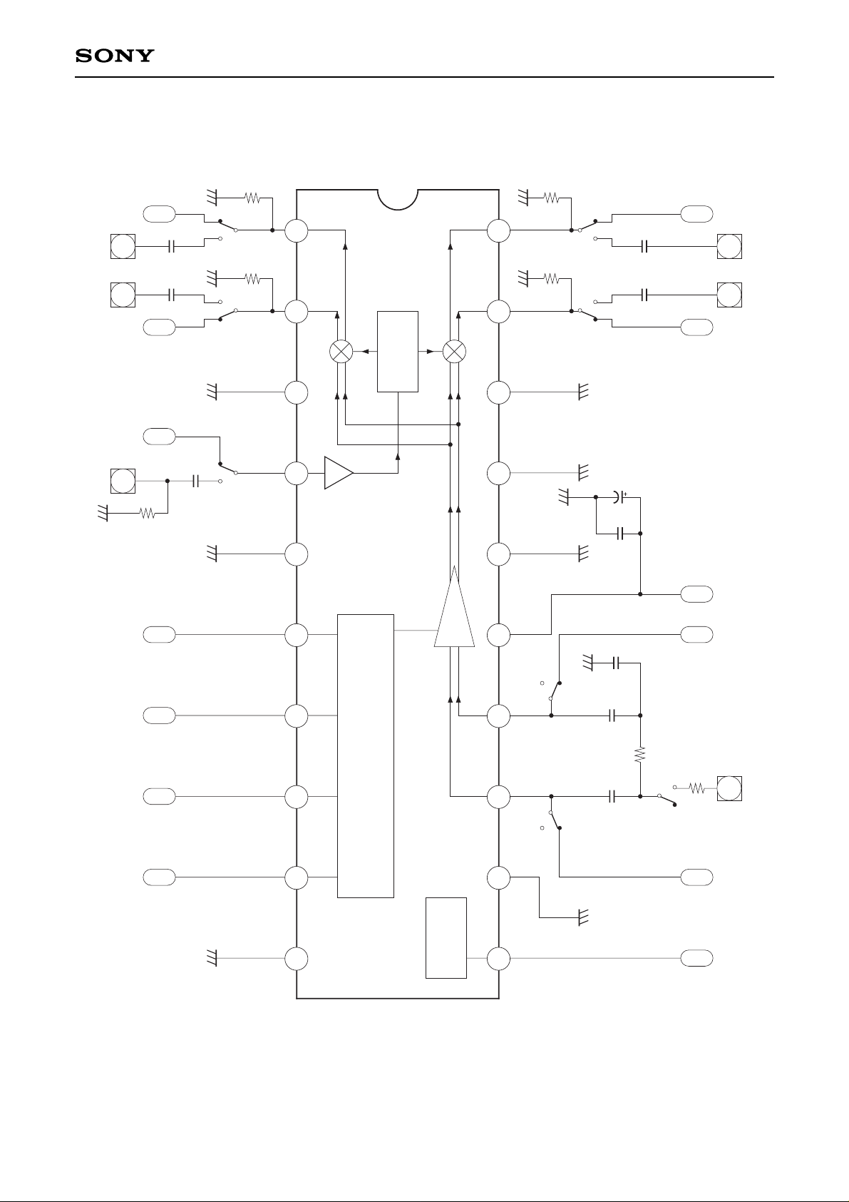
Electrical Characteristics Measurement Circuit
Page 9
—9—
CXA3174N
Reg
P9
P8
P7
P6
GNDGNDGND
QXOUT
QOUT
LOIN
NC
VC4
VC3
VC2
VC1
NC
NC
C1
1µ
QXOUT
C2
GND
10k
1µ
QOUT
C3
LOIN
1µ
VC4
VC3
VC2
VC1
GND
10k
1µ
C6
IXOUT
10k
1µ
C5
IOUT
GND
GND GND GND
P15
V
CC
10µ
1000p
1000p
1000p
C4
IF
GND
GND
0.01µ
390
P11
PS
IXOUT
IOUT
NC
NC
GND
V
CC
IFIN
IFINX
NC
PS
× 2
Gain Control AMP
1 3 4 5 6 7 8 9 102
GND
10k
GND
11121314151617181920
SAW
5p
5.6µ 6.8p to 45p
GND
Gain Cont
Phase
Shifter
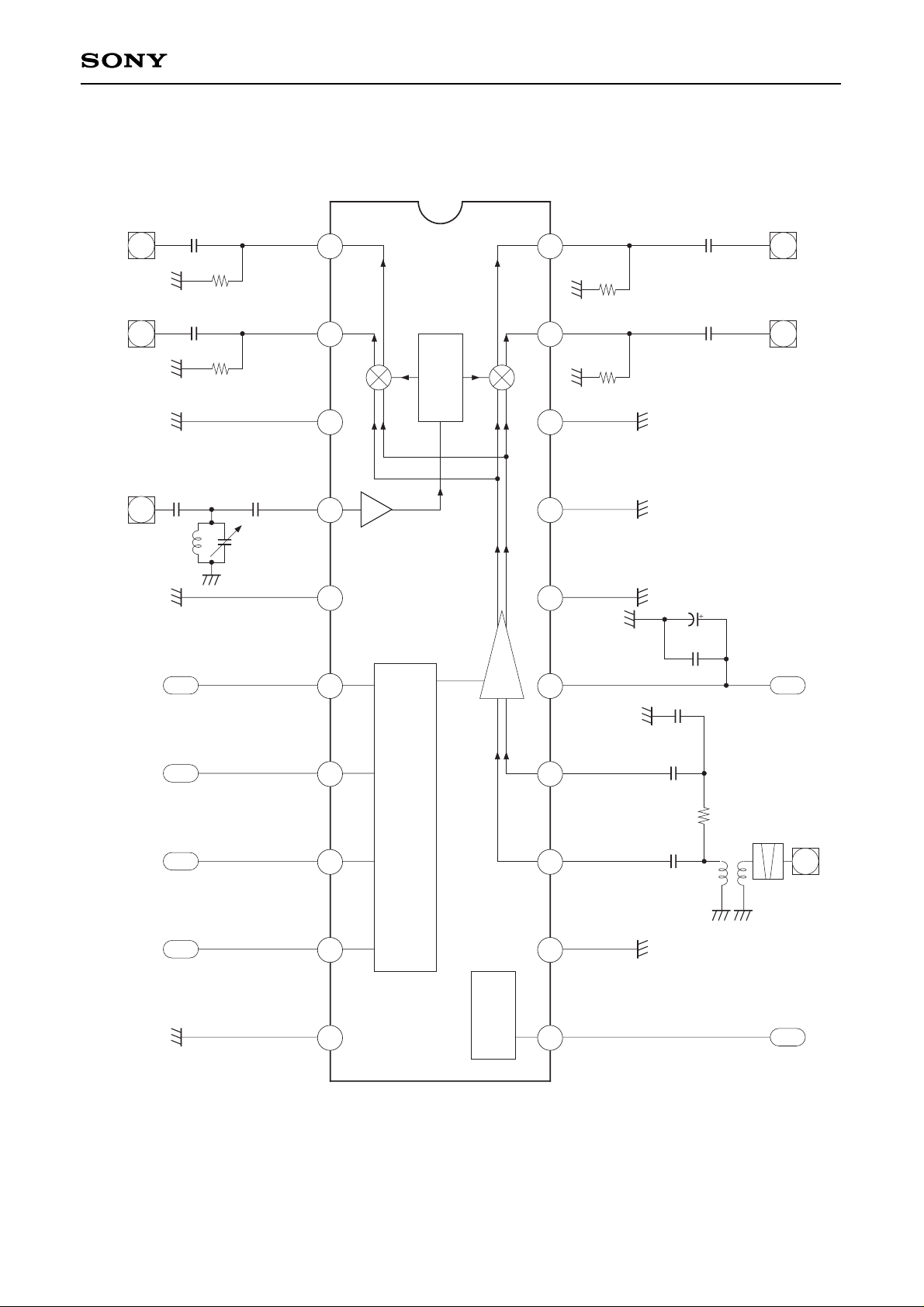
Application Circuit
Application circuits shown are typical examples illustrating the operation of the devices. Sony cannot assume responsibility for
any problems arising out of the use of these circuits or for any infringement of third party patent and other right due to same.
Page 10
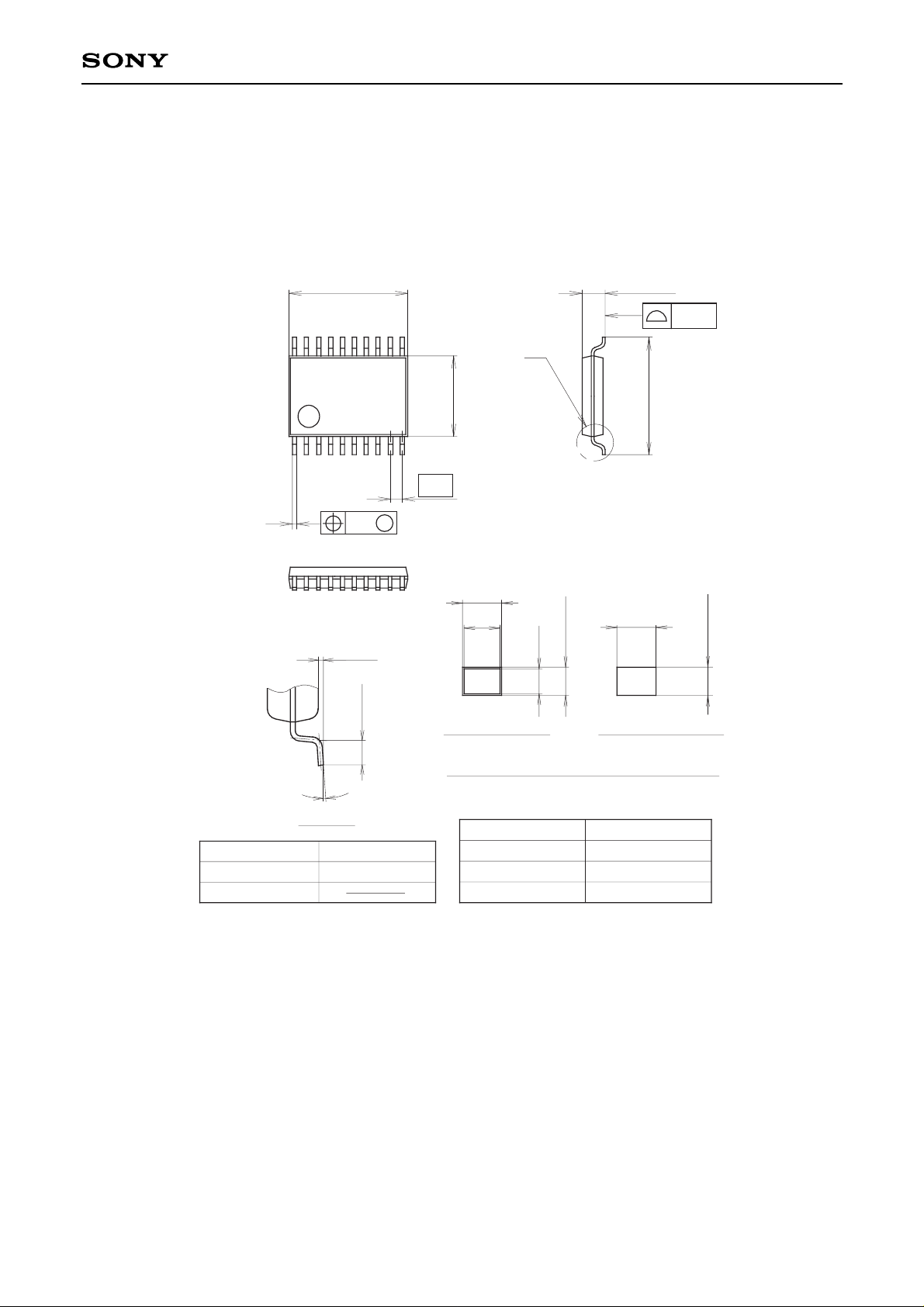
20PIN SSOP (PLASTIC)
SONY CODE
EIAJ CODE
JEDEC CODE
PACKAGE STRUCTURE
PACKAGE MATERIAL
LEAD TREATMENT
LEAD MATERIAL
PACKAGE MASS
EPOXY RESIN
SOLDER / PALLADIUM
42/COPPER ALLOY
0.1g
SSOP-20P-L01
SSOP020-P-0044
PLATING
0.1 ± 0.1
0.5 ± 0.2
0° to 10°
DETAIL A
NOTE: Dimension “∗” does not include mold protrusion.
b=0.22 – 0.05
+ 0.1
0.15 – 0.02
+ 0.05
(0.22)
(0.15)
0.15 – 0.01
DETAIL B : SOLDER DETAIL B : PALLADIUM
+ 0.03
b=0.22 ± 0.03
∗6.5 ± 0.1
∗4.4 ± 0.1
0.65
20
11
10
1
A
0.1
1.25 – 0.1
+ 0.2
6.4 ± 0.2
0.13
M
b
Package Outline Unit : mm
CXA3174N
—10—
NOTE : PALLADIUM PLATING
This product uses S-PdPPF (Sony Spec.-Palladium Pre-Plated Lead Frame).
 Loading...