

Page 1

—1—
E98822A8Y
Sony reserves the right to change products and specifications without prior notice. This information does not convey any license by
any implication or otherwise under any patents or other right. Application circuits shown, if any, are typical examples illustrating the
operation of the devices. Sony cannot assume responsibility for any problems arising out of the use of these circuits.
Description
CXA3202AN is a TX gain control amplifier suitable
for CDMA cellular/PCS phone.
Features
• Wide gain control range
• Linear gain slope
• Wideband operation (50 MHz to 300 MHz)
• Very small package (16 Pin SSOP)
• Low voltage operation
• High output IP3
• Power save function included
Absolute Maximum Ratings
• Supply voltag VCC 6V
•Operating temperature Topr –55 to +125 °C
• Storage temperature Tstg –65 to +150 °C
• Allowable Power dissipation PD 330 mW
• Supply voltage range –0.3 to 6 V
• Logic input voltage –0.3 to VCC + 0.3 V
• Signal input voltage –0.3 to VCC + 0.3 V
•
Differential signal input voltage
0 to 2.5 V
Operating Condition
Supply voltage VCC 2.7 to 3.8 V
Applications
CDMA cellular/PCS phone
Structure
Bipolar silicon monolithic IC
TX Gain Control Amplifier
16 pin SSOP (Plastic)
CXA3202AN
Page 2
—2—
CXA3202AN
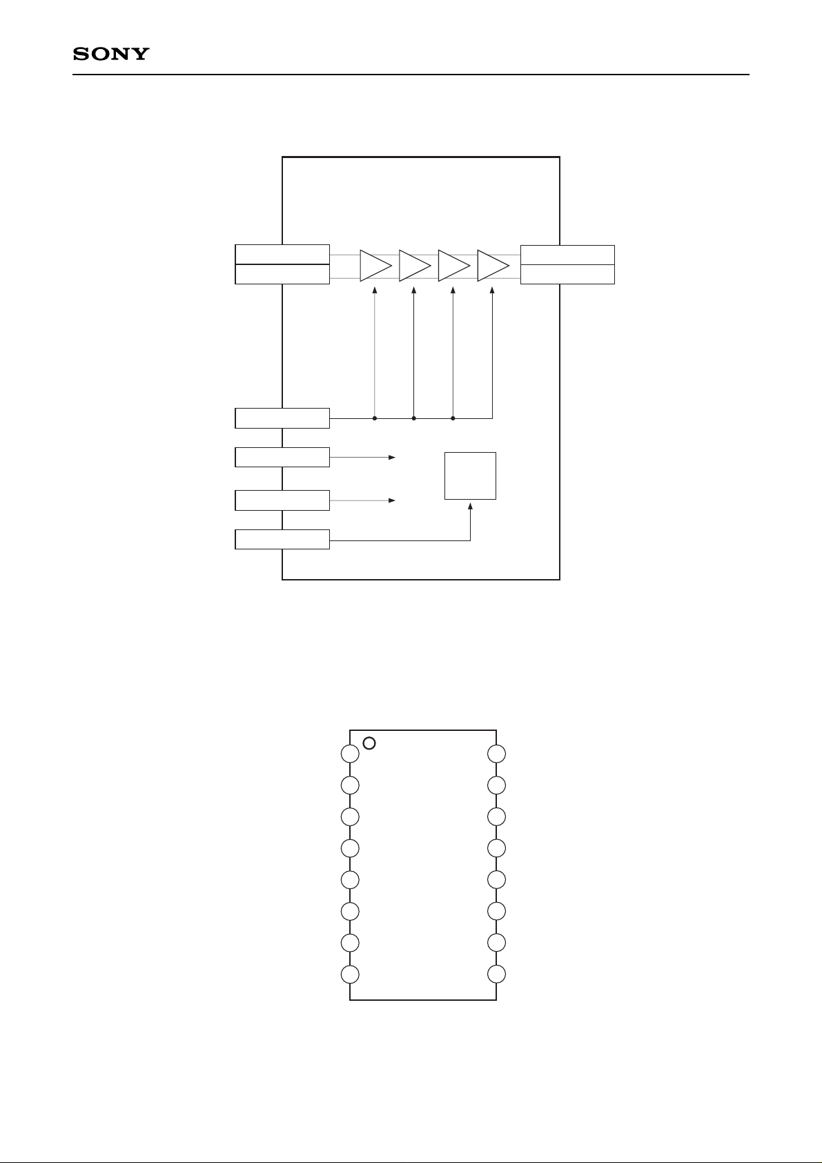
Block Diagram
Pin Configuration
OUT
OUTX
GCTL
VCC1, 2
GND1, 2
PSV
CDMA IN
CDMA INX
Bias
Driver
IF Input
Gain control
Supply Voltage
Ground
Power Save
IF Output
16
15
14
13
12
11
10
9
1
2
3
4
5
6
7
8
CDMA IN
CDMA INX
NC
GND1
GND2
NC
NC
PSV
GCTL
NC
V
CC1
V
CC2
GND1
GND2
OUT
OUTX
Page 3
—3—
CXA3202AN
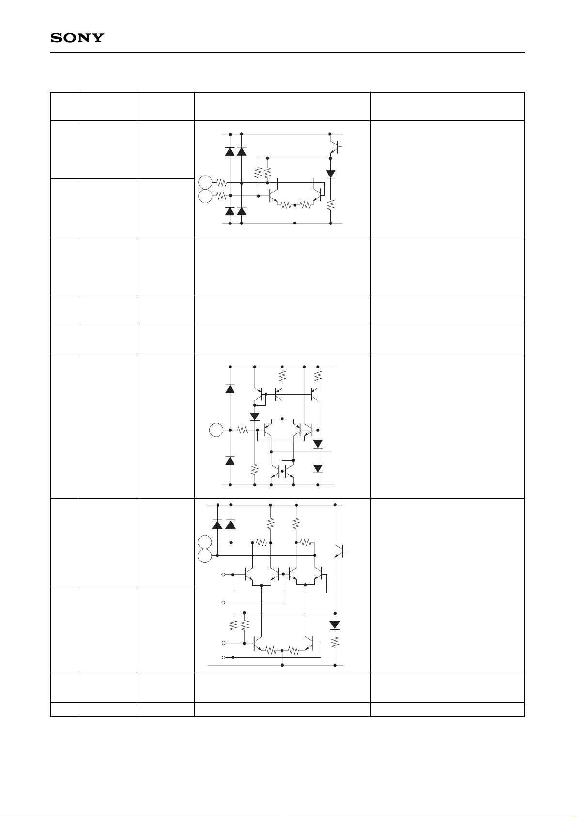
Pin Description
Pin
Symbol
Pin voltage
Equivalent circuit Description
No. TYP (V)
1
2
3
6
7
15
4
12
5
11
8
9
10
13
14
CDMA IN
CDMA INX
NC
GND1
GND2
PSV
OUTX
OUT
VCC2
VCC1
1.1
1.1
0
0
—
—
—
3.0
3.0
40k
200
200
40k
VCC1
GND1
1
2
135k
8
VCC1
GND
12.25k
510
510
12.25k
9
10
V
CC2
GND2
Differential input pins for CDMA
transmit IF signal.
No connection.
Ground
Ground
Power save function pin.
High: Active
Low: Power save
Differential output pins for transmit
IF signal.
Open collector output.
Positive power supply for output
stage.
Positive power supply.
Page 4
—4—
CXA3202AN
Pin
Symbol
Pin voltage
Equivalent circuit Description
No. TYP (V)
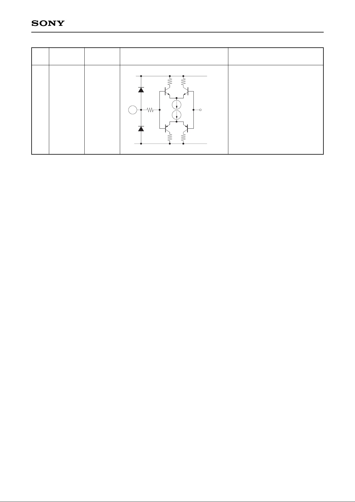
16 GCTL —
6k6k
8k8k
200
16
V
CC1
GND
Gain control pin.
Page 5

—5—
CXA3202AN
Electrical Characteristics
DC Characteristics (VCC=3.0 V, Ta=27 °C)
Parameter
Current consumption 1
Current consumption 2
Input current pin 8H
Input current pin 8L
Input current pin 16H
Input current pin 16L
PSV high voltage
PSV low voltage
Symbol
ICC1
ICC2
IpsvH
IpsvL
IgctlH
IgctlL
VpsH
VpsL
Conditions
Vpsv=3.0 V, Vgctl=1.5 V, Pin 13, 14
Vpsv=0 V, Vgctl=1.5 V, Pin 13, 14
Vpsv=3.0 V
Vpsv=0 V
Vgctl=3.0 V
Vgctl=0.5 V
Pin 8
Pin 8
Min. Typ. Max. Unit
10 15.7 21.5 mA
5 18 40
1
–15 µA
1
–1
2.5
V
0.5
Parameter
Operating frequency
range
Gain 2.3
Gain 1.5
Gain 1.0
Gain 0.7
CDMA Gain slope
Input level 3rd order
intercept point
Noise Figure
Symbol
Fr
G2.3
G1.5
G1.0
G0.7
GCLIN
IIP3
NF
Conditions
f=130.38 MHz, level=–22.5 dBm,
Vgctl=2.3 V
Vgctl=1.5 V
Vgctl=1.0 V
Vgctl= 0.7 V
Gain at Vgctl=2.0 V – Gain at Vgctl=1.0 V
G=15 dB
∗1
f1=129.38 MHz, f2=131.38 MHz
Measure of 130.38 MHz
G=15 dB
∗1
Measure of 130.38 MHz
Min. Typ. Max. Unit
50 300 MHz
13 17 21
–28 –24 –20 dB
–58 –54 –50
–75 –70 –65
57 60 63 dB/V
–8.5 –4.5 dBm
28 32 dB
AC Characteristics (VCC=3.0 V, Ta=27 °C)
∗1
Adjust GCTL voltage, and set the overall gain to 15 dB.
Page 6

—6—
CXA3202AN
Measurement Circuit
2k
1000p
1000p
∗1
A8
V8
10k
A16
0.01µ
V16
A14
0.01µ
V14
2.4k
∗1
OUTPUT
9
10
11
12
13
14
15
16
2
3
4
5
6
7
8
1
GCTL
NC
V
CC1
V
CC2
GND1
GND2
OUT
OUTX
CDMA IN
CDMA INX
NC
GND1
GND2
NC
NC
PSV
CDMA
INPUT
1µ
∗
2
820n
∗
3
820n
∗
3
∗
1
TOKO, Inc. B5FL 616DS-1135
∗
2
Coilcraft, Inc. 1008HS-102TKBC
∗
3
Coilcraft, Inc. 1008HS-821TKBC
Page 7

—7—
CXA3202AN
Application Circuit
∗
1k
0.01µ
0.01µ
1000p
1000p
∗
∗
9
10
11
12
13
14
15
16
2
3
4
5
6
7
8
1
GCTL
NC
VCC1
VCC2
GND1
GND2
OUT
OUTX
CDMA IN
CDMA INX
NC
GND1
GND2
NC
NC
PSV
VCC
∗
Active
Sleep
100p
1000p
1000p
Gain Control
Voltage
TX IF
OUTPUT
TX IF
INPUT
Application circuits shown are typical examples illustrating the operation of the devices. Sony cannot assume responsibility for
any problems arising out of the use of these circuits or for any infringement of third party patent and other right due to same.
∗
Must be adjusting values to result a best impedance matching between BPF filter and this IC.
Page 8

—8—
CXA3202AN
Design Reference Values
Single ended measurement (VCC=3.0 V, Ta=27 °C)
Item
Input resistance
Input capacitance
Output resistance
Output capacitance
Symbol
Rin
Cin
Rout
Cout
Conditions
f=130.38 MHz, Vgctl=1.5 V
Typ. Unit
10 kΩ
0.98 pF
6.0 kΩ
0.92 pF
Notes on Operation
1) This IC is a wideband amplifier with wide gain control range. The decouping capacitors between GND Pin
and VCC Pin should be as close to the IC as possible.
2) The resistors connected to Pins 9 and 10 should be as close to the IC as possible.
3) This IC assumes the excellent characteristics when the differential input impedance between Pins 1 and 2
is 500 Ω. Refer to the Measurement Circuit for the external element settings, etc.
4) Pay attention to handling this IC because its electrostatic discharge strength is weak.
Page 9
—9—
CXA3202AN
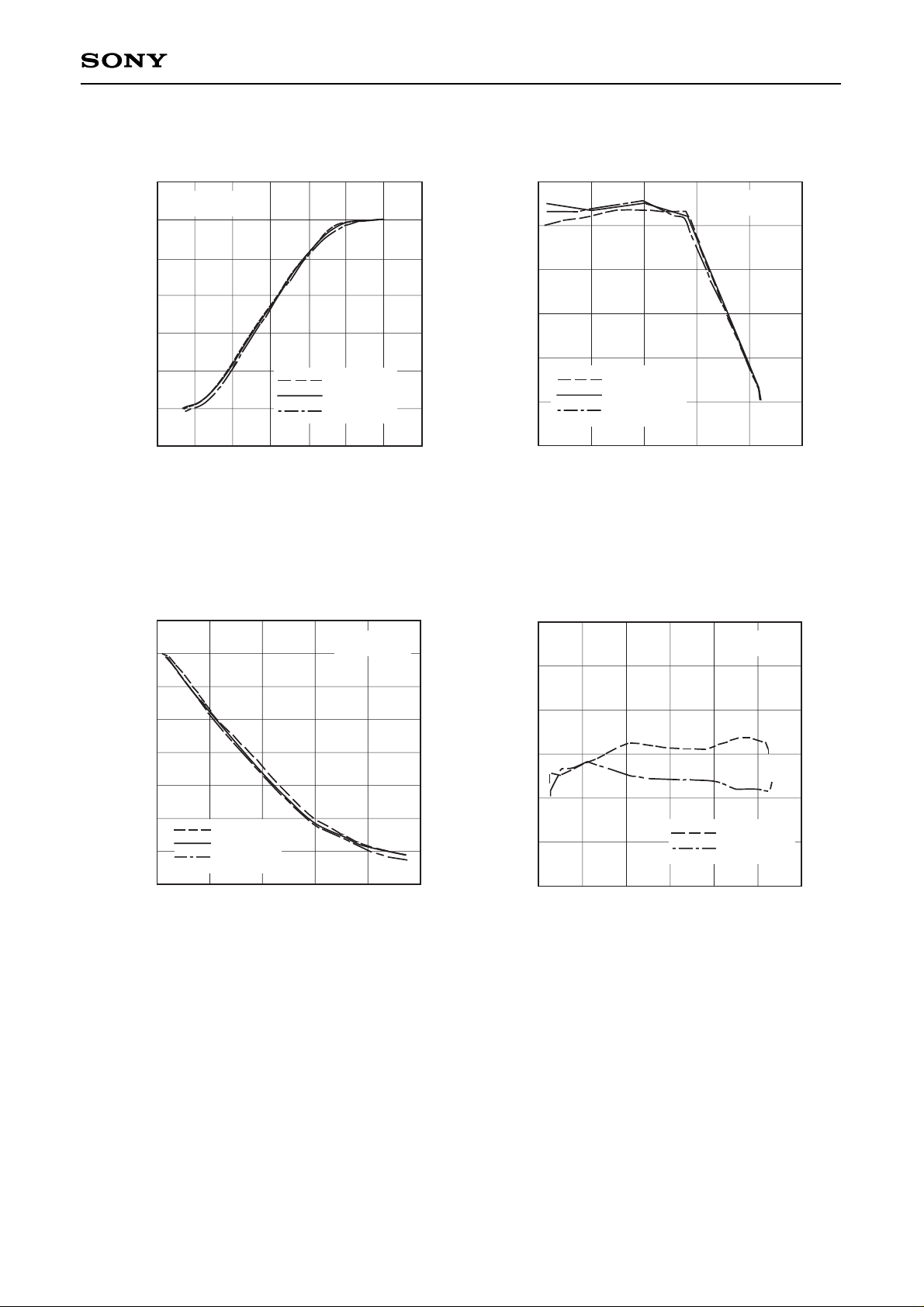
Sensitivity
0
Vgctl [V]
0.5 1 1.5 2 2.5 3
–100
–60
–40
–20
0
20
40
Power gain [dB]
T = –40°C
T = 27°C
T = 85°C
VCC = 3.0V
Noise Figure
–80
Power gain [dB]
–60 –20 0 20
20
30
40
50
60
70
Noise figure [dB]
–40
Gain Error from Room Temp
–80
Power gain [dB]
0 20 40
–6
–4
–2
2
4
6
Gain error [dB]
T = –40°C
T = 85°C
VCC = 3.0V
0
–60 –40 –20
IIP3
Power gain [dB]
–60 –20 0 20 40
–15
–10
–5
0
5
10
15
IIP3 [dBm]
T = –40°C
T = 27°C
T = 85°C
VCC = 3.0V
–40
80
90
VCC = 3.0V
–80
3.5
VCC = 3.0V
T = –40°C
T = 27°C
T = 85°C
100
Page 10

16PIN SSOP (PLASTIC)
SONY CODE
EIAJ CODE
JEDEC CODE
PACKAGE STRUCTURE
PACKAGE MATERIAL
LEAD TREATMENT
LEAD MATERIAL
PACKAGE MASS
EPOXY RESIN
SOLDER / PALLADIUM
42/COPPER ALLOY
0.1g
SSOP-16P-L01
SSOP016-P-0044
∗5.0 ± 0.1
0.65
0.22 – 0.05
+ 0.1
8
1
9
16
∗4.4 ± 0.1
6.4 ± 0.2
0.1 ± 0.1
0.5 ± 0.2
0° to 10°
0.15 – 0.02
+ 0.05
1.25 – 0.1
+ 0.2
A
DETAIL A
0.1
PLATING
NOTE: Dimension “∗” does not include mold protrusion.
0.13
M
Package Outline Unit : mm
CXA3202AN
—10—
NOTE : PALLADIUM PLATING
This product uses S-PdPPF (Sony Spec.-Palladium Pre-Plated Lead Frame).
 Loading...