

Page 1

CXA3003R
For the availability of this product, please contact the sales office.
Baseband analog processing IC for dual-mode CDMA/FM cellular phone
Description
The CXA3003R is a baseband analog processing
IC for dual-mode CDMA/FM cellular phone. The
CXA3003R interfaces between the inter-frequency
section and the digital processing circuitry of the
telephone. The receive circuit functions primarily
convert analog IF signals to the analog baseband
frequency range and to convert the analog
baseband signals into digital signals. Transmit
circuits convert digital data into analog baseband
signals which are then up-convert to the IF
frequency range.
Features
• Receive signal path includes:
· IF to baseband down conversion
· Built-in trim-free low-pass filter for CDMA and
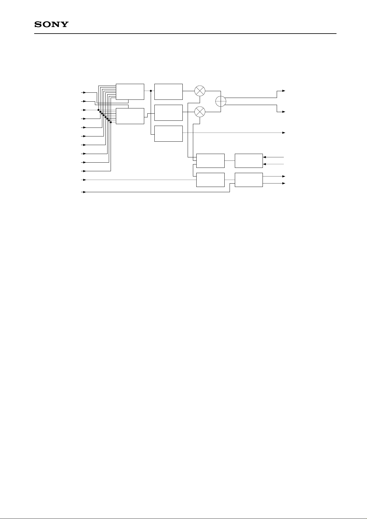
FM
· Built-in A/D convertor convert the RX base
band signal to the digital signal
· Analog output Receive Signal Strength
Indicator (RSSI) for CDMA
· Local Oscillator for I-Q mixer
• Transmit signal path includes:
· Built-in D/A convertor convert the digital I-Q
data to the analog baseband signal
· Built-in trim-free low-pass filter for CDMA and
FM
· Baseband to IF up-conversion
· Local Oscillator for I-Q mixer
· Built-in PLL for TX IF
• Built-in House keeping A/D convertor
• Low power consumption in all modes
• Single 3.3 V power supply
Absolute Maximum Ratings (Ta=25 °C)
• Supply voltage VCC –0.3 to 5.5 V
• Operating temperature Ta –55 to +125 °C
• Storage temperature Tstg –65 to +150 °C
Recommended Operating Conditions
• Supply voltage VCC 3.3±0.165 V
• Operating temperature Ta –40 to +85 °C
80 pin LQFP (Plastic)
Applications
• dual-mode CDMA/FM cellular telephone
Sony reserves the right to change products and specifications without prior notice. This information does not convey any license by
any implication or otherwise under any patents or other right. Application circuits shown, if any, are typical examples illustrating the
operation of the devices. Sony cannot assume responsibility for any problems arising out of the use of these circuits.
—1—
E96434-TE
Page 2

Block Diagram
CXA3003R
RXFMSTRB
FMCLK
RXQFMDT
RXIFMDT
DNC
DNC
GND ADC
VDD ADC
QOFFSET
IOFFSET
HKADVCC
NC
ADCCLK
ADCDT
ADCENBL
ADCIN
SLEEPB
IDLEB
FMB
RXVCOOUT
61
62
63
64
65
66
67
68
69
70
71
72
73
74
75
76
77
78
79
80
RXQD3
RXQD2
RXQD1
ADC
FMQ
RX LPF
FM Q
ADC
HK
CNTL
MODE
RXQD0
FMI
ADC
RX LPF
FM I
1/2
VCO
RXID3
CDMA Q
CDMA Q
RXID2
ADC
RX LPF
RXID1
CDMA I
CDMA I
RXID0
ADC
RX LPF
RSSI
CHIPX8
VDD BUF
Q DAC
CDMA Q
GND BUFF
5051535455565759 5860 41424344454647484952
TX LPF
TXCLKB
TX LPF
CDMA I
TXCLK
I DAC
TX LPF
FM
TXD7
TXD6
X8
CHIP
1/2
VCO
TXD5
TXD4
1/4
PLL
PD
TXD3
TXD2
TXD1
40
TXD0
39
GND ESD
38
VDD DAC
37
GND DAC
36
NC
35
NC
34
DNC
33
DNC
32
CAP2
31
CAP1
30
NC
29
TCXO4
28
NC
27
NC
26
TCXO
25
NC
24
LOCK DET
23
VDD TXF
22
GND TXF
21
VDD SYNTH
1 2 3 4 5 6 7 8 9
GND
RXVCO T1
RXVCO T2
VDD RXIF
GND RXIF
RXIFB
RXIF
RSSI
10 11 12 13 14 15 16 17 18 19 20
TXIF
TXIFB
VDD RX
GND RX
VDD TXIF
GND TXIF
FM MOD
TVCO T2
PD ISET
TVCO T1
—2—
PD OUT
GND SYNTH
Page 3

Pin Description
CXA3003R
Pin
No.
1
2
3
4
5
Symbol
GND
RXVCO TI
RXVCO T2
GND RXIF
VDD RXIF
Typical
Voltage (V)
DC AC
0 V
0 V
3.3 V
Equivalent circuit
2 3
1k 1k
Description
Negative power supply pin.
VDD RXIF
Receive VCO tuning pins.
Connected to an external LC
tank circuit for setting the
receive VCO frequency.
GND RXIF
Negative power supply pin for
RXIF block.
Positive power supply pin
for RXIF block.
VDD RXIF
6
7
8
RXIFB
RXIF
RSSI
2 V
2 V
2502k250
2k 2k
2k
GND RXIF
VDD RXIF
Analog differential receive IF
input pins.
Analog RSSI output pin.
6
7
150
8
9
10
GND RX
VDD RX
0 V
3.3 V
GND RXIF
Negative power supply pin for
RX block.
Positive power supply pin for
RX block.
—3—
Page 4
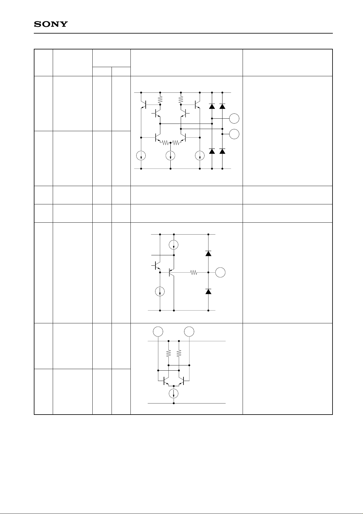
CXA3003R
Pin
No.
11
12
13
14
Symbol
TXIFB
TXIF
GND TXIF
VDD TXIF
Typical
Voltage (V)
DC AC
2.1 V
2.1 V
0 V
3.3 V
Equivalent circuit
400
200
400
200
VDD TXF
VDD TXIF
GND TXIF
Description
11
Analog differential transmit IF
12
output pins.
Negative power supply pin for
TXIF block.
Positive power supply pin for
TXIF block.
15
16
17
FM MOD
TVCO T1
TVCO T2
1.5 V
16 17
1k 1k
150
GND TXF
15
VDD TXIF
GND TXIF
Analog baseband signal output
pin for FM.
Transmit VCO tuning pins.
Connected to an external LC
tank circuit for setting the
transmit VCO frequency.
—4—
Page 5

CXA3003R
Pin
No.
18
19
Symbol
PD ISET
PD OUT
Typical
Voltage (V)
DC AC
0.64 V
Equivalent circuit
VDD TXF
150
GND TXF
VDD TXF
6.25k
150
19
18
Description
Current of PD OUT setting pin.
Transmit synthesizer charge
pump output pin.
20
GND SYNTH
21
VDD SYNTH
22
23
24
GND TXF
VDD TXF
LOCK DET
0 V
3.3 V
0 V
3.3 V
6.25k
VDD SYNTH
150
GND TXF
24
Negative power supply pin for
PLL block.
Positive power supply pin for
PLL block.
Negative power supply pin for
TX block.
Positive power supply pin for
TX block.
Transmit IF synthesizer lock
detect output pin.
GND SYNTH
—5—
Page 6
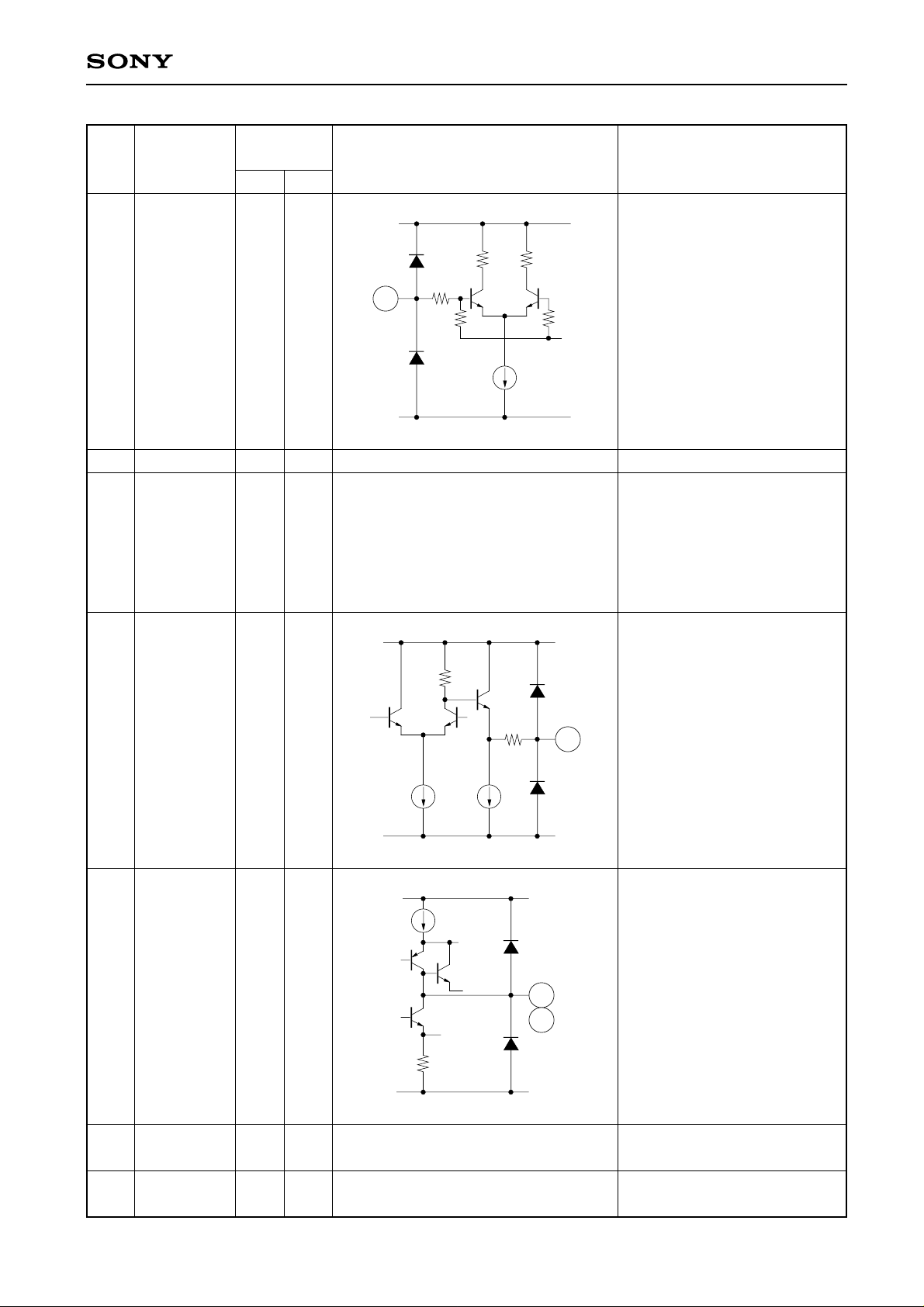
CXA3003R
Pin
No.
26
39
25
27
28
30
35
36
Symbol
TCXO
GND ESD
NC
Typical
Voltage (V)
DC AC
2.2 V
0 V
Equivalent circuit
150
26
20k 20k
Description
VDD SYNTH
Input pins for External clock
19.68 MHz (TCXO).
GND SYNTH
Negative power supply pin.
Don't connect pins.
29
31
32
TCXO4
CAP1
CAP2
VDD DAC
150
GND ESD
VDD RX
31
32
29
Output pin for TCXO/4
frequency.
The pins for External
Capacitor.
33
34
37
DNC
GND DAC
0 V
GND RX
Don't connect any line to this
pin.
Negative power supply pin for
TXDA block.
—6—
Page 7

CXA3003R
Pin
No.
38
40
to
47
48
49
50
51
Symbol
VDD DAC
TXD0
to
TXD7
TXCLK,
TXCLKB
GND BUF
VDD BUF
Typical
Voltage (V)
DC AC
3.3 V
0 V
3.3 V
Equivalent circuit
40
45
41
46
42
47
43
48
44
49
60k
Description
Positive power supply pin for
TXDA block.
VDD DAC
Transmit Data input pins for
Transmit 8 bit D/A converter.
TXD7 is the MSB.
Differential transmit Clock input
pins for Transmit 8 bit D/A
converter.
GND DAC
Negative power supply pin for
A/D output block.
Positive power supply pin for
A/D output block.
52
53
to
56
57
to
60
61
CHIP x 8
RXID0
to
RXID3
RXQD0
to
RXQD3
RXFMSTRB
61
62
100k
VDD BUF
GND BUF
VDD ADC
52
53
54
55
56
57
58
59
60
Output pin for CHIPx8 divider
with a ratio of
512/1025xTCXO.
Output pins for Receive
CDMA 4 bit A/D converter of I
signal. RXID3 is the MSB.
Output pins for Receive
CDMA 4 bit A/D converter of Q
signal. RXQD3 is the MSB.
Strobe input pin for Receive
FM 8 bit A/D converter.
62
FMCLK
Clock input pin for Receive FM
8 bit A/D converter.
GND ADC
—7—
Page 8
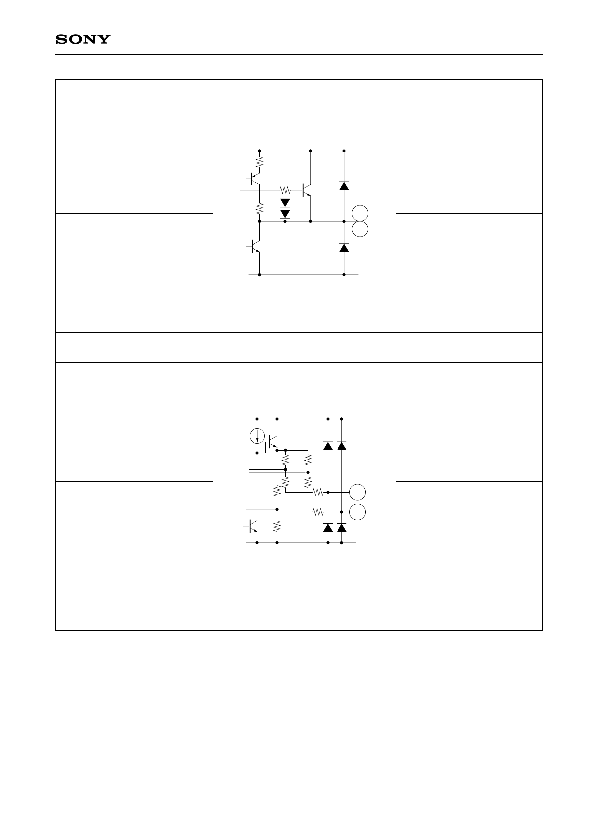
CXA3003R
Pin
No.
63
64
65
66
67
68
Symbol
RXQFMDT
RXIFMDT
DNC
GND ADC
VDD ADC
Typical
Voltage (V)
DC AC
0 V
3.3 V
Equivalent circuit
VDD BUF
GND BUF
Description
Q serial data output pin for
Receive FM 8bit A/D converter.
63
64
I serial data output pin for
Receive FM 8bit A/D converter.
Don't connect any line to this
pins.
Negative power supply pin for
A/D converter block.
Positive power supply pin for
A/D converter block.
69
70
71
72
QOFFSET
IOFFSET
HKADVCC
NC
1.5 V
1.5 V
3.3 V
22k
100k
30k
142k
30k
142k
150
150
VDD RX
GND RX
69
70
Receive Q channel offset
adjust input pin.
Receive I channel offset adjust
input pin.
Positive power supply pin for
HKA/D converter block.
Don't connect pin.
—8—
Page 9
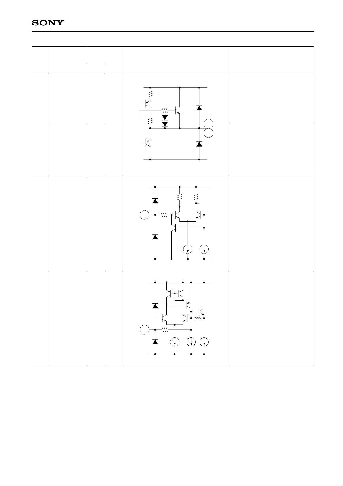
CXA3003R
Pin
No.
73
74
75
Symbol
ADCCLK
ADCDT
ADCENBL
Typical
Voltage (V)
DC AC
Equivalent circuit
60k
75
Description
VDD BUF
Clock output pin for House
Keeping 8 bit A/D converter.
73
74
Serial data output pin for
House Keeping 8 bit A/D
converter.
GND BUF
VDD BUF
Enable input pin for House
Keeping 8 bit A/D converter.
76
ADCIN
1.5 V
GND BUF
HKADVCC
A/D analog input pin for House
Keeping 8 bit A/D converter.
76
48.5k
GND ADC
—9—
Page 10
CXA3003R
Pin
No.
77
78
79
80
Symbol
SLEEPB,
IDLEB,
FMB
RXVCOOUT
Typical
Voltage (V)
DC AC
0 V
Equivalent circuit
77
78
79
150
VDD ADC
GND ADC
VDD RXIF
80
Description
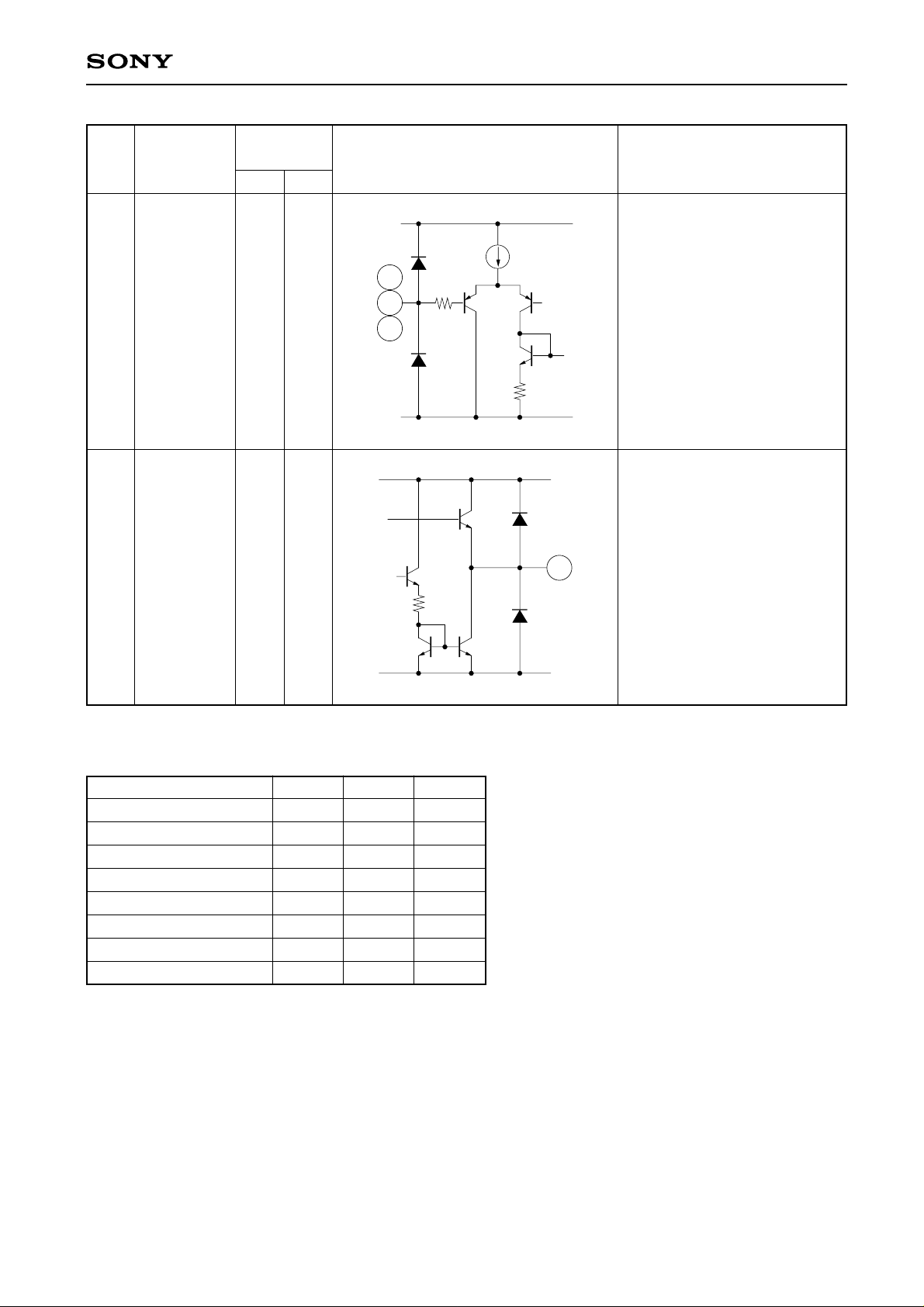
Test mode switch pins.
These pins control this IC
function mode (∗1).
Receive VCO output pin
connected the external PLL IC.
∗
1 Function Mode
Function Mode
CDMA RXTX
CDMA Idle
CDMA Sleep
FM RXTX
FM Idle
FM Idle (Transition)
FM RXTX (Transition)
CDMA Sleep (Transition)
FMB
high
high
high
low
low
low
low
high
IDLEB
high
low
low
high
low
low
high
high
SLEEPB
high
high
low
high
high
low
low
low
GND RXIF
Mode functions explain:
1. CDMA RXTX :
This mode requires everything except the FMspecific circuits to be operating.
2. CDMA Idle :
This mode powers down all transmit circuits
and FM receive.
3. CDMA Sleep :
This mode powers down everything except
the TCXO divider and TCXO/4 output driver.
4. FM RXTX :
This mode powers down all CDMA-specific
circuits except the CHIPx8 synthesizer.
5. FM Idle :
This mode powers down all transmit and
CDMA Receive circuits.
—10—
Page 11
CXA3003R
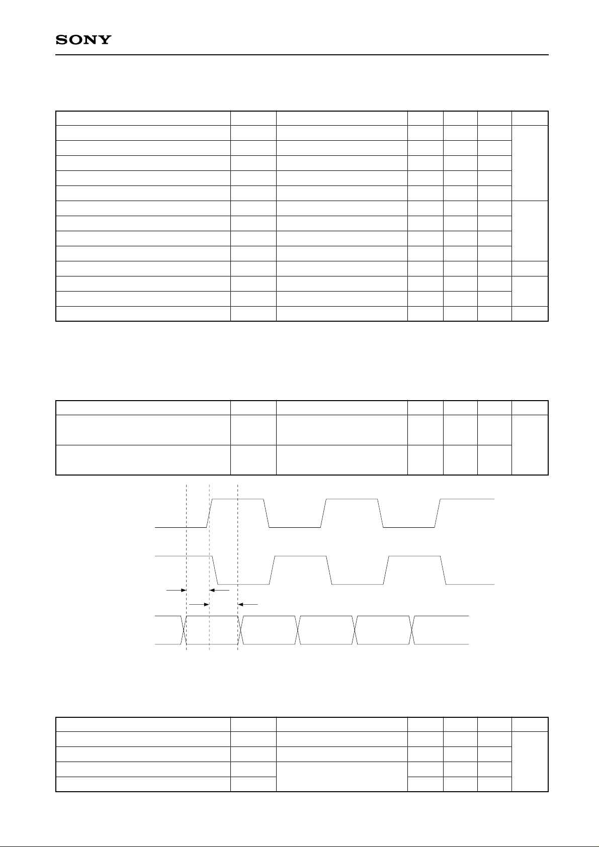
Electrical Characteristics
DC Characteristics (VDD=3.3 V±5 %, Ta=40 °C to 85 °C)
Item
Power supply current - CDMA RXTX
Power supply current - CDMA Idle
Power supply current - CDMA sleep
Power supply current - FM RXTX
Power supply current - FM Idle
Logic High level input voltage
Logic Low level input voltage
Logic High level output voltage
Logic Low level output voltage
Logic input Leakage current
Input capacitance Digital input
Load capacitance Digital output
Load resistance Digital output
∗
1 : Logic Input pins = 40, 41, 42, 43, 44, 45, 46, 47, 48, 49, 61, 62, 75, 77, 78, 79
Symbol
IDD1
IDD2
IDD3
IDD4
IDD5
VIH
VIL
VOH
VOL
IL
Cin-d
Cl-d
Rl-d
Condition
Min. Typ. Max. Unit
40 57
25 35
23mA
30 45
16 21
∗
1
∗
1
∗
1
∗
1
∗
1
∗
1
∗
1
∗
1
0.7xVDD
0.3xVDD
2.7
0.4
–100 100 µA
15
15
100 k Ω
pF
Logic Output pins =52, 53, 54, 55, 56, 57, 58, 59, 60, 63, 64, 73, 74
AC Characteristics
TXCLK/TXCLKB vs. TXIQDATA for CDMA mode VDD=3.3 V±5 %, Ta=–40 °C to 85 °C
Item
Data Setup to TXCLK/TXCLKB
Transition
Data Hold after TXCLK/TXCLKB
Transition
Symbol
tsua
tha
Condition Min. Typ. Max. Unit
50
ns
50
V
TXCLK
(input)
TXCLKB
(input)
tsua
tha
TXQDATA
(input)
TXCLK=4.9152MHz
TXQ Data TXI Data
Fig. 1 TXCLK/TXCLKB vs. TXIQDATA Timing Diagram for CDMA mode
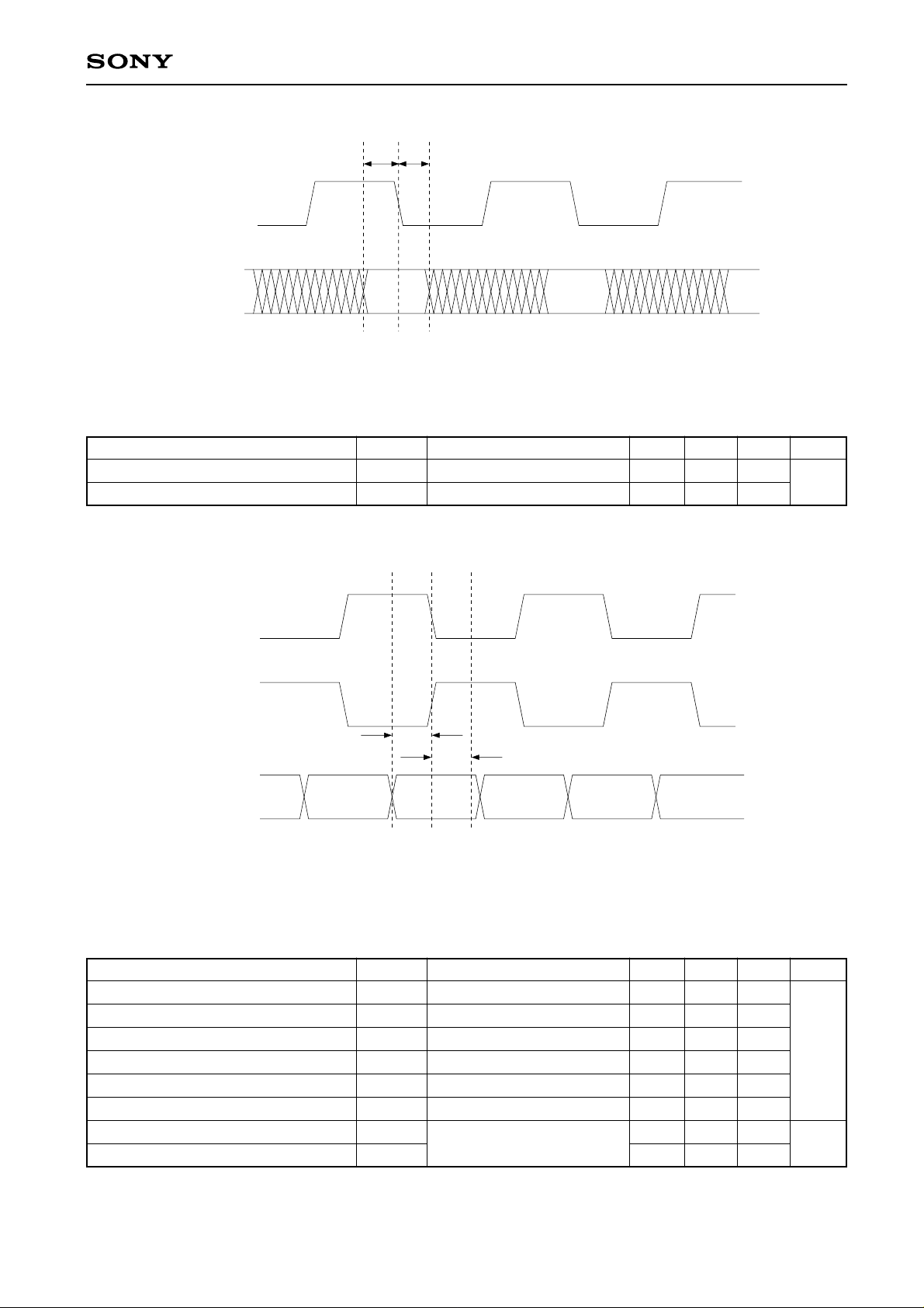
CHIPx8 vs. RXIQDATA VDD=3.3 V±5 %, Ta=–40 °C to 85 °C
Item
Data Output stable prior to CHIPx8 fall
Data Hold after CHIPx8 fall
CHIPx8 raise time
CHIPx8 fall time
Symbol
tsub
thb
trb
tfb
Condition
10 % to 90 %, Cload=15 pF
Min. Typ. Max. Unit
20
15
3 7.2
ns
3 9.9
—11—
Page 12
CXA3003R
tsub thd
Chip × 8
(output)
RXIData
RXQData
(output)
Fig. 2 CHIPx8 vs. RXIQDATA timing diagram
TXCLK vs. RXDATA for FM mode VDD=3.3 V±5 %, Ta=–40 °C to 85 °C
Item
Data setup to TXCLK transition
Data Hold after TXCLK transition
Symbol
tsuc
thc
Condition Min. Typ. Max. Unit
2.08
2.08
µs
TXCLK
(input)
TXCLKB
(input)
tsuc
thc
TX DATA
(input)
TXCLK=120kHz
XXXX XXXXTX Data XXXX
TX Data
Fig. 3 TXCLK vs. RXDATA mode timing diagram for FM
FMCLK, RXFMSTROBE vs. RXFMDATA (I, Q) VDD=3.3 V±5 %, Ta=–40 °C to 85 °C
Item
Strobe input valid to CLK Falling Edge
Strobe input valid after CLK Falling Edge
Data out valid to CLK Rising Edge
Data out valid after CLK Rising Edge
CLK High Time
CLK Low Time
RXFMDATA (I, Q) raise time
RXFMDATA (I, Q) fall time
Symbol
tsud-s
thd-s
tsud-d
thd-d
tclk-hi
tclk-lo
trd
tfd
Condition
10 % to 90 %, Cload=15 pF
Min. Typ. Max. Unit
0.69
2.08
1.38
1.38
µs
1.38
1.38
3 7.2
3 9.9
ns
—12—
Page 13
CXA3003R
FMCLK
(input)
FMRXSTROBE
(input)
FXRXDATA (I, Q)
(output)
LSB+1 LSB XXX MSB MSB-1 LSB
FMCLK=360kHz
FMRXSTROBE=40kHz
tclk-hi
tclk-lo tsud-d
thd-d thd-s
tsud-s
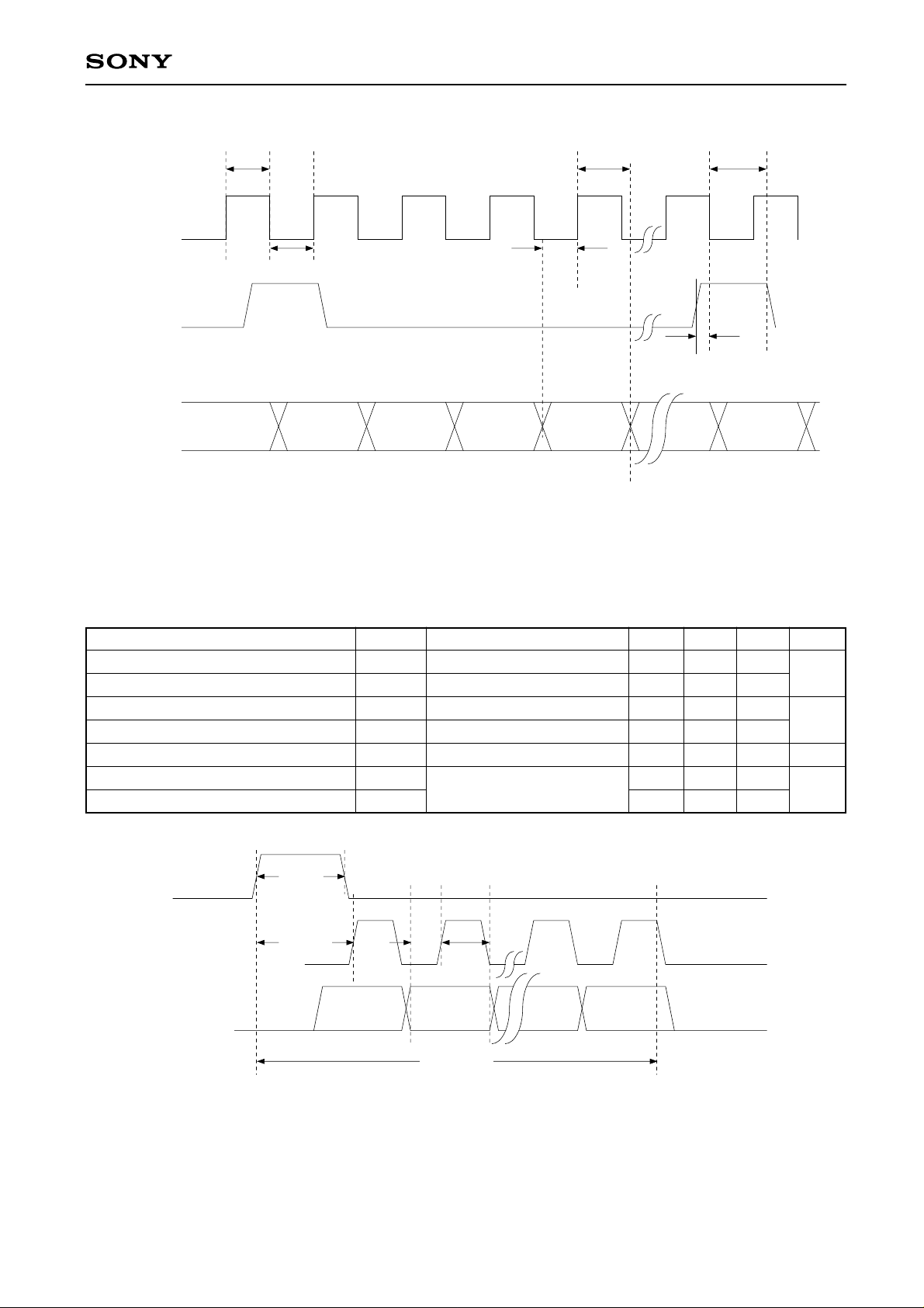
Fig. 4 FMCLK, FMRXSTROBE vs. RXFMDATA (I, Q) timing diagram
Note : FM RXSTROBE pulse width must be ≤ one FMCLK period.
ADCENABLE & ADC CLK vs. ADC DATA (VDD=3.3 V±5 %, Ta=–40 °C to 85 °C)
Item
Enable True to first Clock output
Enable Pulse to end of conversion
Data out valid to CLK rising edge
Data out valid after CLK rising edge
Enable True Pulse width
Output raise time
Output fall time
ADCENABLE
ADCCLK
ADCDATA
ten-pw
ten-clk
Symbol
Condition
ten-clk
tdEn-EOC
tsue-d
the-d
ten-pw
tre
tfe
MSB LSB
10 % to 90 %, Cl=15 pF
tsue-d
the-d
tdEn-EOC
Min. Typ. Max. Unit
6
16.8
600
600
µs
ns
10 µs
7.2
9.9
ns
ADCCLK=820kHz (TCXO÷24)
Fig. 5 ADCENABLE & ADC CLK vs. ADC DATA timing diagram
—13—
Page 14
CXA3003R
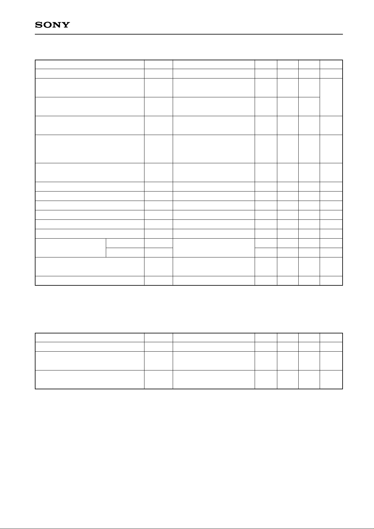
VHF Local Oscillator VDD=3.3 V±5 %, Ta=–40 °C to 85 °C
Item
VCO output Frequency Range
Lock mode charge pump Output
Current
Acquisition Mode charge pump
Output Current
Maximum Iout Adjustment Range
Acquisition Mode Disable Frequency
Range
Phase Detector Output Compliance
Voltage
Phase Detector Output Impedance
Reference Input Frequency
Phase Detector Frequency
Reference Spurs
Lock Detect Pull Down Voltage
Lock Detect Off Leakage Current
Phase Detect Unlock Deviation
Threshold during FM Rate
Tank Circuit Input Impedance
External VCO Input Levels
Symbol
fvcot
Icplt
Icpat
Icpmaxrt
∆fadt
Vopdt
Zopdt
freft
fpdt
rst
VLldt
ILedt
PDfhdt
PDfhrt
Zit
Vext
Condition
Rset=40 kΩ
Rset=40 kΩ
Using Rset to vary nominal
output current
Acquisition mode initiated
only by transition to any TX
active mode
Ref.frequency/16
Rload≥10 kΩ to VDD
VO=VDD
Measured at TXIF
Nominal Impedance into
each pin
Min. Typ. Max. Unit
260.76 MHz
12.4 15.5 18.6
µA
128 160 192
–40 +40 %
–1 k +1 k Hz
0.4
VDD–0.4
V
1 M 2 M Ω
19.68 MHz
1.23 MHz
–80 dBc
0.4 V
10 µA
12 kHz
300 Hz
1.5 k 2 k 2.5 k Ω
200 600 800 mVp-p
Receive VCO VDD=3.3 V±5 %, Ta=–40 °C to 85 °C
Item
VCO output Frequency Range
VCO Output Voltage
Swing at 170 MHz
Tank Circuit Input Impedance
Symbol
fvcor
Vovr
Zir
Condition
Into 500 Ω//5 pF load,
AC coupled load
Nominal impedance into
each pin
Min. Typ. Max. Unit
170.76 MHz
100 147 mVrms
1.5 k 2 k 2.5 k Ω
—14—
Page 15
CXA3003R
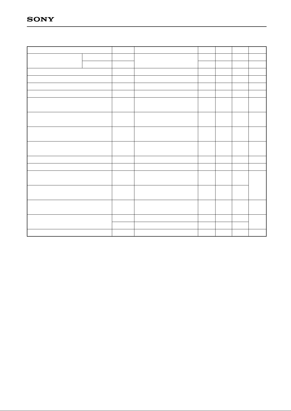
CDMA Receive VDD=3.3 V±5 %, Ta=–40 °C to 85 °C
Item
Input Signal Level CDMA
Sinusoid
Single Tone jammer Desense
Input Center Frequency
Input Resistance
Input Capacitance
Input Referred Noise
Spurious Content
Jammer Related Spurious Content
Offset Adjust Gain
Offset Adjust Input Impedance
A/D Converter Linearity
Signal Path Gain Accuracy,
Part to Part
Signal Path Gain Accuracy, Total
CDMA RX Residual Sideband
Product
Filter Attenuation
Gain Flatness vs. Frequency
Symbol
Vincdcr
Vinscr
Jdcr
ficcr
Ricr
Cicr
IRNcr
SCcr
Jrscr
Gadjocr
Ziocr
Ladcr
∆Gspcr
∆Gstcr
RSpcr
FA1cr
FA2cr
Gfcr
Condition
≥900 kHz offset
Differential
From each pin to GND
Sum of I&Q,measured from
1 kHz to 630 kHz
Total of all harmonic and
non-harmonic power
Peak in-band spurious
products
Full scale
At nominal temp and VDD
Over part to part,
VDD, temp
≥900 kHz
≥1.2 MHz
1 kHz to 630 kHz
Min. Typ. Max. Unit
0.9 mVrms
5.38 mVp-p
0.13 0.5 dB
85.38 220.38 MHz
375 500 650 Ω
1.5 pF
70 135 µVrms
–40 –25 dBc
–32 –18.4 dBc
–60 –50 –40
%Full
scale/V
100 k 170 k 220 k Ω
LSB
–1.6 1.6
dB
–2.1 2.1
21 dBc
46 50
48 62
dB
2.0 dBp-p
—15—
Page 16
CXA3003R
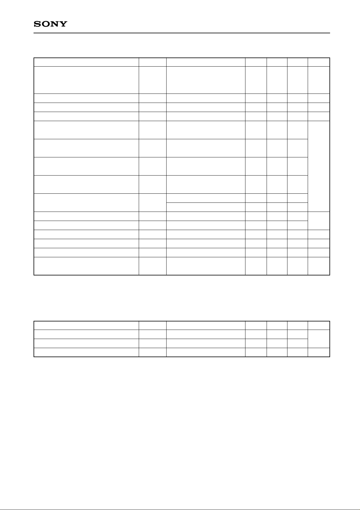
CDMA Transmit VDD=3.3 V±5 %, Ta=–40 °C to 85 °C
Item
Output Amplitude of Lower Sideband
Load Resistance
Load Capacitance
Output impedance
Spurious Free Dynamic Range,
In Band
Spurious Free Dynamic
Range,Bandedge
Spurious Free Dynamic Range,
Out of Band
Carrier Suppression
Spurious Free Dynamic Range
:IF Harmonics
Signal to Noise Ratio,Noise Band1
Signal to Noise Ratio,Noise Band2
Output Center Frequency
I, Q Gain Mismatch
I, Q Phase Imbalance
Amplitude Flatness vs. Frequency,
1 kHz to 630 kHz
Symbol
Voct
Rlct
Clct
Zoct
Sfdr1ct
Sfdr2ct
Sfdr3ct
Csct
Sfdr5ct
Snr1ct
Snr2ct
focct
Gerrct
Perrct
Afct
Condition
I&Q in Quadrature Full
Scale Signals.At nominal
VDD and temp
Differential
From each pin to GND
I&Q in Quadrature,
Full Scale Signals
Even Harmonics
Odd Harmonics
IF±≥0.1 M to IF±<1.98 M
IF±≥1.98 M to IF±<44 M
In band, Measured at TX IF
In band, Measured at TX IF
Including SIN(X)/X
Min. Typ. Max. Unit
267 300 337 mVp-p
495 500 505 Ω
5pF
40 50 Ω
35 50
30
dBc
57
18 32
20
811
104 124
117 124
dBc/Hz
130.38 MHz
0.2 0.8 dB
2 8 degree
0.6 1.0 dBp-p
CDMA CHIPX8 VDD=3.3 V±5 %, Ta=–40 °C to 85 °C
Item
Input Frequency
Output Frequency
Stabilization Time
Symbol
fic8
foc8
tsc8
Condition
TCXO
TCXO x 512/1025
upon mode charge
Min. Typ. Max. Unit
19.68
9.8304
MHz
10 µs
—16—
Page 17
CXA3003R
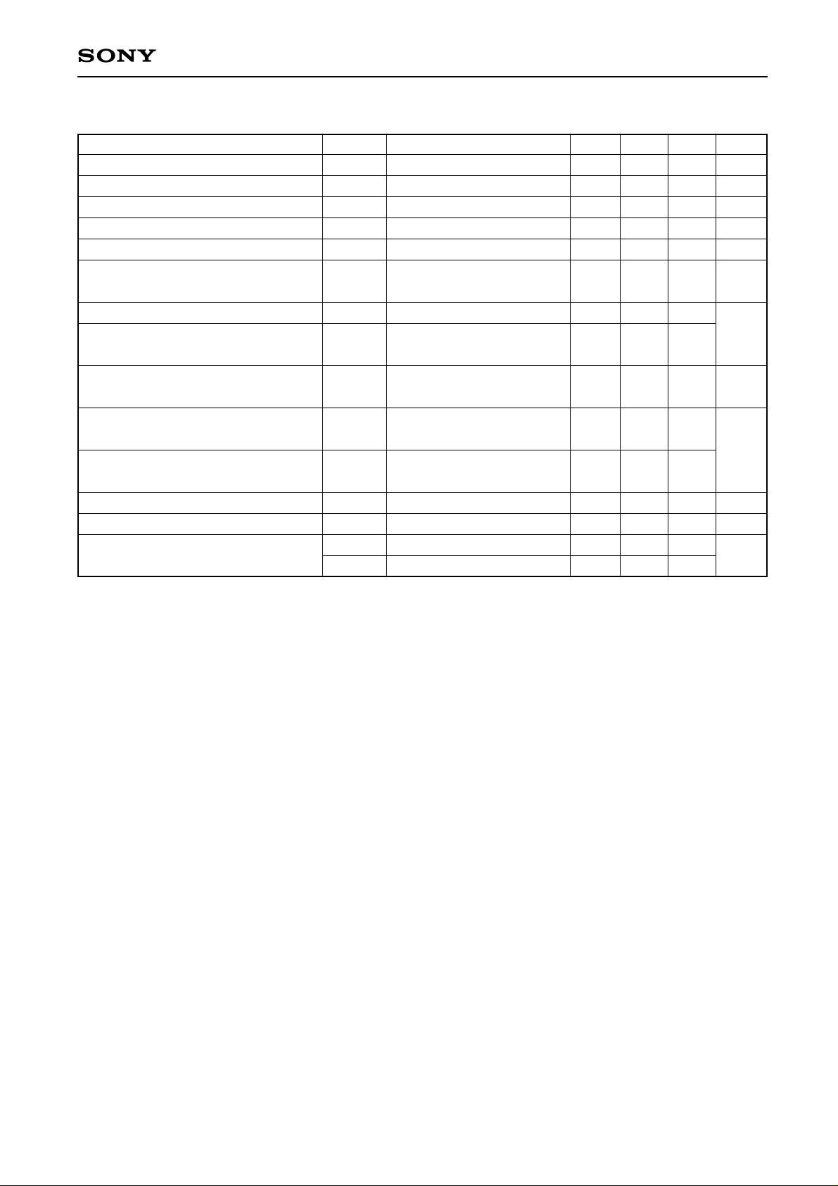
FM Receive VDD=3.3 V±5 %, Ta=–40 °C to 85 °C
Item
Input Signal Level
Single Tone jammer Desense
Input Center Frequency
Input Resistance
Input Capacitance
Input Referred Noise
Spurious Content
Jammer Related Spurious Content
Offset Adjust Gain
Signal Path Gain Accuracy,
Part to Part
Signal Path Gain Accuracy,Total
FM RX Residual Sideband Products
Gain Flatness vs. Frequency
Filter Attenuation
Symbol
Vinfr
Jdfr
ficfr
Rifr
IRNfr
SCfr
Jrfr
Gadjfr
∆Gspfr
∆Gspfr
∆Gstfr
RSpfr
Gffr
FA1fr
FA2fr
Condition
60 kHz offset
Differential
From each pin to GND
Sum of I&Q,measured
from 100 Hz to 15 kHz
At nominal temp
Peak in-band spurious
product
At nominal VDD and temp
Over part to part ,VDD,
temp
From 100 Hz to 12.2 kHz
>45 kHz
>60 kHz
Min. Typ. Max. Unit
1.53 mVrms
0.07 0.35 dB
85.38 MHz
375 500 650 Ω
1.5 pF
38 µVrms
–56 –42 dBc
–32 –18.4
–60 –50 –40
%Full
scale/V
–1.3 1.3
dB
–2.1 2.1
27 dBc
0.4 1 dBp-p
48 68
60 69
dB
—17—
Page 18
CXA3003R
FM Transmit VDD=3.3 V±5 %, Ta=–40 °C to 85 °C
Item
IF Output Amplitude
IF Load Resistance
IF Load Capacitance
IF Output impedance
IF Signal to Noise Ratio,
Noise Band1
IF Output Amplitude Variation
IF Output Amplitude Drift
Maximum Spurious Content
: TX IF Harmonics
FM Mod Output Voltage
FM Mod load Resistance
FM Mod Amplitude Variation
FM Mod Spurious Free Dynamic
Range, to 120 kHz
FM Mod Signal to Noise Ratio,
1 kHz to 15 kHz
Amplitude Flatness vs. Frequency,
DC to 10 kHz
Symbol
Voifft
Rlifft
Clifft
Zoft
Snr1ft
Voifvft
∆Voifdft
Sceft
Scoft
Vmodft
Rmodft
∆Vmodvft
Sfdrft
Shrfmodft
Afft
Condition
At nominal VDD and temp
Differential
From each pin to GND
IF±≥0.1 M to IF±<44 M
Over part to part ,
VDD and temp
Over full VDD and
temp ranges
Even Harmonics
Odd Harmonics
Full scale, nominal VDD
and temp
Over part to part ,
VDD and temp
Two tone inputs
Single tone, full scale
Including SIN (X) / X
Min. Typ. Max. Unit
124 140 161 mVp-p
495 500 505 Ω
5pF
40 50 Ω
110 117 dBc/Hz
–1.6 1.6
dB
–1 1
–20
–10.5 –8
dBc
490 575 610 mVp-p
10 k Ω
–1.2 1.2
dB
40 44
87 100 dBc/Hz
0.6 dBp-p
TCXO VDD=3.3 V±5 %, Ta=–40 °C to 85 °C
Item
Input Frequency
Input Amplitude
Input Impedance
TCXO Divide Ratio
TCXO / 4 Output Amplitude
Symbol
fitc
Vitc
Zitc
Rtdtc
Vo-tc
Condition
From TCXO
AC Coupled
Into 10 kΩ // 10 pF
AC coupled Load
Min. Typ. Max. Unit
19.68 MHz
0.5 2 Vp-p
5 k Ω
4
1 Vp-p
—18—
Page 19

CXA3003R
RSSI VDD=3.3 V±5 %, Ta=–40 °C to 85 °C
Item
Dynamic Range
Gain
Gain Drift
Output Signal Level
Output Load Resistance
Full Scale Rise/Fall Time
Nominal Setpoint
Symbol
DRrs
Grs
∆Gdrs
Vors
Rlrs
trrs/tfrs
Nsprs
Condition
At nominal temp and VDD
Over VDD and Temp
At nominal temp and VDD
Min. Typ. Max. Unit
25 dB
32 75 mV/dB
–1.6 1.6 dB
0.5 2.5 V
50 k Ω
30 µs
0.8 2.0 V
HK ADC VDD=3.3 V±5 %, Ta=–40 °C to 85 °C
Item
Resolution
Input Voltage Range
Midscale Output Code Error
DLE
ILE
Conversion Time
Input Impedance
Symbol
Reshk
Vihk
Emidhk
Dlehk
Ilehk
tchk
Zihk
Condition
Internal Voltage referenced
V (ADCIN)=1.5 V
At nominal temp and VDD
Min. Typ. Max. Unit
8 Bits
1.79 2 2.24 V
–16 16 code
–1 1
–1.25 1.25
LSB
40 µs
20 k Ω
—19—
Page 20
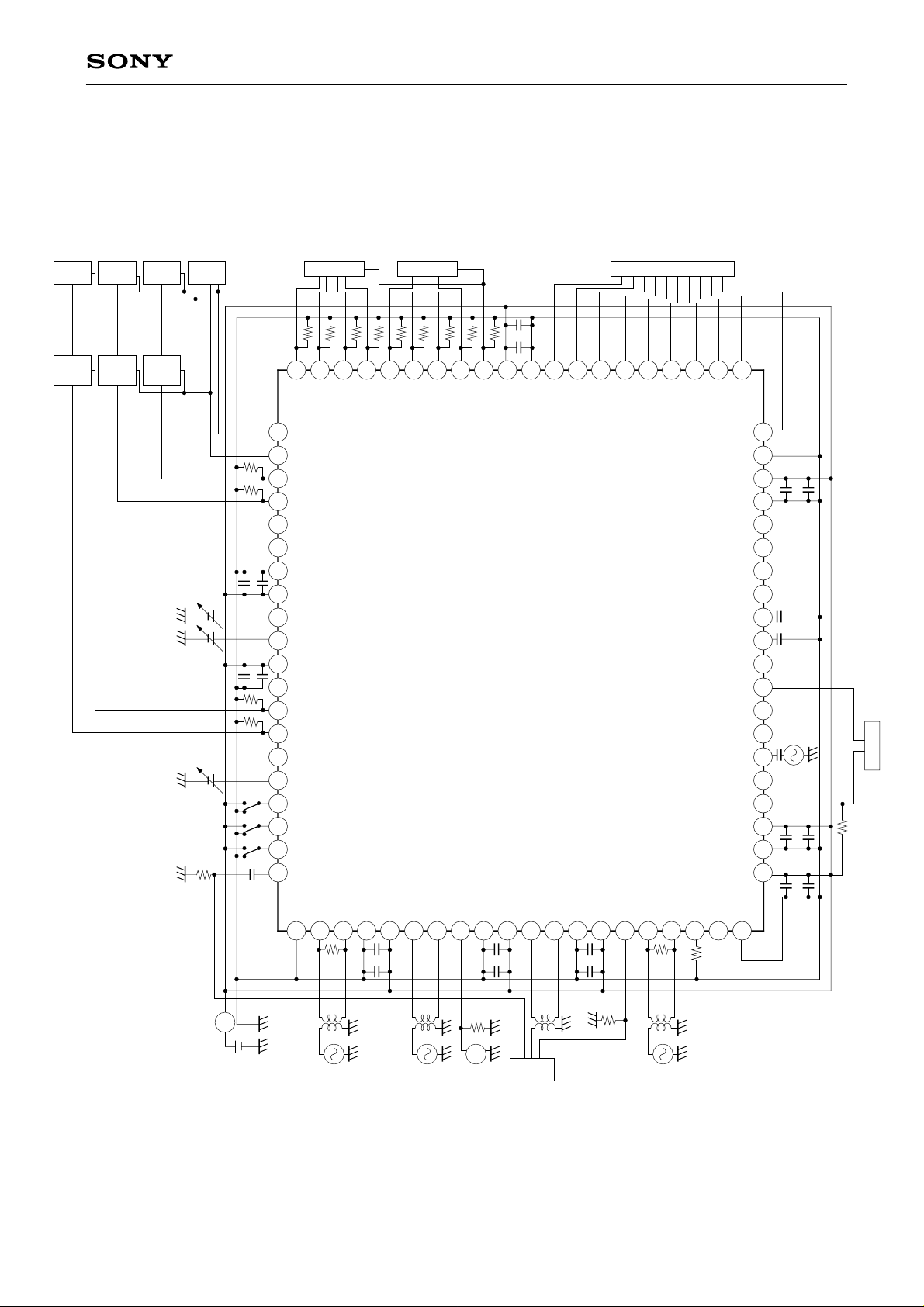
Electrical Characteristics Measurement Circuit
Pattern
D/A
D/A
D/A
converter
SerialParallel
Converter
converter
SerialParallel
Converter
converter
SerialParallel
Converter
Generator
500
100k
100k
1n
0.01µ
1n
0.01µ
100k
100k
100p
D/A converter D/A converter Pattern Generator
100k
61
62
63
64
65
66
67
68
69
70
71
72
73
74
75
76
77
78
79
80
100k
RXQD3
RXFMSTRB
FMCLK
RXQFMDT
RXIFMDT
DNC
DNC
GND ADC
VDD ADC
QOFFSET
IOFFSET
HKADVCC
NC
ADCCLK
ADCDT
ADCENBL
ADCIN
SLEEPB
IDLEB
FMB
RXVCOOUT
GND
1
100k
RXQD2
RXQD1
RXVCO T1
RXVCO T2
2 3 4 5 6 7 8 9
50 50
100k
100k
RXID3
RXQD0
GND RXIF
VDD RXIF
1n
100k
RXID2
RXIFB
100k
RXID1
RXIF
1n
100k
100k
0.01µ
5051535455565759 5860 41424344454647484952
TXD7
TXD6
RXID0
CHIPX8
VDD BUF
TXCLKB
GND BUFF
TXCLK
TXD5
CXA3003R
RSSI
GND RX
VDD RX
TXIFB
TXIF
VDD TXIF
GND TXIF
FM MOD
TVCO T2
10 11 12 13 14 15 16 17 18 19 20
0.01µ0.01µ
1n
0.01µ
1n
TXD4
TVCO T1
TXD3
TXD2
TXD0
GND ESD
VDD DAC
GND DAC
DNC
DNC
CAP2
CAP1
TCXO4
TCXO
LOCK DET
VDD TXF
GND TXF
VDD SYNTH
PD ISET
PD OUT
39k
NC
NC
NC
NC
NC
NC
GND
TXD1
SYNTH
40
39
38
37
36
35
34
33
32
31
30
29
28
27
26
25
24
23
22
21
CXA3003R
1n
0.01µ
0.01µ
0.01µ
1n
1n
0.01µ
1n
0.01µ
Oscilloscope
10k
A
1:1
1:3
51k
1:1
V
Spectrum
Analyzer
10k
1:1
—20—
Page 21
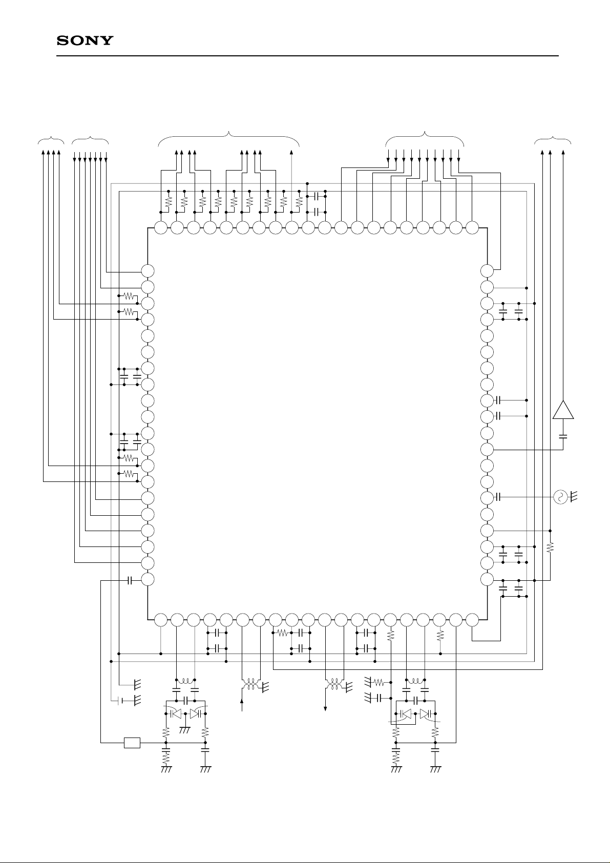
Application Circuit
CXA3003R
To Digital
Processing
section
From Digital
Processing
section
100k
100k
To Digital
Processing section
100k
100k
100k
100k
100k
100k
100k
1n
0.01µ
From Digital
Processing section
To Digital
Processing section
5051535455565759 5860 41424344454647484952
TXD5
TVCO T2
TXD4
TVCO T1
TXD3
PD ISET
TXD7
RXID1
RXIF
RXID0
CHIPX8
VDD BUF
GND BUFF
TXCLKB
TXCLK
CXA3003R
RSSI
GND RX
VDD RX
TXIFB
TXIF
GND TXIF
10 11 12 13 14 15 16 17 18 19 20
51k
0.01µ
1n
RXID3
RXQD3
RXQD2
RXFMSTRB
61
FMCLK
62
100k
RXQFMDT
63
100k
RXIFMDT
64
DNC
65
DNC
66
GND ADC
67
1n
0.01µ
VDD ADC
68
QOFFSET
69
IOFFSET
70
HKADVCC
71
1n
0.01µ
NC
72
100k
ADCCLK
73
100k
ADCDT
74
ADCENBL
75
ADCIN
76
SLEEPB
77
IDLEB
78
FMB
79
100p
80
RXVCOOUT
GND
RXVCO T1
2 3 4 5 6 7 8 9
1
RXQD0
RXQD1
GND RXIF
RXVCO T2
0.01µ 0.01µ
1n
RXID2
VDD RXIF
RXIFB
TXD6
VDD TXIF
FM MOD
22k 39k
1n
TXD2
TXD0
GND ESD
VDD DAC
GND DAC
DNC
DNC
CAP2
CAP1
TCXO4
TCXO
LOCK DET
VDD TXF
GND TXF
VDD SYNTH
PD OUT
NC
NC
NC
NC
NC
NC
TXD1
GND
40
39
38
37
36
35
34
33
32
31
30
29
28
27
26
25
24
23
22
21
SYNTH
0.01µ
0.01µ
0.01µ
1n
0.01µ
0.01µ
1n
Amp
1n
1n
1n
100n
56p 56p
1T367 1T367
10k 10k
PLL
2p
From Receive
RF Circuits
To Transmit
RF Circuits
220
680p
1T367 1T367
10k 10k
0.86µ
1.8k
47n
22p 22p
8p
1n
Application circuits shown are typical examples illustrating the operation of the devices. Sony cannot assume responsibility for
any problems arising out of the use of these circuits or for any infringement of third party patent and other right due to same.
—21—
Page 22

Description of Operation
1. Overall operations
This IC bridges the gap between the analog RF processing and digital processing sections of the cellular
telephone. Figure 6 illustrates the general circuit blocks in the portable cellular telephone employing this
IC. The analog inputs and outputs of this IC interface directly with the IF (intermediate frequency)
transmit/receive circuitry of the telephone. The digital inputs and outputs of this IC interface directly with
the digital processing section.
The RF receive circuitry acquires the low-level forward link signal from the base station (cell site) and
down-converts to the IF frequency band. The RF transmit circuitry takes CDMA or FM modulated analog
IF from this IC, up-converts to the channel frequency, and outputs controlled reverse link power levels to
the antenna.
The digital processing section includes CDMA modulation/demodulation , digital FM
modulation/demodulation, voice processing, and a keypad interface. The CODEC (coder-decoder) block
interfaces the telephone microphone and earpiece to the digital processing section.
This IC receive signal path down-converts the acquired IF signal to baseband where it is then converted
to digital data. The digital baseband signals are sent to the digital processing section for demodulation.
When transmitting, the digital processing section sends modulated digital baseband signals to this IC for
up-conversion to the analog IF frequency.
This IC consists of a receive signal path, a transmit signal path, clock synthesis and buffering circuits,
mode control logic, and a House Keeping analog-to-digital converter (ADC).
CXA3003R
Antenna
RF
Transmit/
Receive
Processing
The digital processing
Mobile Station Modem
CXA3003R
Baseband
Analog
Processor
CODEC
Fig. 6 Dual-mode CDMA/FM cellular Telephone Block
2. CDMA Receive Signal Path
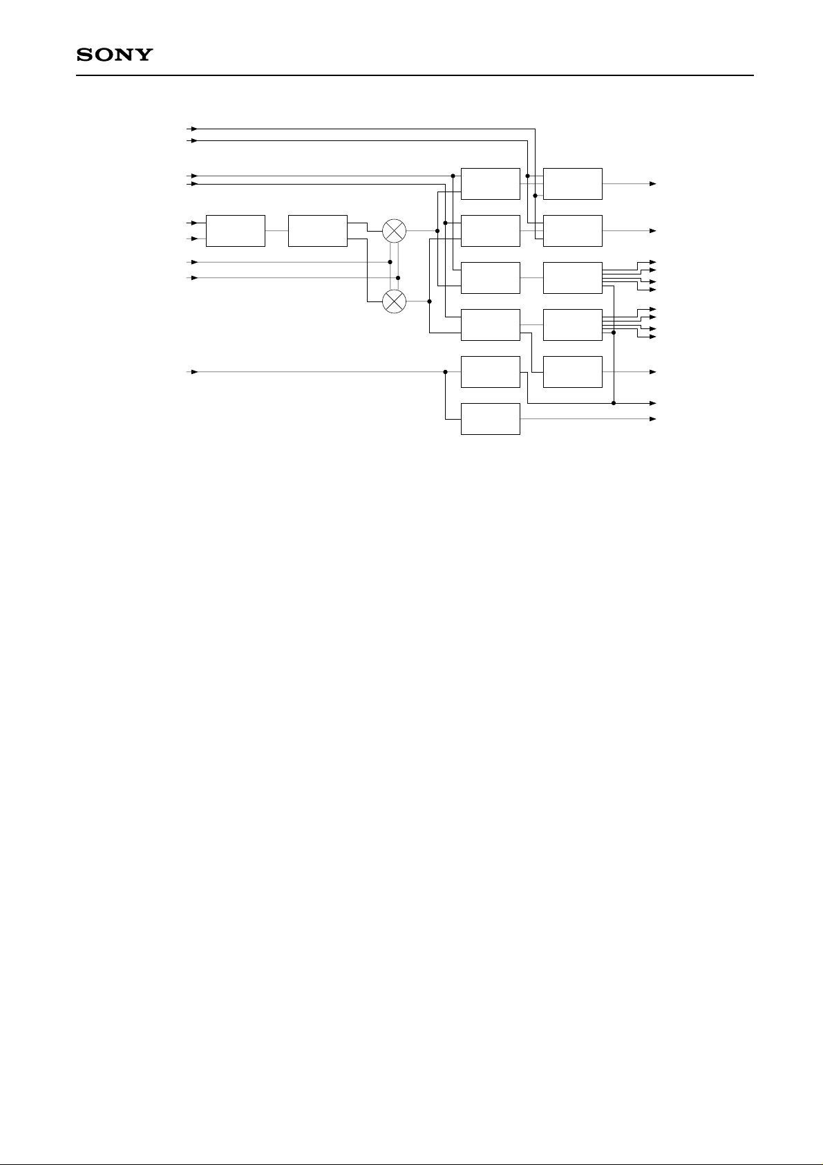
This IC receive signal path (see Fig.7) is designed to accept a differential IF signal with CDMA spread
spectrum modulation extending ±630 kHz from the IF center frequency of 85.38 MHz. The incoming IF is
reduced to I and Q baseband components by mixing with 85.38 MHz local oscillator (LO) signals in
quadrature followed by low-pass filtering.
The 85.38 MHz I and Q LO signals are generated on this IC. The receive VCO is set 170.76 MHz by an
external varactor-tuned resonant tank circuit (inductor L and capacitor C connected in parallel). An
external phase-lock loop and loop filter network provide the feedback to the varactors which tune the VCO
to 170.76 MHz. A master-slave divide-by-two circuit generates I and Q signals in precise quadrature for
the mixers.
—22—
Page 23
RXFMSTROBE
FMCLK
CXA3003R
QOFFSET
IOFFSET
RXVCO T1
RXVCO T2
RXIFB
RXIF
TCXO
1/2VCO
FM Q
RX LPF
FM I
RX LPF
CDMA Q
RX LPF
CDMA I
RX LPF
CHIP
X8
1/4
FM Q
ADC
FM I
ADC
CDMA Q
ADC
CDMA I
ADC
RSSI
RXQFMDATA
RXIFMDATA
RXQD3
RXQD2
RXQD1
RXQD0
RXID3
RXID2
RXID1
RXID0
RSSI
CHIPX8
TCXO4
Fig. 7 Receive Section Block Diagram of CXA3003R
3. CDMA Low-Pass Filtering
After mixing, the receive signal path splits into CDMA and FM sections. For CDMA, the baseband signal
extends from 1 kHz to 630 kHz. Frequency components above 750 kHz are out-of-band for CDMA
operation. The mixers and the subsequent CDMA low-pass filters combine to form the down-converter
which outputs the CDMA baseband signals. The passband, transition band, and rejection band
characteristics of these low-pass filters, in conjunction with external IF bandpass filtering, contribute to the
ability of the receiver to select the desired baseband signals from the jamming effects of unwanted
signals.
The need to control the offset at the inputs of the ADCs is critical to the receive signal path and the digital
processing section. The offset control inputs : IOFFSET and QOFFSET, are provided for this purpose.
4. CDMA Analog-to-Digital Conversion
Analog I and Q baseband components are converted to digital signals by the two identical
4-bit flash (parallel) ADCs. The CDMA ADCs output a new digital value on each falling edge of the ADC
clock signal, CHIPx8.
The CHIPx8 ADC clock frequency of 9.8304 MHz is synthesized from the system crystal oscillator
frequency of 19.68 MHz. The system crystal oscillator frequency is applied to the TCXO input of this IC.
5. FM Receive Signal Path
The receive signal path for FM operation is similar to that for CDMA operation. Differences lie in the
characteristics of the I and Q low-pass filters and the ADCs. The IF frequency is the same as in CDMA
(85.38 MHz), but the modulation can only extend ±15 kHz from the IF center frequency, forming a 30 kHz
wide channel. The low-pass filters for FM operation have a much lower bandwidth than those used in
CDMA. The offset of the FM low-pass filters is controlled just like the CDMA low-pass filters by the
IOFFSET and QOFFSET input pins.
The lower bandwidth of the FM baseband signal gives rise to the use of very low power 8-bit successiveapproximation ADCs. The FM I and Q analog baseband signals are sampled and held during the analog
to digital (A/D) conversion process. The A/D conversion is initiated with a external strobe signal. A serial
data stream is output beginning with the most significant bit (MSB) of the result.
—23—
Page 24
CXA3003R
6. CDMA Transmit Signal Path
This IC transmit signal path (see Fig.8) accepts digital I and Q baseband data from the digital processing
section and outputs modulated IF centered at 130.38 MHz to the RF transmitter.
TXCLKB
TXCLK
TXD7
TXD6
TXD5
TXD4
TXD3
TXD2
TXD1
TXD0
TCXO
PD ISET
Q DAC
I DAC
CDMA Q
TX LPF
CDMA I
TX LPF
FM
TX LPF
1/2 VCO
PLL PD
TXIFB
TXIF
FM MOD
TVCO T2
TVCO T1
PD OUT
LOCK DET
Fig. 8 Transmit Section Block Diagram of CXA3003R
7. CDMA Digital to Analog Conversion and Filters
Eight bits of I and Q transmit data are input to the CDMA digital to analog converters (DACs) by
multiplexing over an 8-bit input port on the this IC. The transmit data rate is twice as fast as the
differential transmit clock, TXCLK and TXCLKB. Incoming data that is valid during the rising edge of the
transmit clock is registered into the I DAC. Incoming data that is valid during the falling edge of the
transmit clock is registered into the Q DAC. I and Q transmit data values have been compensated in the
digital processing section to account for their 1/2 clock cycle time difference.
The frequency spectrum at the output of the CDMA DACs contains unwanted frequency components due
to DAC output transition edges and transients. The transmit clock frequency and harmonics are found in
the spectrum and are also undesirable. Each CDMA DAC is followed by an anti-aliasing low-pass filter
with a bandwidth of 630 kHz that reduces unwanted frequency components. Unlike the low-pass filters in
the receive signal path, these do not require offset controls.
8. Up-Converting to IF
This IC transmit path outputs a differential IF signal with CDMA spread spectrum modulation extending
±630 kHz from the transmit IF center frequency of 130.38 MHz. The analog I and Q baseband
components from the CDMA low-pass filters are mixed in quadrature with I and Q LO signals at 130.38
MHz. After mixing, the I and Q IF components are summed and output differentially.
The 130.38 MHz I and Q LO signals are generated on this IC. The transmit VCO is set to 260.76 MHz by
an external varactor-tuned resonant tank circuit. An internal phase-lock loop and external loop filter
network provides the feedback to the varactors which tune the VCO precisely to 260.76 MHz. A masterslave divide-by-two circuit generates I and Q signals in precise quadrature for the mixers.
—24—
Page 25

CXA3003R
9. FM Transmit Signal Path
An analog FM modulation signal is constructed from 8-bit digital data supplied by the digital processing
section. Only the Q-channel DAC is used in this IC in FM mode, all other CDMA circuits are disabled.
The DAC output is filtered by a low-pass anti-aliasing filter. The filtered DAC output is the analog FM
modulation signal, FM MOD. This signal modulates the frequency of this IC transmit VCO using external
components when in FM RXTX Mode.
10.Operating Modes
This IC has several modes of operation. The CDMA RXTX or FM RXTX modes are in effect when the
telephone is making a call. IDLE mode is in effect when no call is in progress but the telephone receiver
is active (ready to answer a call). SLEEP mode is a low-power mode in which the telephone cannot
receive a call.
This IC operating modes are defined by the states of three digital inputs: FMB, IDLEB, and SLEEPB. The
power consumed by this IC is minimized by controlling these logic signals and disabling unused circuits.
The selected circuits in this IC become active after the states of the operating mode controls are changed.
11.House Keeping ADC
The House Keeping ADC provides DC measurement capability to the telephone. It is a low speed, 8-bit
resolution, successive approximation analog-to-digital converter. It is designed to digitize DC voltages
applied to the ADCIN pin from battery level, temperature, and other low frequency control or monitoring
sensors.
This ADC is in a power-down state during normal operation. It is activated by a positive-going pulse on
ADCENBL. When this input is driven high, the House Keeping ADC powers up, samples and holds the
voltage applied to ADCIN, and begins a conversion. The ADC output is available from a serial digital
interface. Each of the eight data bits is valid (MSB first) during the rising edge of the ADCCLK output. A
rising edge of ADCENBL during a conversion will be ignored. ADCENBL must be low and a conversion
completed before a new conversion can be started.
—25—
Page 26
Notes of Operation
1. Signal operation
The CXA3003R needs the master system clock “TCXO” that comes from a crystal oscillator at 19.68
MHz. A divide-by-4 derivative of TCXO called TCXO/4 operates as long as TCXO is active and power is
applied to CXA3003R. Transmit and receive IF frequencies are generated by varactor-tuned TX and RX
local oscillators on CXA3003R. CHIPx8, a derivative of TCXO is active for all operating modes except
CDMA SLEEP and FM IDLE.
2. Receive IF Inputs
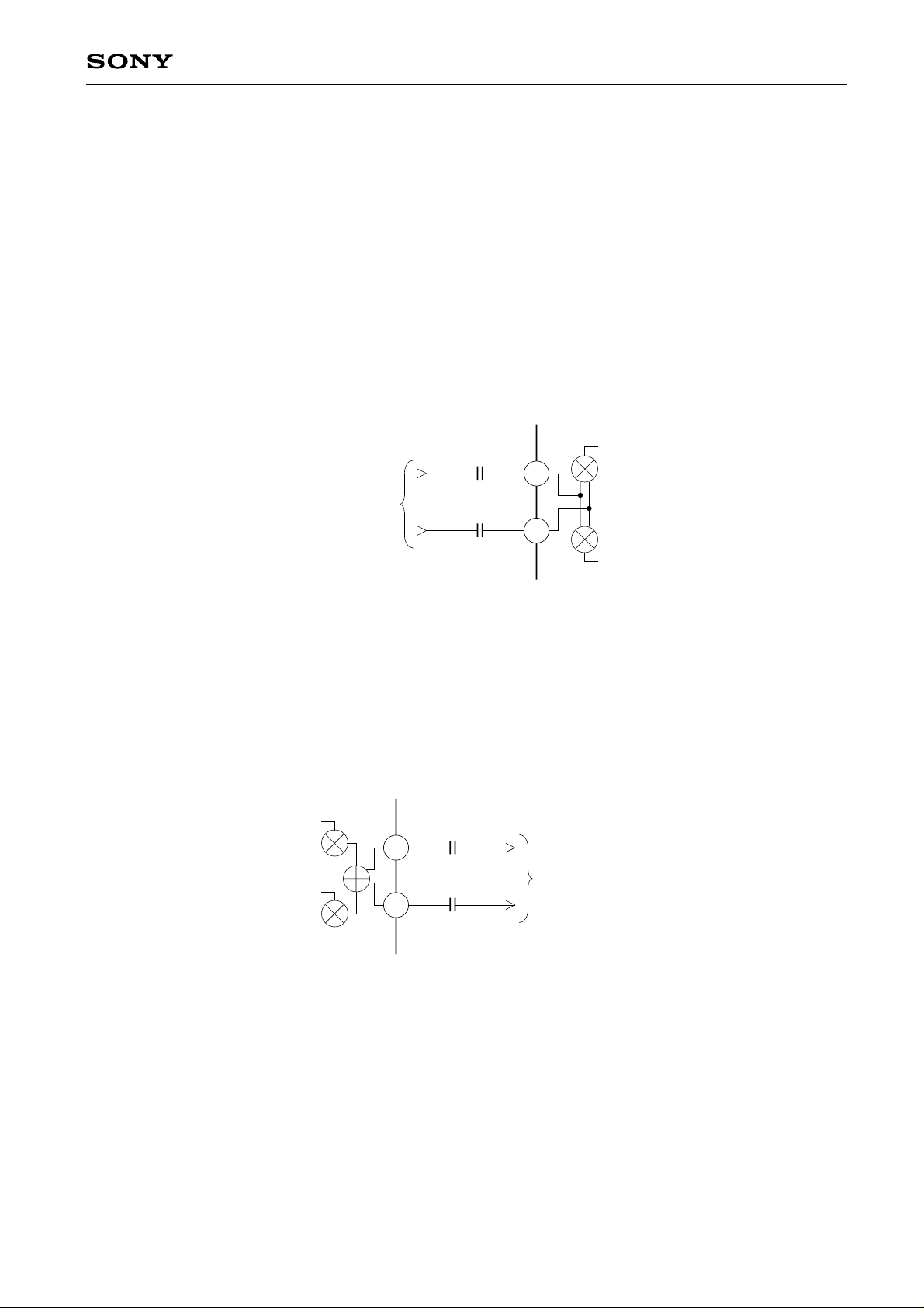
The receive IF inputs, RXIF and RXIFB, differentially drive a input stage within the CXA3003R. The
differential input impedance is nominally 500 Ω. The IF signals receive by AC coupling. AC coupling
capacitor values (0.001 µF) are chosen to maximize the power transfer from receive IF circuitry.
CXA3003R
6
From Receive
RF Circuits
7
CXA3003R
Fig. 9 Receive IF Inputs
3. Transmit IF Outputs
The transmit IF outputs, TXIF and TXIFB, are differential outputs. The output impedance is low, 40 Ω,
nominally. These signals transfer to the subsequent transmit IF circuitry by using AC coupling. AC
coupling capacitor values (0.001 µF) are chosen to maximize the power transfer from the CXA3003R to
the subsequent transmit IF circuitry.
CXA3003R
11
To Transmit
RF Circuits
12
Fig. 10 Transmit IF Outputs
—26—
Page 27
4. VCOs
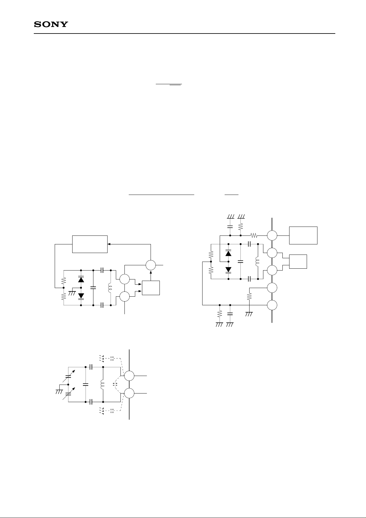
In general terms, the frequency of oscillation, fo, for the VCOs is determined by:
CXA3003R
fo =
1
2 π√LC
Where L and C are the net inductance and Capacitance of the external resonant tank circuit. The
resonant tank circuit comprises inductor L connected in parallel with capacitance C. The tank circuit is
connected between RXVCO T1 and RXVCO T2 (shown in Fig.11). Another tank circuit is connected
between TXVCO T1 and TXVCO T2 (shown in Fig.12).
The net capacitance of the tank circuit comprises a varactor diode (CV), an optional scaling capacitor
connected (CV2) in parallel with the varactors, two DC blocking capacitors (CB) isolating the DC bias of
the varactors from the CXA3003R, and pin-to-pin and pin-to-ground parasitic capacitors (CPP, CPG)
(shown in Fig.13). The net tank capacitance is found from
External PLL
Circuit
C=
(CV2 + 1/2 · CV) × CB
(CV2 + 1/2 · CV) × 2 + CB 2
80
2
OSC
3
CXA3003R
+ (CPP +
CPG
)
40k
15
16
17
18
19
FM TX LPF
VSC
CXA3003R
Fig. 11 Receive VCO Fig. 12 Transmit VCO
CPG
CB
C
PP
CV
CV
L
CV2
CXA3003R
CB
CPG
Fig. 13 VCO capacitors
5. Transmit VCO Synthesizer
The transmit synthesizer consists of a VCO, a divide-by-two phase splitter, divide by R and N counters,
and a phase detector. The VCO and divide-by-two generate the I and Q IF signals used to up-convert
analog baseband to IF. The loop filter and tuning components are external to the CXA3003R.
—27—
Page 28

CXA3003R
LO
PD OUT
VCO
Phase
Detector
Reference
Divider
n=16
Divider
1/2
Divider
1/106
19.68MHz from TCXO
to TX Modulator
Fig. 14 Transmit VCO synthesizer
6. Transmit VCO Phase Detector
The phase detector output, PD OUT, is the output of a dual mode bi-directional charge pump. It provides
two levels of output current for frequency acquisition (±175 µA) and phase lock maintenance (±16 µA)
after the VCO frequency is at or near its final frequency. The phase detector also provides a lock detect
output, LOCK. This signal is low when unlocked, and high (high-impedance) when unused or in IDLE or
SLEEP Modes. LOCK will indicate the unlocked condition until the VCO frequency is at its final value.
LOCK will then toggle until phase lock has been established.
The current available from PD OUT is set by an external resistor connected between PD ISET and
ground (shown in Fig. 12). The value of the PD ISET resistor is determined by
RPD = 0.64/IO
Where Io is the current available for maintaining the transmit VCO frequency. During acquisition of the IF
frequency, the current limit from PD OUT increases to 11 times that set by the resistor on PD ISET. A
recommended Io of 16.3 µA results in RPD=39 kΩ ±1 %.
7. FM Modulation Scaling
The FMMOD output is used to frequency modulate the transmit VCO. The output voltage swing on FM
MOD is normally 550 mVp-p. This modulating voltage must be scaled to achieve the required frequency
deviation of the transmit VCO frequency when the CXA3003R is operating in FM mode. A ±30 kHz
deviation of the transmit VCO frequency translates into a ±15 kHz deviation of the transmit IF frequency.
A simple resistive voltage divider may be used as long as the total load on FM MOD is greater than 10
kΩ. The output of the voltage divider drives the anode side of the varactor diodes (shown in Fig. 12).
—28—
Page 29
CXA3003R
8. TCXO
The temperature-compensated crystal oscillator (TCXO) used in the telephone must provide a stable and
accurate 19.68 MHz signal to the TCXO input of the CXA3003R.
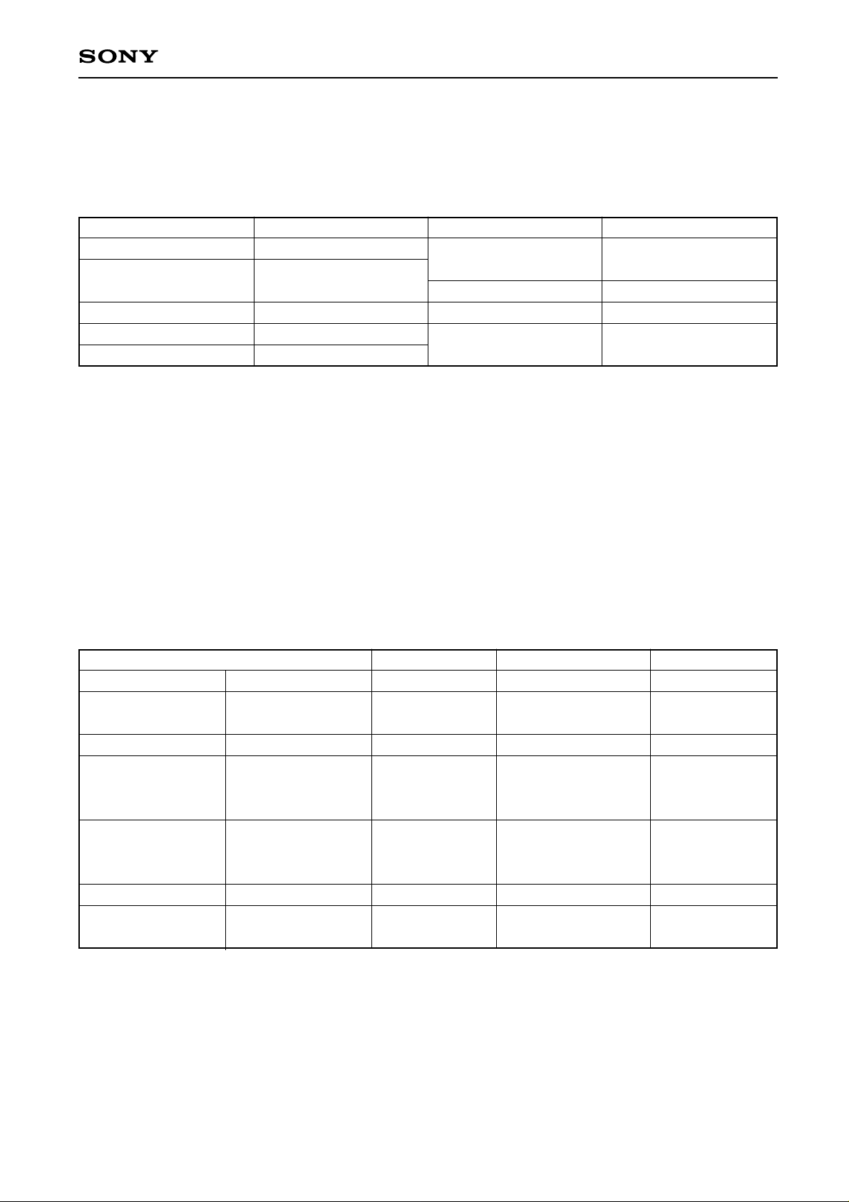
The specifications for this oscillator are outlined in table 1.
Power Supply Voltage
Output level
Output load
fout nominal frequency
fout vs. temperature
fout vs. power supply
3.3 V
0.8 Vp-p min
10 kΩ min
10 pF max
19.68 MHz
±2 ppm/°C
±0.3 ppm/V
fout vs. load
fout phase noise
Frequency control range
Control voltage range
Control voltage input
impedance
±0.2 ppm
–120 dBc/Hz min
(100 Hz offset)
235±60 Hz
+0.5 tp +2.5 V
100 kΩ min
Table 1 TCXO Oscillator requirements
9. ADC and DAC Ranges
All ADCs and DACs on the CXA3003R have internally-generated references which eliminate the need for
additional adjustment or calibration of the ADCs and DACs. All ADCs and DACs employ offset-binary
coding (Tables 2 and 3). The application of the House Keeping ADC is left up to the user. However, it
can be useful for monitoring parameters such as battery voltage and temperature. The midpoint of the
input voltage range of the House Keeping ADC is set to 1.5 V by an internal voltage reference. The input
voltage range of the ADC is 2.0 V. The gain of the ADC approximately 7.8 µ V/step.
Table 2 ADC Output Coding
Input Voltage
FM Receive ADC
Greater than positive
full-scale
Positive full-scale
99.6 % of full-scale
… …
50.2 % of full-scale
49.8 % of full-scale
… …
0.4 % of full-scale
Negative full-scale
Less than negative
full-scale
House Keeping ADC
>2.500
2.500
2.492
… …
1.504
1.496
… …
0.508
0.500
<0.500
Output Data
MSB……LSB
1111 1111
1111 1111
1111 1110
… …
1000 0000
0111 1111
… …
0000 0001
0000 0000
0000 0000
Input Voltage
CDMA Receive ADC
Greater than positive
full-scale
Positive full-scale
93.7 % of full-scale
… …
53.3 % of full-scale
46.7 % of full-scale
… …
6.7 % of full-scale
Negative full-scale
Less than negative
full-scale
Output Data
MSB…LSB
1111
1111
1110
…
1000
0111
…
0001
0000
0000
—29—
Page 30
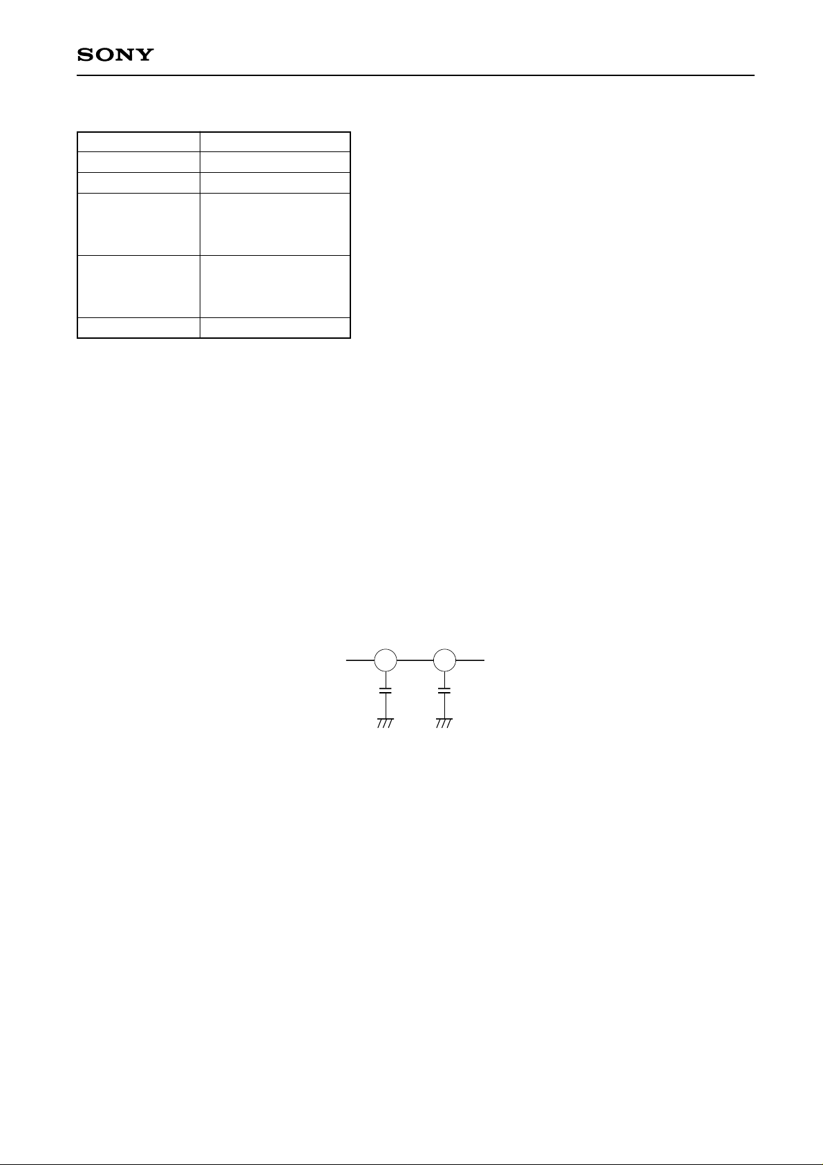
Table 3 DAC Input Coding
CXA3003R
Input Data
MSB… …LSB
1111 1111
1111 1110
… …
1000 0000
0111 1111
… …
0000 0001
0000 0000
Output Voltage
FM Transmit DAC
Positive full-scale
99.6 % of full-scale
… …
50.2 % of full-scale
49.8 % of full-scale
… …
0.4 % of full-scale
Negative full-scale
10.ADC Offset Control
The external DC voltages connected to IOFFSET and QOFFSET pins control the output of the CDMA
and FM low-pass filters to the center of the CDMA and FM ADC input range, reducing the offset to zero.
11.Receive Low Pass Filters
In CXA3003R, the receive low-pass filters remove residual IF frequency components and present
baseband I and Q components to the ADCs. The CDMA baseband signal extends from 1 kHz to 630
kHz. The FM baseband signal extends from 100 Hz to 14 kHz. The low-pass filters reject frequency
components above the passband while exhibiting a specific rate of attenuation in the transition band.
For FM Receive Filters two external bypass capacitors are required between pin 31 and GND,and
between pin 32 and GND as is shown in Fig.15.
31 32
0.01µ 0.01µ
Fig. 15 FM Receive Filter
12.Transmit Signal Path Low-Pass Filters
Low-pass filters in the transmit signal path located after the transmit DACs attenuate much of the out-ofband frequency components created by digital-to-analog conversion process. These filters are relatively
simple compared to the CDMA and FM low-pass filters found in the receive signal path. Since the gain of
the transmit signal path is low, the offset at the filter outputs are less critical. Transmit filter offsets are not
controlled as offsets are in the CDMA and FM receive paths.
—30—
Page 31

CXA3003R
13.Power Supply Considerations, Grounding, and Decoupling
The CXA3003R is targeted for use in battery operated CDMA/FM portable cellular telephones. As such,
the device has been designed to operate from a regulated 3.3 V power supply. The use of multiple
voltage regulators is recommended throughout the telephone, but the CXA3003R should be powered
from only one dedicated voltage regulator. Individual voltage regulators are usually assigned to the major
circuit subsections within the (i.e. receive RF, transmit RF, power amplifier, CXA3003R, etc.) to reduce
the possibility of signals from one subsection interfering with or distorting signals from another subsection.
The voltage regulator used in telephone for the CXA3003R should be a linear voltage regulator, not a
switching regulator. This is to keep power supply noise on the CXA3003R power inputs as low as
possible. The recommended power supply voltage range of the CXA3003R is from 3.13 to 3.47 V (3.3±5
%). It is recommended that a ±2 % accurate regulator be used so that the proper output voltage can be
maintained over the temperature range of the telephone and over the power supply current range of the
CXA3003R.
Power supply decoupling around the CXA3003R is done with 0.01 µF ceramic chip capacitors on each
VDD pin. The capacitors are located as close to the pins as possible to minimize series inductance in the
connection to the pin. The use of additional 0.001 µF decoupling capacitors in parallel with the 0.01 µF
capacitors is recommended to further reduce high frequency noise on the power supply inputs to the
CXA3003R.
Although the CXA3003R has both analog and digital circuits and separate digital power and ground pins
a single ground plane is recommended. The ground plane must overlap the footprint of the CXA3003R
as much as possible. ALL CXA3003R ground pins must be connected to the same analog ground plane.
—31—
Page 32
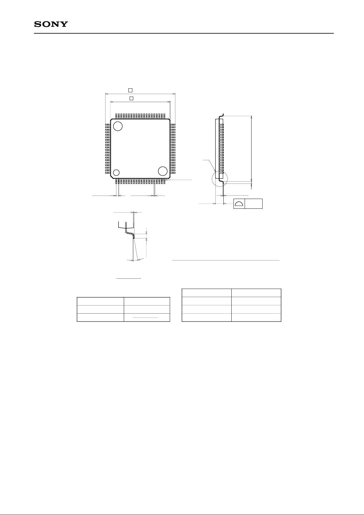
Package Outline Unit : mm
80PIN LQFP (PLASTIC)
14.0 ± 0.2
∗ 12.0 ± 0.1
61
80
0.5 ± 0.08
SONY CODE
EIAJ CODE
JEDEC CODE
60
1
0.1 ± 0.1
0° to 10°
DETAIL A
+ 0.08
0.18 – 0.03
0.5 ± 0.2
LQFP-80P-L01
∗QFP080-P-1212-A
41
40
A
21
(0.22)
20
+ 0.2
1.5 – 0.1
NOTE: Dimension “∗” does not include mold protrusion.
0.127 – 0.02
(13.0)
0.5 ± 0.2
+ 0.05
0.1
PACKAGE STRUCTURE
PACKAGE MATERIAL
LEAD TREATMENT
LEAD MATERIAL
PACKAGE WEIGHT
EPOXY / PHENOL RESIN
SOLDER PLATING
42 ALLOY
0.5g
—32—
 Loading...