

Page 1

—1—
E97705A85-TE
Sony reserves the right to change products and specifications without prior notice. This information does not convey any license by
any implication or otherwise under any patents or other right. Application circuits shown, if any, are typical examples illustrating the
operation of the devices. Sony cannot assume responsibility for any problems arising out of the use of these circuits.
Absolute Maximum Ratings (Ta=25 °C)
• Supply voltage VCC –0.3 to +5.5 V
• Storage temperature Tstg –55 to +150 °C
• Allowable power dissipation
PD 625 mW
(when mounted on a printed circuit board)
Operating Conditions
• Supply voltage VCC 4.75 to 5.30 V
• Operating temperature Topr –20 to +75 °C
Description
The CXA3125N is a TV tuner IC which integrates
local oscillator and mixer circuits for VHF band, local
oscillator and mixer circuits for UHF band, and an IF
amplifier onto a single chip. This IC adopts a 16-pin
SSOP package and is suitable for miniaturizing
voltage synthesizer tuner.
Features
• Low noise figure
• Superior cross modulation
• Low power consumption (5 V, 43 mA typ.)
• IF output can be selected from symmetrical or
asymmetrical
• SSOP 16-pin package
Applications
• TV tuners
• VCR tuners
• CATV tuners
Structure
Bipolar silicon monolithic IC
All Band TV Tuner IC (VHF-CATV-UHF)
16 pin SSOP (Plastic)
CXA3125N
For the availability of this product, please contact the sales office.
Page 2

—2—
CXA3125N
Block Diagram and Pin Configuration
CXA3125N
OUTPUT
Buffer
UHFOSC
IF AMP
UHFMIXVHFMIX
VHFOSC
IFout1
IFout2
UOSC2
BSW
UOSC1
VOSC2
IFSW
VOSC1
V
CC
MIXout1
MIXout2
GND
VHFin1
VHFin2
UHFin1
UHFin2
V.REG
Bias
1 2 6 7 83 4 5
15 14 12 11 10 916 13
Page 3

—3—
CXA3125N
Pin Description and Equivalent Circuit
Pin
Symbol
Typical pin
Equivalent circuit Description
No. voltage (V)
1
2
3
4
5
6
7
8
9
11
VCC
MIXout1
MIXout2
GND
VHFin1
VHFin2
UHFin1
UHFin2
VOSC1
VOSC2
5.0
During VHF
reception 4.4
During UHF
reception 4.3
4.4
4.3
0
2.4
0
2.4
0
0
2.4
0
2.4
3.1
3.2
4.0
5.0
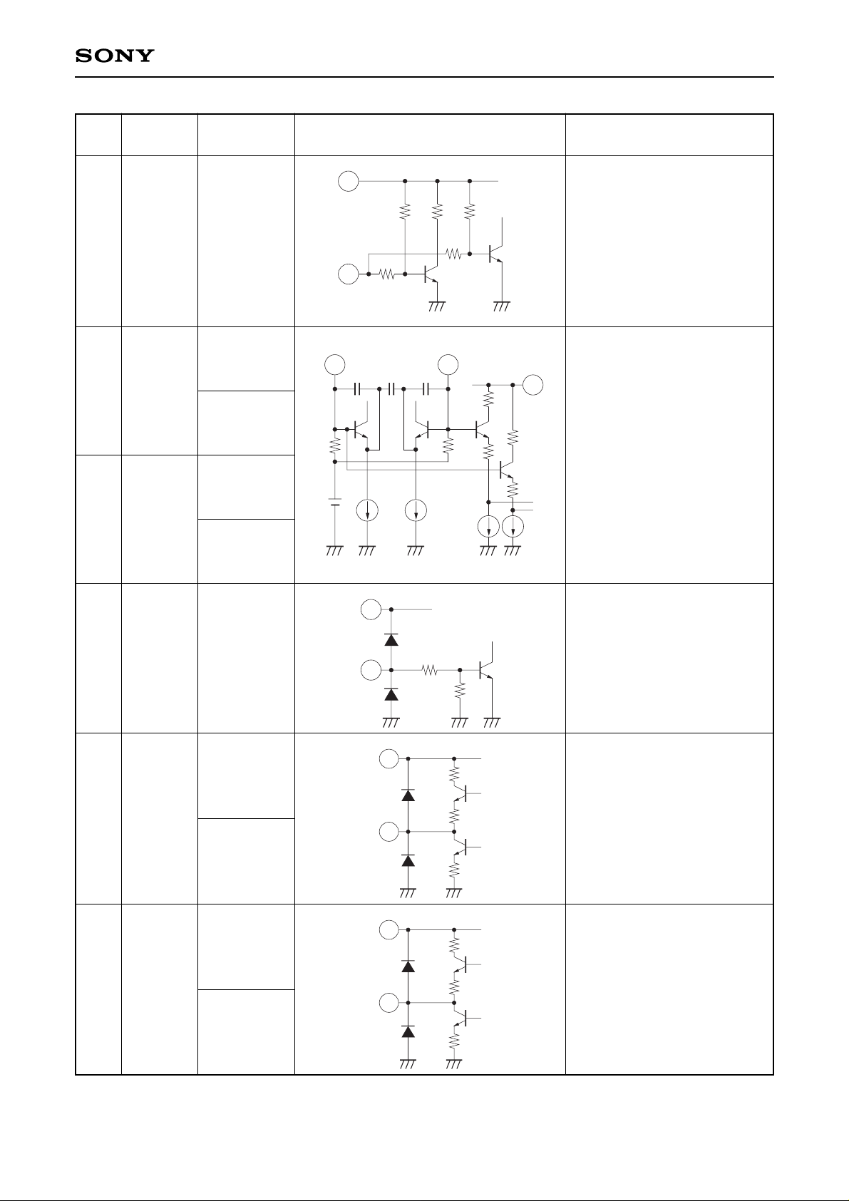
Power supply.
Mixer outputs and IF amplifier
inputs. These pins are output
with open collector, and they
must be connected to power
supply via load.
GND.
VHF inputs.
Normally a capacitor is
connected at Pin 5 to GND and
Pin 6 is used for input.
UHF inputs. Symmetrical input
to Pins 7 and 8 or a capacitor
is connected at Pin 8 to GND
and Pin 7 is used for input.
External resonance circuit
connection for VHF oscillators.
2 3
6
3k3k
5
8
3k3k
7
11
330
3k
8p
15p
3k
9
50
1
VCC
Page 4
—4—
CXA3125N
Pin
Symbol
Typical pin
Equivalent circuit Description
No. voltage (V)
10
12
14
13
15
16
IFSW
UOSC1
UOSC2
BSW
IFout2
IFout1
0.8
(when open)
3.2
3.0
3.2
3.0
—
During
symmetrical
output 3.0
During
asymmetrical
output 4.3
During
symmetrical
output 3.0
During
asymmetrical
output 2.5
Symmetrical/asymmetrical
selection of IF output.
Asymmetrical output is selected
for open state; symmetrical
output, for connecting to GND.
When used as an asymmetrical
output, connect to GND with a
capacitor.
External resonance circuit
connection for UHF oscillators.
Band switching.
UHF operation when 3 V or
more voltage is applied
externally, and VHF operation
when 0.5 V or less voltage is
applied.
IF outputs during symmetrical
output. The reverse phase
signal to Pin 16 is output
during symmetrical output.
When asymmetrical output is
selected, the signal is not
output.
IF outputs.
3k 3k
1
VCC
1214
VCC
1
13
22k
32k
40k
VCC
1
30k
10
400
20k
400
30k
VCC
1
15
15
VCC
1
16
15
Page 5

—5—
CXA3125N
Electrical Characteristics See the Electrical Characteristics Measurement Circuits 1 and 2.
(Ta=25 °C, VCC=5 V)
Item
Circuit current
Conversion gain
∗1
Noise figure
∗1, ∗2
1 % cross
modulation
∗1
∗3
Maximum
output power
Switch ON drift
∗4
+B drift
∗5
Band switch
voltage
Symbol
ICCVU
ICCVB
ICCUU
ICCUB
CG1U
CG2U
CG3U
CG4U
CG1B
CG2B
CG3B
CG4B
NF1
NF2
NF3
NF4
CM1
CM2
CM3
CM4
Pomax
(sat)
∆fsw1
∆fsw2
∆fsw3
∆fsw4
∆fst1
∆fst2
∆fst3
∆fst4
VSWV
VSWU
Measurement conditions
VHF operation asymmetrical output no input signal
VHF operation symmetrical output no input signal
UHF operation asymmetrical output no input signal
UHF operation symmetrical output no input signal
VHF operation fRF=55 MHz asymmetrical output
VHF operation fRF=360 MHz asymmetrical output
UHF operation fRF=360 MHz asymmetrical output
UHF operation fRF=800 MHz asymmetrical output
VHF operation fRF=55 MHz symmetrical output
∗6
VHF operation fRF=360 MHz symmetrical output
∗6
UHF operation fRF=360 MHz symmetrical output
∗6
UHF operation fRF=800 MHz symmetrical output
∗6
VHF operation fRF=55 MHz asymmetrical output
VHF operation fRF=360 MHz asymmetrical output
UHF operation fRF=360 MHz asymmetrical output
UHF operation fRF=800 MHz asymmetrical output
VHF operation fD=55 MHz fUD=±12 MHz
asymmetrical output
VHF operation fD=360 MHz fUD=±12 MHz
asymmetrical output
UHF operation fD=360 MHz fUD=±12 MHz
asymmetrical output
UHF operation fD=800 MHz fUD=±12 MHz
asymmetrical output
50 Ω load, asymmetrical output
VHF operation fOSC=100 MHz
VHF operation fOSC=405 MHz
UHF operation fOSC=405 MHz
UHF operation fOSC=845 MHz
VHF operation fOSC=100 MHz
VHF operation fOSC=405 MHz
UHF operation fOSC=405 MHz
UHF operation fOSC=845 MHz
VHF operation
UHF operation
Min. Typ. Max. Unit
32 43 52 mA
35 46 55 mA
33 44 53 mA
36 47 56 mA
22 25 28 dB
22 25 28 dB
27 30 33 dB
27 30 33 dB
26 29 32 dB
26 29 32 dB
31 34 37 dB
31 34 37 dB
11 15 dB
11 15 dB
9 12 dB
9.5 12.5 dB
96 100 dBµ
96 100 dBµ
90 94 dBµ
90 94 dBµ
+10 dBm
±300 kHz
±400 kHz
±400 kHz
±400 kHz
±200 kHz
±250 kHz
±250 kHz
±250 kHz
0 0.5 V
3 5.5 V
∗1
Input level –40 dBm, Value measured with untuned input.
∗2
Noise figure is the NF meter direct-reading value (DSB measurement).
∗3
Value with a desired reception signal input level of –30 dBm, an interference signal of 100 kHz at ±12 MHz
: 30 % AM, and an interference signal level where S/I=46 dB measured with a spectrum analyzer.
∗4
Frequency variation from 3 seconds to 3 minutes after switch ON.
∗5
Frequency variation when VCC=5 V ±5 % variation.
∗6
Value which is measured as 410 Ω load impedance and compensated loss by 180 Ω resistor connected to
Pins 15 and 16.
Page 6

—6—
CXA3125N
Electrical Characteristics Measurement Circuit 1 (asymmetrical output)
IFout1
IFout2
UOSC2
BSW
UOSC1
VOSC2
IFSW
VOSC1
V
CC
MIXout1
MIXout2
GND
VHFin1
VHFin2
UHFin1
UHFin2
CXA3125N
IF OUT
1n
1n
56p
10k
56p
47k
47k
8p
1T363
2.6φ2.5t
0.5p
0.5p
1T363
47k
BAND SW
ON : UHF
OFF : VHF
+5V
1p (UK)
47k
47k
1T362
16p
20
0.5p (UK)
1T363
47k
68p (RH)
3.2φ
2.5t
1n
47k
51
3.2φ
6.5t
51
VL
VH
1n
1n
1.2k
1n3.3µ
Vt
+5V
2k
L1
56p 56p
100
1n
1n
3.3µ
+5V
1n 1n
1n 1n
VHF IN UHF IN
1 2 6 7 83 4 5
15 14 12 11 10
9
16 13
1n
L1 is a pentagonal coil 4.5 t/4.5 t
L without indication is an air-core coil of 0.5 mm diameter.
These components value are the setting for USA frequency variation range.
Page 7

—7—
CXA3125N
Electrical Characteristics Measurement Circuit 2 (symmetrical output)
IFout1
IFout2
UOSC2
BSW
UOSC1
VOSC2
IFSW
VOSC1
V
CC
MIXout1
MIXout2
GND
VHFin1
VHFin2
UHFin1
UHFin2
CXA3125N
IF OUT
1n
1n
56p
10k
56p
47k
47k
8p
1T363
2.6φ2.5t
0.5p
0.5p
1T363
47k
BAND SW
ON : UHF
OFF : VHF
+5V
1p (UK)
47k
47k
1T362
16p
20
0.5p (UK)
1T363
47k
68p (RH)
3.2φ
2.5t
1n
47k
51
3.2φ
6.5t
51
VL
VH
1n
1n
1.2k
1n3.3µ
Vt
+5V
2k
L1
56p 56p
100
1n
1n
3.3µ
+5V
1n 1n
1n 1n
VHF IN UHF IN
1 2 6 7 83 4 5
1n
180
180
15 14 12 11 10
9
16 13
L1 is a pentagonal coil 4.5 t/4.5 t
L without indication is an air-core coil of 0.5 mm diameter.
These components value are the setting for USA frequency variation range.
Page 8

—8—
CXA3125N
Description of Operation
(See the Electrical Characteristics Measurement Circuit.)
VHF oscillator circuit
This circuit is a differential amplifier type oscillator circuit. Pin 11 is the output and Pin 9 is the input.
Oscillation is performed by connecting an LC resonance circuit including a varicap to Pin 11 via coupled
capacitance, inputting to Pin 9 with feedback capacitance, and applying positive feedback.
Note that if the capacitance across Pins 9 and 11 is too large, positive feedback may be applied via a
parasitic capacitance causing undesired stray oscillation.
VHF mixer circuit
The mixer circuit employs a double symmetrical mixer with little local oscillation signal leakage. The RF
signal is input to Pins 6 and 7. During normal use, the RF signal is input to one pin while the other pin is
connected to GND. The RF signal is converted to IF frequency by the signal supplied from the oscillator and
then output to Pins 2 and 3. Pins 2 and 3 are open collectors, so power must be supplied externally.
Connect to VCC through L which configures external filter or resistor. The electric potential of Pins 2 and 3 at
this time must be DC 4.0 V or more.
UHF oscillator circuit
This oscillator circuit is designed so that two collector ground type Colpitts oscillators perform differential
oscillation operation via an LC resonance circuit including a varicap. Feedback capacitance is built into IC,
and an LC resonance circuit including a varicap is connected between Pins 12 and 14 via coupled
capacitance.
UHF mixer circuit
This circuit employs a double symmetrical mixer like the VHF mixer circuit. The RF signal is input to Pins 7
and 8. There is a symmetrical input at the differential from both edges of the secondary coil of the pre-stage
double-tuned circuits, or an asymmetrical input to Pin 7 with a capacitor connected at Pin 8 to GND.
Otherwise, the conditions and usage are the same as those for the VHF mixer circuit.
IF amplifier circuit
The signals frequency converted by the mixer are output from Pins 2 and 3, and at the same time are AC
coupled inside the IC and input to the IF amplifier. Single-tuned filters are connected to Pins 2 and 3 in order
to improve the interference characteristics of the IF amplifier.
The signal amplified by the IF amplifier is output with symmetrical or asymmetrical output format. Selecting
symmetrical or asymmetrical is performed at Pin 10. Asymmetrical output when Pin 10 is for open state;
symmetrical output when connected to GND. During symmetrical output, SAW filter direct connection is
possible and during asymmetrical output, output stage drive capability is increased to drive 75 Ω load.
During asymmetrical output, output is performed from Pin 16, and during symmetrical output, output is
performed from Pins 15 and 16. The output impedance is approximately 35 Ω for symmetrical output; 30 Ω
for asymmetrical output. When asymmetrical output is selected, connect Pin 10 to GND through capacitor.
U/V switch circuit
UHF operation is chosen by applying voltage of 3 V or more to Pin 13 VHF operation for 0 V or open.
Page 9

—9—
CXA3125N
Notes on Operation
1. Care should be taken for grounding, etc. when placing external parts as high operating frequencies are
present.
2. The GND pattern also serves as heat dissipation pins, care should be taken to prevent heat problems.
3. Care should also be taken to prevent electrostatic damage because of using high frequency process.
Page 10

—10—
CXA3125N
Example of Representative Characteristics
100
DRIFT [kHz]
Supply voltage vs. Circuit current
(for asymmetrical output)
I
CC
- Circuit current [mA]
VCC - Supply voltage [V]
Reception frequency vs. Conversion gain
(for asymmetrical output)
CG - Conversion gain [dB]
Reception frequency [MHz]
Reception frequency vs. Noise figure
(untuned input, for asymmetrical output, DSB display)
NF - Noise figure [dB]
Reception frequency [MHz]
15
10
5
0
Reception frequency vs. +B drift
Reception frequency [MHz]
Reception frequency vs. Next adjacent cross modulation
(untuned input, for asymmetrical output)
CM - Cross modulation [dBµ]
Reception frequency [MHz]
120
100
80
60
40
20
0 200 300 400 500 600 700 800 900100
I/O characteristics (untuned input, for asymmetrical output)
IF output level [dBm]
RF input level [dBm]
54
44
34
4 5 6
: VHF
: UHF
VHF
UHF
fIF=45MHz
40
30
25
20
15
10
5
0
100 200 300 400 500 600 700 800 900
VHF
UHF
fIF=45MHz
200 300 400 500 600 700 800 900
400
200
0
–200
–400
0 200 400 600 800 1000
f
IF=45MHz 100kHz 30% AM
fUD=fD+12MHz
fUD=fD–12MHz
20
0
–20
–40
–60
f
RF=100MHz (VHF)
fRF=450MHz (UHF)
fIF is both f=45 MHz.
–60 –40 –20 0
Page 11

—11—
CXA3125N
50MHz
0
50
j100
j50
j25
–j50
–j25 –j100
1000p
S11
VHFin1
VHFin2
350MHz
5 6
0
50
j100
j50
j25
–j50
–j25 –j100
1000p
S11
UHFin1
UHFin2
350MHz
7 8
800MHz
VHF Input Impedance
UHF Input Impedance
Page 12

—12—
CXA3125N
0
50
j100
j50
j25
–j50
–j25 –j100
45MHz
38MHz
0
50
j100
j50
j25
–j50
–j25 –j100
45MHz
38MHz
IF Output Impedance (symmetrical output)
IF Output Impedance (asymmetrical output)
Page 13

16PIN SSOP (PLASTIC)
SONY CODE
EIAJ CODE
JEDEC CODE
PACKAGE STRUCTURE
PACKAGE MATERIAL
LEAD TREATMENT
LEAD MATERIAL
PACKAGE MASS
EPOXY RESIN
SOLDER / PALLADIUM
42/COPPER ALLOY
0.1g
SSOP-16P-L01
SSOP016-P-0044
∗5.0 ± 0.1
0.65
0.22 – 0.05
+ 0.1
8
1
9
16
∗4.4 ± 0.1
6.4 ± 0.2
0.1 ± 0.1
0.5 ± 0.2
0° to 10°
0.15 – 0.02
+ 0.05
1.25 – 0.1
+ 0.2
A
DETAIL A
0.1
PLATING
NOTE: Dimension “∗” does not include mold protrusion.
0.13
M
Package Outline Unit : mm
CXA3125N
—13—
 Loading...