


CPX8000
Table of contents
 Loading...
CPX8000 Series CPX8216/CPX8216T
®
CompactPCI
System
Reference Manual
CPX8216A/RM4
August 2002 Edition

© Copyright 2002 Motorola Inc.
All rights reserved.
Printed in the United States of America.
Motorola® and the Motorola symbol are registered trademarks of Motorola, Inc.
PowerPC® and the PowerPC logo are registered trade mark s of International Business
Machines Corporation (IBM) and are used by Motorola, Inc. under license from IBM.
CompactPCI® is a registered trademark o f the PC I In dustrial Computer Manufacturer’s
Group (PICMG).
All other product or service names mentioned in this doc ument are trademarks or registered
trademarks of their respective holders.

Safety Summary
Warning
The followi ng gen eral safety precaut io ns mus t be observed during all ph ases of oper ation, service, an d repa ir of
this equipment. Failure to comply with these precautions or with specific warnings elsewhere in this manual
could result in personal injury or damage to the equipment.
The safety precautions listed below represent warnings of certain dangers of which Motorola is aware. You, as
the user of the product, should follow these warnings and all other safety precautions necessary for the safe
operation of the equipment in your operating environment.
Ground the Instrument.
T o minimi ze shock haz ard, the equi pment chassis and enclosure must be connec ted to an electr ical ground . If the
equipment is supp lied with a three-co nduct or AC power cable, th e powe r cabl e mus t be plu gged int o an approv ed
three-con tact e lectrical outlet, with the groundin g wir e (green/yellow) r eliab ly co nnected to an electrical ground
(safety ground) at the power outlet. The power jack and mating plug of the power cable meet International
Electrotechnical Commission (IEC) safety standards and local electrical regulatory codes.
Do Not Operate in an Explosive Atmosphere.
Do not operate the equipm ent in a ny explosive atm osp here such as in the presence of flam mabl e g ases or fumes.
Operation of any electrical equipment in such an environment could result in an explosion and cause injury or
damage.
Keep Away From Live Circuits Inside the Equipment.
Operating personnel must not remove equipment covers. Only Factory Authorized Service Personnel or other
qualified service personnel may remove equipment covers for internal subassembly or component replacement
or any inte rnal adjus tment. Se rvice pe rsonnel s houl d not repl ace comp onents w ith power cab le co nnected . Under
certain conditions, dangerous voltages may exist even with the power cable removed. To avoid injuries, such
personnel should always disconnect power and discharge circuits before touching components.
Use Caution When Exposing or Handling a CRT.
Breakage of a Cathode-Ray Tube (CRT) causes a high-velocity scattering of glass fragments (implosion). To
prevent CRT implo sion , do not ha ndl e the CRT and avo id roug h handling or jarrin g of t he equ ipm ent . Ha ndling
of a CRT should be done only by qualified service personnel using approved safety mask and gloves.
Do Not Substitute Parts or Modify Equipment.
Do not install substitute parts or perform any unauthorized modification of the equipment. Contact your local
Motorola representative for service and repair to ensure that all safety features are maintained.
Observe Warnings in Manual.
Warnings, such as the example below, precede potentially dangerous procedures throughout this manual.
Instructions contained in the warnings must be followed. You should also employ all other safety precautions
which you deem necessary for the operation of the equipment in your operating environment.
Warnin g
To prevent serious injury or death from dangerous voltages, use extreme
caution when handling, testing, and adjusting this equipment and its
components.

Flammability
!
Warning
All Motorola PWBs (printed wiring boards) are manufactured with a flammability rating
of 94V-0 by UL-recognized manufac turers.
CE Notice (European Community)
Warnin g
Motorola Computer Group p roducts with t he CE marking comply wi th the EMC Dir ective
(89/336/EEC). Compliance with this dir ective implies conformity to the following
European Norms:
EN55022 “Limits and Methods of Measurement of Radio Interference Characteristics
of Information Technology Equipment”; this product tested to Equipment Class A
EN55024 “Information technol ogy equipment—Immunity characteristics—Limits and
methods of measurement”
This product also fulfill s EN60950 (pr oduct safety) which is essentially the requir ement fo r
the Low Voltage Directive (73/23/EEC).
AC configurations of this system also mee t the req uirements of the following European
standards:
EN61000-3-2 “Limits of Harmonic Current Emissions (equipment input current ≤ 16
A per phase)”
This is a Class A product. In a domestic environment, this product may
cause radio interference, in which case the user may be required to take
adequate measures.
EN61000-3-3 “Limits of Voltage Fluctuations and Flicker in Low-Voltage Supply
Systems for Equipment with Rated Current ≤ 16 A”
In accordance with European Community directives, a “Declaration of Conformit y” has
been made and is available on request. Please contac t your sales representative.
This product is not a workstation per the Europe an Ergonomic Standard.
Kein Bildschirmarbeitsplatz nach dem Europäischen Ergonomie Standard.

FCC Class A
!
Caution
This equipment ha s been tested and found to comply with the limits for a Class A digital
device, pursuant to Part 15 of the FCC Rules. These lim its are designed to provide
reasonable protec tion against harmful interferen ce when the equipment is operated in a
commercial environm ent. Thi s equipment g enerates , uses, and can rad iate radio f requency
energy and, if not ins talle d and used in accordance with the instr uction manual, may cause
harmful interference to radio communications. Operati on of this equipment in a residential
area is likely to cause ha rmful interference in which case the use r will be required to c orrect
the interference at his own expense.
Changes or modifications no t expre ssly approve d by Motor ola Computer Group could voi d
the user’s author ity to operate the equipment.
Use only shielded cables when connecting peripherals to assure that appropriate radio
frequency emissions co mpli ance is maintained.
EMI Caution
Caution
This equipment generates, uses and can radiate electromagnetic energy. It
may cause or be susceptible to electromagnetic interference (EMI) if not
installed and used with adequ at e EMI protection.
Notice
While reasonable ef forts have been made to assure the accuracy of this document,
Motorola, Inc. assumes no liabil ity re sult ing from any o missions i n thi s document, or f rom
the use of the information obtained therein. Motorola reserves the right to revise this
document and to make ch ang es from time to time in the content hereof without obligation
of Motorola to notify any person of such revision or changes.
Electronic versi ons of this material may be read online, downloaded for personal use, or
referenced in another document as a UR L to the Motorola Compute r Group Web site. The
text itself may not be published commercially in prin t or electr onic form, e dited, transla ted,
or otherwise altered without the permission of Motorola, Inc.
It is possible that this publication may con tain reference to or information about Motorola
products (mach ines and pro grams), p rogramming, or s ervi ces tha t ar e not avail able in your

country. Such references or inform at ion must not be construed to mean that Motorola
intends to announce such Motorola produc ts, programming, or services in your country.
Limited and Restricted Rights Legend
If the documentation containe d here in is supplied, directly or indirectly, to the U.S.
Government, the following notice shall apply unless otherwise agreed to in writing by
Motoro la , Inc.
Use, duplication, or disclosure by the Government is subject to restrictions as set forth in
subparagraph (b)(3) of the Rights in Technical Data clause at DFARS 252.227-7013 (Nov.
1995) and of the Rights in Nonc ommercial Compute r Software a nd Documenta tion clause
at DF ARS 252.227-7014 (Jun. 1995).
Motoro la , Inc.
Computer Group
2900 South Diablo Way
T empe, Arizona 85282

About t his Manual
Summary of Changes ................................................................................................xix
Systems Supported ........................... .................... ............................... .................... ..xxi
Overvie w ............ .............. ............... ...................... ...................... ..................... ........xxi i
Comments and Suggestions ................................................................................ .....xxii
Conventions Used in This Manual ......................................................................... xxiii
CHAPTER 1 System Architecture
PICMG Compliance ................................................................................................. 1-1
System D o m a in s ............. .......... ......... ................. .......... .......... ......... .......... ............... 1-1
System Layout .... ......... ................. .......... .......... .......... ................. ......... .......... .......... 1 -2
CPX821 6 ....... .......... .......... ....... .......... ......... .......... .......... ....... .......... ......... ........ 1 -2
CPX8216T (H.110) ........................................................................................... 1-4
Bus Access and Control ........................................................................................... 1-4
The Hot Swap Controlle r/Bridge (HSC) Module ............................... .................... .1-5
Hot Swap Co n t ro l le r . .. ... .......... ......... .......... ................. .......... ......... .......... ............... 1-6
System Processor Configurations ............................................................................ 1-7
The Simplex Configuration ............................................................................... 1-7
The Active/Passive Configuration .................................................................... 1-8
The Active/Active or Load-Sharing Configuration .......................................... 1-9
I/O Configurations ................................................................................................. 1-10
Periphe rals ..... .......... ....... .......... ......... .......... .......... ....... .......... ......... .......... .......... ... 1-10
Power/Fan Modules ........................................................................................ 1-10
Drive Modules .................................................................................................1-11
CPU Complex Architecture ................................................................................... 1-12
The CPU Module ....... .......... .................... ......................................... .......... .... 1-12
Switching Service to the Passive CPU ............................................................ 1-13
Chassis ID for CPX8216T ..................................................................................... 1-13
Alarms and LEDs ................................................................................................... 1-13
H.110 Telephony Bus ............................................................................................. 1-14
Board Insertion and Extraction Features ................................................................ 1-14
Staged Pin s .. ......... ................. .......... .......... .......... ................. ......... .......... ........ 1 -15
BD_SEL# ............. ...................... ...................... ............... ...................... .......... 1-15
ENUM# ......... .......... .......... ......... ........ ......... .......... .......... ......... ........ ......... ...... 1-15
Contents
vii

Hot Swap Control Status Register (CSR) ........................................................ 1-16
The Hot Swap Process ............................................................................................1-16
Physical Connection Process ........................................................................... 1-17
Hardware Connection Process ......................................................................... 1-17
Software Connection Process ..........................................................................1-18
Software Disconnect ion P rocess .................... .. ............ ........................ ...........1-18
Typical Insertion and Extraction Processes ..................................................... 1-19
Devic e D r iv er s ............ .......... ......... ................. .......... .......... ......... .......... ................. 1- 1 9
CHAPTER 2 CPU Modules
Overview .................................................................................................................. 2-1
CPX75 0 H A .......... ......... .......... .......... ................. ......... .......... .......... ................. ......... 2- 1
Connectors and Jumper Settings ....................................................................... 2-4
Backplane Connectors (P5, P4, P3, P2, P1) ................... .......... ..................2-4
Front USB Connectors (J1 7 and J 18) .................... .................... .................2-4
10BaseT/100BaseTx Connector (J8) .........................................................2-4
COM1 Connector (J15) ................ ..............................................................2-5
Debug Connector (J 19) ..............................................................................2-6
DRAM M ez zanine C onn ector (J1 0) .......... .......... ......... .......... ................. 2- 1 0
EIDE Compact FLASH Connector (J9) ...................................................2-14
Flash Bank Selection (J6) ......................................................................... 2-15
CPV5350 ................................................................................................................2-16
Conn ectors ...... ....... ........ ....... ..... ....... ....... ........ ....... ..... ....... ....... ........ ....... ..... ..2-18
Transition Module ......................... ............................... .................... ...............2-19
DRAM Memory Configuration ....................................................................... 2-20
Keyboard/Mouse PS2 Connector ....................................................................2-20
Ethe rne t C on n e ctors ...... ................. ......... .......... .......... ......... ................. .......... 2-2 1
Universal Serial Bus (US B) Conne ctor .......... ............ ........................ ............ .2-21
Serial Port Connectors .....................................................................................2-22
Video Connector .............................................................................................. 2-22
CHAPTER 3 CPX8540 Carrier Card
Overview .................................................................................................................. 3-1
CPX8540 Carrier Car d .............. ........ ................... ........ ................... .........................3-1
Connector Pinouts ..................................................................................................... 3-4
viii

CHAPTER 4 PMC Modules
Overvie w ............ .............. ............... ...................... ...................... ..................... ........ 4-1
SCSI-2 Controller PMC ........................................................................................... 4-1
Switc h Se tt in g s ........ .......... ......... .......... ................. .......... ......... .......... .......... ..... 4-3
Conne ct or Pin A ss i g nm en ts ............ .......... .......... ......... ................. .......... .......... 4-4
CHAPTER 5 Transition/Bridge Modules
Overvie w ............ .............. ............... ...................... ...................... ..................... ........ 5-1
CPX750 H ATM Transitio n M o dule . .. ................. .......... .......... ......... ................. ........ 5-1
Serial Ports 3 and 4 Default Configuration ....................................................... 5-2
Serial Port Interface Jumper (J8 and J9) ........................................................... 5-4
Connectors ........................................................................................................ 5-4
Backplane Connectors (J3/J4/J5) ............................................................... 5-4
Asynchronous Serial Port Connectors (J10 and J11) ................................. 5-6
Asynchronous/S ynchronous Serial Port Connectors (J6 and J24) ............. 5-7
Parallel I/O Port Connector (J7) ................................................................ 5-9
Keyboard/Mouse Conne ctor (J16) .................. ............ ............ ................. 5-10
USB Connectors (J19 and J18) ................................................................ 5-10
EIDE Connector (J15) ............................................................................. 5-11
Floppy Port Connector (J 17) .............................................. ........... ........... 5-12
+5Vdc Power Connector (J14) ................................................................ 5-12
Speaker Output Connector (J13) ........................ ........................ ............ ..5-13
PMC I/O Connectors ............................................................................... 5-14
Installing the Serial Interface Modules ........................................................... 5-16
Port Con f ig u ration Dia g r am s .......... ... ......... .......... .......... ......... ................. ...... 5-18
COM1 and COM2 Asynchronous Serial Ports ........................................ 5-18
Asynchronous/Synchronous Serial Ports ................................................. 5-20
CPV535 0 TM80 Transi tion Modu l e ....... ... .. .......... ......... ................. .......... .......... ... 5-29
Connectors ...................................................................................................... 5-31
Keyboard/Mouse PS2 Connector ............................................................. 5-32
Ethernet Connectors ...................................... ............ ........................ ....... 5-33
Serial Port Connectors ............................................................................. 5-33
Video Connector ...................................................................................... 5-34
Parallel Port Connector (J20) ................................................................... 5-35
EIDE Headers (J5) ................................................................................... 5-36
Floppy Header (J9) .............. ........................... .........................................5-38
Keyboard/Mouse/ Power LED Header (J6) ................. ............. ................5-40
USB Headers (J12 and J19) ..................................................................... 5-41
SM Bus and LM78 Header (J1) ............................................................... 5-42
Fan Tachometer Headers (J3 and J4) ....................................................... 5-43
ix

Indicator LED/Miscellaneous Header (J2) ............................................... 5-43
CHAPTER 6 Subassembly Reference
Chapt er Over vie w .. ..... ..... ..... .... ... ..... ..... .... ..... ... ..... .... ..... ..... ... .... ..... ..... ..... .. ..... ..... .. 6-1
Parts of the System ................................................................................................... 6-2
CompactPCI Card Cage Reference .......................................................................... 6-4
Backplane Reference ................................................................................................ 6-5
Power Supply Connectors (PS1, PS2, PS3) ......... ............ ........................................6-6
H.110 Power Connector (CPX8216T Only) .............................................................6-7
Alarm Interface Connect or (ALARM) ..... ............ ............ ........................................6-8
Floppy Drive Connectors (FDA, FDB) ....................................................................6-8
IDE Drive Connectors (IDEA and IDEB) ........ ............ ............ .. ............ ..................6-9
Peripheral Power Connectors (PWR1, PWR2, PWR3, PWR4) .............................6-10
Peripheral Signal Connectors (SIG1, S IG2, SIG3, SIG4) ......................................6-11
CompactPCI Connectors (P1, P2, P3, P4, P5)—CPX8216 Sta ndard Backplane ..6-11
Primary (Front) Side I/O Connectors (Slots 1-6 and 11-16) ...........................6-11
Primary (Front) Side CPU Slot Connectors (7 and 9) .....................................6-17
Secondary (Rear) Side I/O Connectors .......... ........................ ............ ............ .6-26
CPU Transition Module Connectors
(Transition Slots 7 and 9) ....................................................................................... 6-27
Hot Swap Controller/Bridge Connectors (Transition Slots 8 and 10) ....................6-29
H.110 Bus Conne ctors—CPX8216T System Only ............................................. ...6-37
Primary (Front) Side I/O Connectors ....................................................................6-38
Primary (Front) Side (Slots 1-6 and 11-16) .................................................... 6-38
Primary (Front) Side CPU Connectors ............................................................ 6-40
Primary (Front) Side HSC Connectors ............................................................ 6-40
Secondary (Rear) Side I/O Connectors ............................. ............ .. ............ .. .........6-50
Secondary (Rear) Side CPU Transition Module Connectors ............... .. ................6-50
Alarm Display Panel ............................................................................................... 6-51
Alarm Display Panel Interface Connector (J 4) ............... .. ............ ..........................6-53
Remote Alarm Connector (J1) ................................................................................6-53
Power Distribution Panel ........................................................................................6-54
AC Power Distribution Panel (CPX8216) ....................................................... 6-54
Dual Input DC Power Distribution Panel (CPX8216) ........ .. ..........................6-55
Dual Breaker DC Power Distribution Panel (CPX8216) ................................6-55
H.110 DC Power Distribution Panel (CPX8216T) ......................................... 6-56
Power Supplies ............... .. ............ .. ............ ............................................................6-58
x

APPENDIX A Specifications
Environ m e n tal Characterist i cs ........ .......... ......... ................. .......... .......... ......... ........A -1
Power Supply Electrical Specifications ...................................................................A-2
APPENDIX B Related Documentation
Motorola Comput er Group Documents ....................................... ............................B-1
Related Specifications ..............................................................................................B-2
URLs ........................................................................................................................B-4
xi

List of Figures
Figure 1-1. CPX8216 Domains ............................................................................... 1-2
Figure 1-2. CPX8216 Standard System Layout ...................................................... 1-3
Figure 1-3. CPX8216T H.110 System Layout ........................................................ 1-4
Figure 1-4. CPX8216 I/O Bus Connectivi ty ....... ..................... .................... ........... 1-5
Figure 1-5. The CPX8216T H.110 Bus ................................................................. 1-14
Figure 2-1. CPV5350 Component Side View ......... ............ ..................................2-19
Figure 2-2. Keyboard/Mouse Connector Diagram ............................. ................... 2-20
Figure 3-1. PMC Modules to CPX8540 Carrier Ca rd ...... .......... .. .......... ................ 3-2
Figure 3-2. Installing a PMC Module ..................................................................... 3-3
Figure 5 - 1. CPX75 0 H ATM Transition M o du l e ... .. .......... .......... ......... ................. ... 5-3
Figure 5-2. Serial Port Interface Jumper (J9) Settings ............................................ 5-4
Figure 5-3. DTE Port Configuration (COM1 and COM2) ................................... 5-19
Figure 5-4. EIA-232-D DCE Port Configuration (Ports 3 and 4) .... ..................... 5-21
Figure 5-5. EIA-232-D DTE Port Configuration (Ports 3 and 4) ......................... 5-22
Figure 5-6. EIA-530 DCE Port Configuration (Ports 3 and 4) ............................. 5-23
Figure 5-7. EIA-530 DTE Port Configuration (Ports 3 and 4) ............................. 5-24
Figure 5-8. V.35-DCE Port Configuration (Ports 3 and 4) .................................... 5-25
Figure 5-9. V.35-DTE Port Configuration (Ports 3 and 4) .................................... 5-26
Figure 5-10. X.21-DCE Port Configuration (Ports 3 and 4) ................................. 5-27
Figure 5-11. X.21-DTE Port Configuration (Ports 3 and 4) ................................. 5-28
Figure 5-12. Keyboard/Mouse Connector Diagram ....... ....................................... 5-32
Figure 6-1. CPX8216 Front View ........ .. ............ ............ ........... ............ .................. 6-2
Figure 6-2. CPX8216 Rear V iew ........... .................... .. .......... .. ............................... 6-3
Figure 6-3. Card Cage Rail Color Sche m e—C PX8 216 S tandard System .............. 6-4
Figure 6-4. Card Cage Rail Color Scheme—CPX8216T H.110 System ................6-4
Figure 6-5. CPX8216 and CPX8216T Backplan e— Pri mary Side ............ ............. 6-5
Figure 6-6. The CPX8216T H.110 Bus ................................................................. 6-37
Figure 6-7. Alarm Display Panel Block Diagram ................................................. 6-51
Figure 6-8. Alarm Display Panel—Front View .................................................... 6-52
Figure 6-9. AC Power Distribution Panel—Front View ....................................... 6-54
Figure 6-10. Dual Input DC Power Distribution Panel—Front View ................... 6-55
Figure 6-11. Dual Breaker DC Power Distribution Panel—Front View ............... 6-56
Figure 6-12. H.110 DC Power Distribution Panel ................................................ 6-57
xiii

List of Tables
T able 2-1. CompactPCI Boards ............................................................................... 2-1
Table 2-2. USB 0 Connector J18 .................................. .................... ....................... 2-4
Table 2-3. USB 1 Connector J17 .................................. .................... ....................... 2-4
Table 2-4. 10BaseT/100BaseTx Connector J8 ......... ............................... ................ 2-5
T able 2-5. COM1 Connector J15 ............................................................................ 2-5
Table 2-6. Debug Connector (J19) ........................... ............ ........................ ...........2-6
Table 2-7. DRAM Mezzanine Connector (J10) .... ............ ............ .. ......................2-10
T able 2-8. EIDE Compact FLASH Connector J9 ................................................. 2-14
Ta ble 2-9. CPV5350 Front Panel Connectors, Board Headers and Components . 2-18
Table 2-10. Keyboard/Mouse P/S2 Connector Pin Assignments (J50) ................2-20
Table 2-11. Ethernet Connector Pin Assignments (J13 and J6) ................ ............2-21
T able 2-12. USB Connector Pin Assignments (J14) ............................................. 2-21
T able 2-13. Serial Port Connector Pin Assignments (J24 and J25) ...................... 2-22
Table 2-14. Video Connector Pin Assignments (J23) ................. .. ............ ............2-22
T able 3-1. CPCI J3 I/O Connector Pinout ............................................................... 3-4
T able 3-2. CPCI J5 I/O Connector Pinout ............................................................... 3-4
Table 3-3. PCI 32-bit Interface Connector P 11/J11, P21/J21 .................... .............3-5
Table 3-4. PCI 32-bit Interface Connector P12/J12, P22/J22 ....... .. .......... .............. 3-7
Table 3-5. PCI 64 bit PCI extension on PMC Connector J13, J23 .............. .......... . 3-8
Table 3-6. User-Defined I/O PCI Interface Connector P14/J14, P24/J24 ........... .... 3-9
T able 4-1. PMC Switch Settings ............................................................................. 4-3
T able 4-2. PMC Pin Assignments ........................................................................... 4-4
T able 5-1. System Components ............................................................................... 5-1
T able 5-2. J3 User I/O Connector ............................................................................ 5-5
T able 5-3. J5 User I/O Connector ............................................................................ 5-6
T able 5-4. COM1 (J11) and COM2 (J10) ............................................................... 5-7
T able 5-5. Serial Port 3 (J6) .................................................................................... 5-7
T able 5-6. Serial Port 4 (J24) .................................................................................. 5-8
Table 5-7. Parallel I/O Connector (J7) ........................................ ............ .. ............ .. 5-9
Table 5-8. Keyboard/Mouse Connector (J16) .......... ............ .. ............ ............ .. ..... 5-10
T able 5-9. EIDE Connector (J15) ...........................................................................5-11
Table 5-10. Floppy Connector (J17) ........... .. .................................. ........... ........... 5-12
T able 5-11. +5Vdc Power Connector (J14) ........................................................... 5-13
Table 5-12. Speaker Output Connector (J13) ...................... ..................................5-13
xv

Table 5-13. PMC I/O Connector (J2) ....................................................................5-14
Table 5-14. PMC I/O Connector (J21) ..................................................................5-15
Table 5-15. Keyboard/Mouse P/S2 Connector Pin Assignments (J14) ......... ........5-32
Table 5-16. Ethernet Connector Pin Assignments (J13 and J18) ..........................5-33
Table 5-17. Serial Port Connector Pin Assignments
(J21 and J10) ...........................................................................................................5-33
Table 5-18. Video Connector Pin Assignments (J16) ............................................5-34
Table 5-19. Parallel Connector Pin Assignments (J20) ......................................... 5-35
Table 5-20. EIDE Header (J5) Pin Assignments ................................................... 5-36
Table 5-21. Floppy Header (J9) Pin Assignments .................................................5-38
Table 5-22. Keyboard/Mouse/Power LED Header (J6) Pin Assignments ............5-40
Table 5-23. USB Headers (J12 and J19) Pin Assignments .................................... 5-41
Table 5-24. SM Bus and LM78 Header (J1)Pin Assignments ..............................5-42
Table 5-25. Fan Tachometer Header (J3 and J4) Pin Assignments ....................... 5-43
Table 5-26. Indicator LED/Miscellane ous Header (J2) Pin Assignments .............5-43
Table 6-1. System Components ...............................................................................6-1
Table 6-2. PS1, PS2, and PS3 Pin Assignments ......................................................6-6
Table 6-3. Fan Module P in As si gn ments ......... ......... .......... .......... ................. ......... 6-7
Table 6-4. H.110 Power Connector .........................................................................6-7
Table 6-5. ALARM Connector Pin Assignments ....................................................6-8
Table 6-6. FDA and FDB Pin Assignments ............................................................6-8
Table 6-7. IDEA and IDEB Pin Assignments ......................................................... 6-9
Table 6-8. PWR1, PWR2, PWR3, PWR4 Pin Assignments ................................. 6-10
Table 6-9. SIG1, SIG2, SIG3, SIG4 Pin Assignments .......................................... 6-11
Table 6-10. P5 Connector, I/O Slots 1-6 and 11-16
(User I/O) ................................................................................................................ 6-12
Table 6-11. P4 Connector, I/O Slots 1-6 and 11-16 (User I/O) ............................. 6-12
Table 6-12. P3 Connector, I/O Slot s 1-6 and 11-16 (User I/O) .............................6-12
Table 6-13. P2 Connector, I/O Slots 1-6 and 11-16 (CP CI Bus ) ...........................6-13
Table 6-14. P1 Connector, I/O Slots 1-6 and 11-16 (CP CI Bus ) ...........................6-14
Table 6-15. P5 Connector, CPU Slots 7 and 9 .......................................................6-17
Table 6-16. P4 Connector, CPU Slots 7 and 9 .......................................................6-18
Table 6-17. P3 Connector, CPU Slots 7 and 9 .......................................................6-20
Table 6-18. P2 Connector, CPU Slot 7 (Domain A) ..............................................6-20
Table 6-19. P2 Connector, CPU Slot 9 (Domain B) ..............................................6-22
Table 6-20. P1 Connector, CPU Slots 7 and 9 .......................................................6-23
Table 6-21. P5 Connector, I/O Slot s 1-6 and 11-16 (User I/O) .............................6-26
Table 6-22. P4 Connector, I/O Slot s 1-6 and 11-16 (User I/O) .............................6-26
Table 6-23. P3 Connector, I/O Slot s 1-6 and 11-16 (User I/O) .............................6-26
xvi

Table 6-24. P5 Connector , CPU Transiti on Module Slots ........................ ............6-27
T able 6-25. P3 Connector, CPU Transition Slots 7 and 9 ..................................... 6-28
T able 6-26. P5 Connector, HSC/Bridge (Slots 8 and 10) ...................................... 6-29
T able 6-27. P4 Connector, HSC/Bridge (Slots 8 and 10) ...................................... 6-29
T able 6-28. P3 Connector, HSC Slots 8 and 10 .................................................... 6-31
T able 6-29. P2 Connector, HSC Slot 10 ................................................................ 6-32
T able 6-30. P2 Connector, HSC Slot 8 .................................................................. 6-34
T able 6-31. P1 Connector, HSC Slots 8 and 10 .................................................... 6-35
T able 6-32. P4 Connector, I/O Slots 1-6, 11-16 .................................................... 6-38
T able 6-33. P5 Connector, HSC/Bridge (Slots 8 and 10) ...................................... 6-40
T able 6-34. P4 Connector, HSC Slots 8 and 10 .................................................... 6-42
T able 6-35. P3 Connector, HSC Slots 8 and 10 .................................................... 6-44
T able 6-36. P2 Connector, HSC Slot 10 ................................................................ 6-45
T able 6-37. P2 Connector, HSC Slot 8 .................................................................. 6-47
T able 6-38. P1 Connector, HSC Slots 8 and 10 .................................................... 6-48
T able 6-39. P5 Connector, I/O Slots 1-6 and 11-16 (User I/O) ............................. 6-50
T able 6-40. P3 Connector, I/O Slots 1-6 and 11-16 (User I/O) ............................. 6-50
T able 6-41. Alarm LED Color and Description .................................................... 6-52
T able 6-42. Alarm Display Panel Interface Connector (J4) .................................. 6-53
Table 6-43. Remote Alarm Connector (J1) .............. ............ .. ............ ................... 6-53
T able 6-44. DC Analog Voltages for H.110 Bus ................................................... 6-57
T able A-1. Total Regulation (per Output) ...............................................................A-3
T able B-1. Related Specifications ...........................................................................B-2
xvii
About this Manual
This manual is directed at the per son who needs de tailed configur ation a nd
specification information for CompactPCI modules and system
subassemblies of the CPX8000 series computer system. Included is an
overview of the system archite cture for the CPX8216 and CPX81216T
systems. It also presents the corr ect strapping and pin-out information for
the modules and subassemblie s covered.
This manual does not provide installation, removal, or use procedures.
People requiri ng this type of information should refer to the CompactPCI
CPX8216 and CPX8216T System Installa tion and Use man ual as listed in
Appendix B, Related Documentation.
Summary of Changes
This manual has been revised and replaced any previous editions. Below
is a history of the changes affecting this manual.
Date Change
July 2002 Updated PMC Module chapter, see Chapter 4, PMC
Modules.
Load sharing information a dded, see The Act ive/A ctiv e or
Load-Sharing Configuration on page 1-9
Domain ownership further def ined, see Chapt er 1, System
Architecture
Dual breaker DC power distribution panel information
added (with Smart cabl e), see D u a l Breake r DC Power
Distribution Panel (CPX8216) on page 6-55.
April 2002 Section describing system domains and domai n
ownership information added, see System Domains on
page 1-1.
Section describing hot swap controllers added, see Hot
Swap Controller on page 1-6.
xix
Date Change
Power distribution information added, see Power
Distribution Panel on page 6-54.
August 2001 Details about assi gning chassis IDs on the CPX8216T
system added. See Chassis ID for CPX8216T on page
1-13.
Updated model numbers , see Systems Supported in this
section.
April 2001 Added cautions regarding hot swap software and hot
swappable drives.
July 2000 Updated pin assignment table s for connector P2
(HSC and CPU slots.)
March 2000 DC Input vol tage change d to - 36Vdc to -72Vd c. Change d
URLs to reflect new Web sites.
November 1999 Added System Architecture chapter.
Added TNV branch circuit safety standards information.
Added the Index.
August 1999 Added information for the CPV5350 Intel CPU
Added information for the H.110 Backplane and Power
Distribution Pane l for the CPX8216T system
xx
May 1999 Replaced Figure 2-1 with corrected board illustration
January 1999 Original Document
Systems Supported
This information in this manual applie s to the modules and subassemblie s
supported by the following systems:
Model N u m b er Descript i o n
CPX8216SK24 CPX8216 Dual SCSI 466 MHz PowerPC Starter Kit,
CPX8216TSK24 CPX8216T Dual EIDE 700 MHz Pent ium Star ter Kit,
CPX8216SK25 CPX8216 Dual EIDE 700 MHz Pentiu m Sta rter Kit,
CPX8216TSK25 CPX8216T Dual EIDE 466 MHz PowerPC Starter
256MB
512MB
512MB
Kit, 256MB
xxi

Overview
This manual is divided into the followi ng topic s:
❏ Chapter 1, System Architecture
❏ Chapter 2, CPU Modules
❏ Chapter 3, CPX8540 Carrier Card
❏ Chapter 4, PMC Modules
❏ Chapter 5, Tr ansition/Bridge Modules
❏ Chapter 6, Subassembly Reference
❏ Appendix A, Specifications
❏ Appendix B, Related Documentation
Comments and Suggestions
Motorola welcomes and appreciates your comments on its documentati on.
W e want to know what yo u think about our manuals and how we can make
them better. Mail comments to:
Motorola Computer Group
Reader Comments DW164
2900 S. Diablo Way
T empe, Arizona 85282
xxii
You can also submit comments to the following e-mail address:
reader-comments@mcg.mot.com
In all your c orrespondence, please list your name, position, and company .
Be sure to include the title and part number of the manua l and tell how you
used it. Then tell us your feelings about its str engths and weaknesses and
any recommendations for improvements.

Conventions Used in This Manual
The following typographi cal c onventions are used in this document:
bold
is used for user input that you typ e ju st as it appe ars; it is als o used for
commands, options and arguments to commands, and names of
programs, directories and files.
italic
is used for names of varia bles to which you assign value s. Italic is also
used for comments in sc ree n displays and examples, and to introduce
new terms.
courier
is used for system output (for example, sc reen displays, reports),
examples, and system prompts.
<Enter>, <Return> or <CR>
represents the carriage return or Enter key.
Ctrl
represents the Contr ol key. Execute control characters by pr essing the
Ctrl key and the letter simultaneously, for example, Ctrl-d.
xxiii

1System Architecture
PICMG Compliance
The CPX8216 system is designed to be fully complia nt with the
CompactPCI Hot Swap Specification developed by the PCI Industrial
Computers Manufacturi ng Group (PICMG). With the proper software
support and testing, it should be possible to integrate all propri etary and
third-party I/O modul es which are compatible with this specificat ion.
Further , the system allows the use of I/O modules which are not hot
swappable, but the system must be powered off when such modules are
inserted and extract ed .
The CPX8216 also fe atures the ability to hot swap system and nonsystem
processor boards, a feature which is beyond the scope of the PICMG
specification. As part of its c ommitment to open standards, Motorola will
propose that th e proce ssor ho t swap c apabilit ie s of th e CPX8216 be added
to the Hot Swap Specification. At this point, however, there are no thirdparty CPU modules which are compatible with the CPX8216 syst em.
1
System Domains
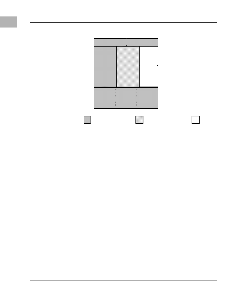
The high availa bility a nd high slot coun t of th e CPX8216 sys tems i s made
possible by implementing two host CPU slots a nd multi ple CompactPCI
bus segments in a single chassis. These bus segments, along with other
system resources are grouped into two logical domains, A and B, which
can be controlle d by either host-HSC pair r egardless of the bus se gment the
host sits on. Domain A includes C ompactPCI bus segment A (sl ots 1 to 8),
the power supply/fan tray modul es and alarm controls. In the CPX8216,
domain B consists of the CompactPCI bus segment B (slots 9 to 16). For
further information on domain c ontrol or ownership, see the section, Hot
Swap Contr oller on page 1-6.
1-1
1
System A rchitecture
Al arm Controls
Domai n A Domain B D om a in A/B
Figure 1-1. CPX8216 Domains
System Layout
The CPX8216 is a 16-slot, high-avail abilit y CompactPCI system with two
separate 6-slot CompactPCI I/ O domains and the capa bility to contain
redundant CPU modules and redundant Hot-Swap Controller (HSC)
modules. It is also possible to configure the sy stem as a simplex, h igh I/O
system containing a single CPU-HSC pair. Eve n as a simplex system, the
CPX8216 still provides improved availability through redundant powe r
supplies and the control/moni toring capabilities of the HSC, as described
in The Hot Swap Controll er/Bridge (HSC) Module on page 1-5.
Bus A Bus B
Power Supply/Fan Trays
Drive
Bays
CPX8216
The CPX8216 standard system consists of two 8-slot subsystems, or
domains, each with two slots for the host proces sor and six slots for
nonhost CompactPCI boards. The HSC board mounts in the rear of the
chassis, behind the s econdar y CPU slot. Figur e 1-2 on pa ge 1-3 pr ovides a
diagram of this configuration.
1-2 Computer Group Literature Center Web Site
CPX8216
Rear Card Locations
Segment A
CPU Transition Module
Segment B
Transition Slots
1234567 9 111213141516
Segment A
I/O Slots
Compact PCI
Segment A
Segment B
CPU Transition Module
Segment B
Front Card Locations
HSC
Segment A
HSC
Segment B
Transition Slots
Segment B
I/O Slots
Compact PCI Bus
Segment B
2450 9812
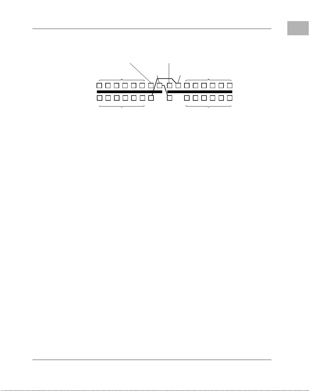
Figure 1-2. CPX8216 Standard System Layout
Each of the two independent I/O domains has its own system processor
slot. Each system processor has direct access to its local bus through an
onboard PCI-to-PCI (P2P) bridge. Each domain is also capable of
supporting a Hot Swap Con troller ( HSC) module that cont ains its own P2P
bridge. Thus, in a f ul ly redunda nt configurati on, there are two bridge s tha t
have access to ea ch of the I/O buses—one assoc iated with the CPU and one
with the HSC. Only one of the bridges may be active at a time, however.
1
http://www.motorola.com/computer/literature 1-3
1
System A rchitecture
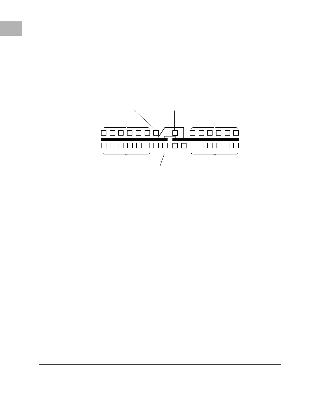
CPX8216T (H.110)
The CPX8216T H.110 system consists of two 8- slot subsystems, or
domains, each with one slot for the host processor, one slot for the frontloaded HSC, and six slots for nonhost CompactPCI boards. F igure 1-3 on
page 1-4 provides a diagram of this configuration.
Rear Card Locations
Segment A
CPU Transition Module
Segment B
CPU Transition Module
Segment B
Transition Slots
1234567 9 111213141516
Segment A
I/O Slots
Compact PCI
Segment A
CPU
A
Segment B
HSC
Front Card Locations
Figure 1-3. CPX8216T H.110 System Layout
Bus Access and Control
In the fully redundant configur ation, the CPU in the left system slot, CPU
A, is associated with the HSC in t he right HSC slot, HSC A (note th at HSC
A actually sits on the Domain B bus). The re is a l ocal connec tion betwe en
each CPU-HSC pair that allows the CPU in one domain to control the other
domain through its HSC. This architecture is illustrated in the following
figure.
810
CPU
B
Segment A
HSC
Segment B
Transition Slots
Segment B
I/O Slots
Compact PCI Bus
Segment B
1-4 Computer Group Literature Center Web Site
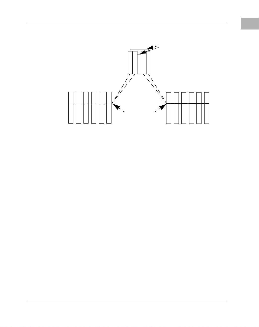
The Hot Swap Controller/B ridge (HSC) Module
S p e c ia l B a c k p la n e
P C I Inte r co n n e c ts
C
H
H
C
P
U
A
S
P
S
C
U
C
A
B
B
1
I/O D o main A
I/O
I/O
S
S
L
L
O
O
T
T
I/O
I/O
I/O
I/O
S
S
S
L
L
O
O
T
T
S
L
L
O
O
T
Primary CompactPCI
T
Buses
I/O D o m a in B
I/O
I/O
S
S
L
L
O
O
T
T
I/O
I/O
I/O
I/O
S
S
S
L
L
O
O
T
T
S
L
L
O
O
T
T
Figure 1-4. CPX8216 I/O Bus Connectivity
In addition to provi ding bridges t o the remote I/O bus es, the HSC provides
the services necessar y to hot swap CPU boards and nonhost proces sor
boards and also contro ls the system ala rm panel, fans, and power suppli es.
The Hot Swap Controller/Bridge (HSC) Module
The HSC module connect s to the CPU module through a loc al P CI bus, as
illustrated in Figure 1-2 and Figure 1-3. The HSC module contains a PCI-
to-PCI bridge and also contains a Hot Swap Controller .
The functionalit y provided by the HSC is at the heart of the High
Ava ilability CPX8216 System. Its primary functions include:
❏ Providing a bridge between the two ei ght-slot CompactPCI buses
so that they can be managed by a single CPU module
❏ Maintaining a Control Status Register whi ch contains in formation
on the status of each system module
http://www.motorola.com/computer/literature 1-5

1
System A rchitecture
❏ Controlling power and resets to each system module through
radial connections
❏ Monitoring and controlling CPU boards, nonhost boar ds, a nd
peripherals, including power and fan sleds, board and system
LEDs, and alarms
Hot Swap Controller
Each of the nonhost slots in the syste m can be controlled from either HSC.
When an HSC has control over a domain it has control over the nonhost
boards in that domain. Each host processor /br idge pair is controlled as a
single item by the other processor/bridge pair. The bridge and the host
processor are linked together so tha t both must be present for power to be
applied. A host processor cannot be operate d without its HSC.
With the CPX8216 a rchitectur e it is importa nt that the syste m initializes t o
a state that allows the host processor s and HSCs to be in control of the
system. The default conditions are:
❏ System processors an d bridges are powered up (if present)
❏ System processors an d bridges are disconne cted from their busses
❏ HSCs are not in control of either domain
❏ Nonhost boards are powered off
❏ Peripheral bay s are pow e red u p (if pres en t)
❏ Fans and power supplies are powere d on
Note System components such as fans and power supplies may be
controlled by e ither HSC but not both. Def ault cont rol belongs to
Domain A and whichever HSC has control of Domain A has
control of the system functions .
If Domain A is not controlled, nonhost boards are powere d- off
and all LED updates to the display panel and power supplies are
suspended. Also, monitoring of alarm inputs from the display
panel and power supplies are inhibited.
1-6 Computer Group Literature Center Web Site

System Process o r Config urati o n s
Subsequent to the default, the system software must determine the
configuration of the system and then proceed to change it.
System Processor Configurations
The CPX8216 is a flexib le system that allows for multiple configurations
of processor control, I/O redundancy, and peripheral configur ations. The
following sections br iefly touch on possible configurati ons.
As noted above, there are three possible processor/control configurations:
❏ A simplex system conta ining a single CPU-HSC pair controlling
both I/O domains
❏ An active/pa ssive configuration simila r to the simpl ex
configuration , but providing a warm backup for bot h the CPU and
the HSC
❏ An active/active or load-sharing configuration in which each CPU
runs a single domain while also serving a s a backup to the othe r
CPU.
Note H.110 traffic and HA Linux do not support a load-
sharing configura tion.
1
The following sections give a general de scription of these configurations.
The Simplex Configuration
Because of the flexible nature of the CPX8216, it is possible to configure
it with different lev el s of redundancy and availability. For applications
which do not require the benefits of full high availability, it is possible to
configure the CPX8216 as a simplex, 16-slot system. This configuration
provides the benefits of redundant power supplies and the system
monitoring capabilities of the fully redundant configuration.
http://www.motorola.com/computer/literature 1-7
1
System A rchitecture
The simplex configuration is illustrated in the following figure.
I/O D o main A
I/O
I/O
I/O
I/O
I/O
I/O
S
S
S
S
S
L
L
L
O
T
L
O
O
O
T
T
T
S
L
L
O
O
T
T
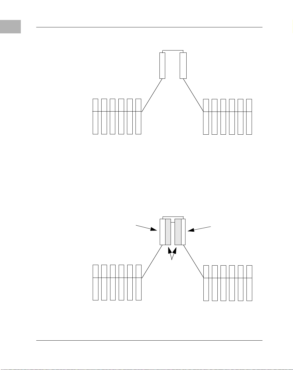
The Activ e/Pa ssive Configu r ati on
In the active/passi ve configuration , one CPU manages all twelve I/ O slots,
much like in the simplex confi guration. In addition, th e second CPU serves
as a warm standby, ready to run the system in the event of a failure on the
active system.
The active/passive confi gur ation is illustrated in the following figure.
Active CPU
C
P
U
A
H
S
C
A
I/O D o main B
I/O
I/O
I/O
I/O
I/O
I/O
S
S
S
S
S
L
L
L
O
O
T
T
C
H
H
C
P
U
A
S
P
S
C
U
C
A
B
B
Activ e HS C
L
O
O
T
T
S
L
L
O
O
T
T
I/O Domain A
Passive
I/O Domain B
CPU/HS C
I/O
I/O
I/O
I/O
I/O
I/O
S
S
S
S
S
L
L
O
T
L
O
O
O
T
T
S
L
L
L
O
O
T
T
T
I/O
I/O
I/O
I/O
I/O
I/O
S
S
S
S
S
L
L
L
O
O
T
T
L
O
O
T
T
S
L
L
O
O
T
T
1-8 Computer Group Literature Center Web Site
The Active/Active or Load-Sharing Configuration
The Active/Ac tive or Load-Sharing Confi guration
In the load sharing configu ration, each CPU manages si x of the twelve I/O
slots, much like a dual 8-slot system with the added benefit of one CPU
being able to control all twelve I/O slots if the other CPU fails. It is
important in a load-shar ing configuration to note that the total cri tical
activity does not exceed the capabilities of a single CPU, because either
one of the C PUs must be ready to take over the loa d carried by the other.
The active/activ e confi guration is illustrated in the following figure.
H
C
H
C
P
S
S
P
U
A
C
U
C
AB
B
1
I/O D o main A
I/O
I/O
S
S
L
L
O
O
T
T
I/O
I/O
I/O
I/O
S
S
S
L
L
O
O
T
T
S
L
L
O
O
T
T
I/O D o m a in B
I/O
I/O
S
S
L
L
O
O
T
T
I/O
I/O
I/O
S
S
L
O
T
S
L
L
O
O
T
T
Note H.110 traffic and HA Linux do not support a load-sharing
configuration .
I/O
S
L
O
T
http://www.motorola.com/computer/literature 1-9

1
System A rchitecture
I/O Configurations
The CPX8216 contains two independent 8-slot Co mpactPCI buses. One
slot in each bus is dedicated to a system processor, and another is needed
for the HSC. This leaves six slots on each bus to support I/O devic es or
nonsystem processors.
One possible configuration is to use the CPX8216 as a high I/O
CompactPCI system with redundant CPUs. With this configuration, it is
possible to run twelve independent I /O modul es within a CPX8216
system. Applications requiring dense processing power could use all
twelve I/O slots to support nonsystem processors.
Such a system would be protecte d against a CPU or HSC fault, but it would
be vulnerable to data losses if any of the I/O modules or nonsystem
processor modules were to fail. In syste ms handling critical data, it is
possible to implement a 2N or an N+1 I/O redundancy str ategy that allows
the level of service to be continued in the event that a module fails.
In the case of a 2N-redundant system, each I/O module or nonsystem
processor module is matched with an identical module on the other bus.
The paired modules can be configur ed in an active/passi ve arrangement or
a load-sharing arrangement in wh ic h each carri es h al f of the load of a
single module. In an N+1 ar rangement, multi ple modules a re backed up by
a single spare. For example, a single passive nonsystem processor module
can be used to back up five others.
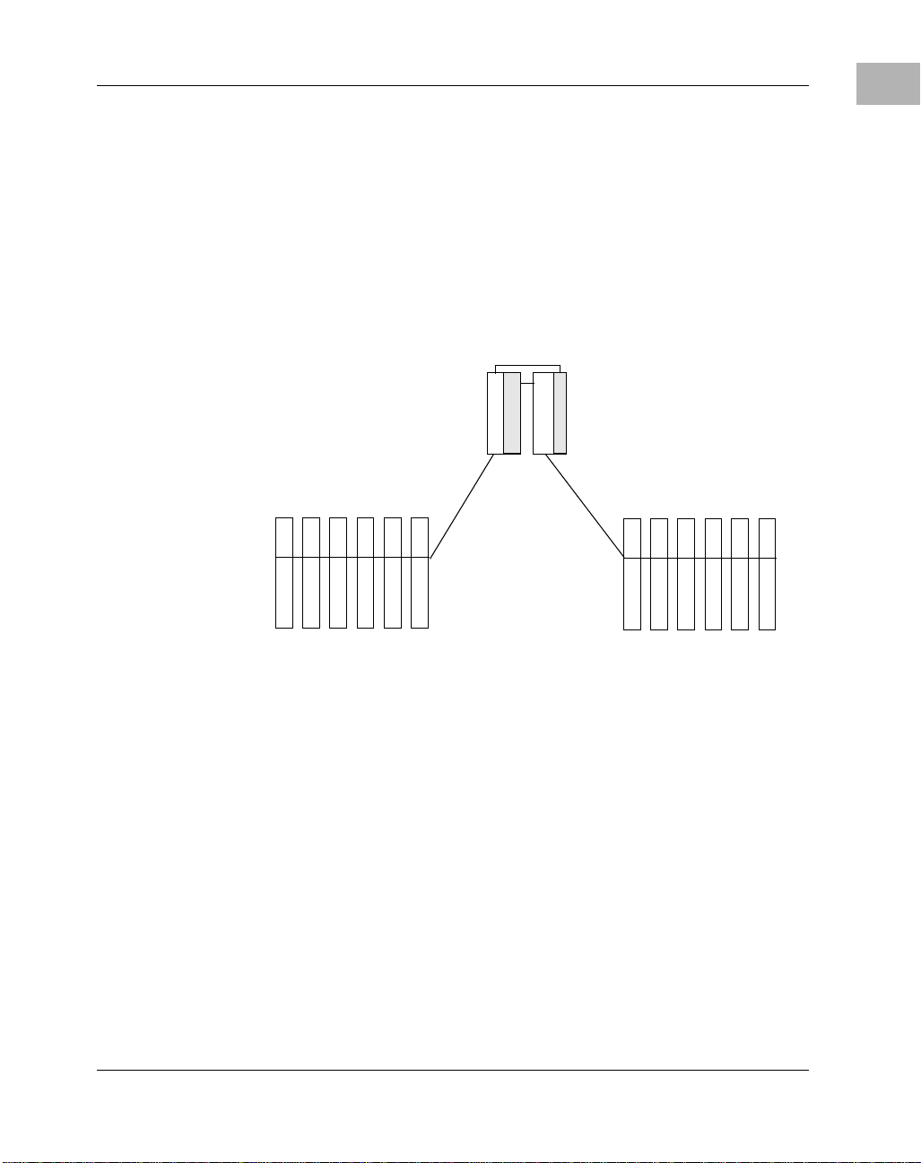
Peripherals
Power/Fan Modules
The CPX8216 system requires a minimum of two power/fan sled modules
and a fan-only sled module to provide adequate power and cooling for a
fully loaded, nonredundant system. The system can c onta in a third power
supply/fan sled a s part of an N+1 strategy, meaning that the system can
continue providing se rvice if one of the mod ules fails. These modules are
hot swappable and available for DC and AC environments.
1-10 Computer Group Liter ature Center Web Site
Loading...