


CXA1352AS
2-channel 5 Elements Graphic Equalizer IC
Description
The CXA1352AS is a bipolar IC for graphic equalizer use. All controls are DC performed while the addition of single-potentiometers easily composes a 2-channel graphic equalizer.
Features
•Microcomputer control possible
•Built-in electronic volume
•Built-in pseudo loudness function
•Built-in balance function
•Each channel corresponds to 5 elements
•2 channels of FIX OUT and LINE OUT pins
Applications
22 pin SDIP (Plastic)
Absolute Maximum Ratings (Ta=25 °C) |
|
||
• Supply voltage |
VCC |
12 |
V |
• Storage temperature |
Tstg |
–65 to +150 |
°C |
• Allowable power dissipation |
|
|
|
|
PD |
1200 |
mW |
Graphic equalizer for cassette tape recorder with |
|
|
|
|
Operating Conditions |
|
|
|
|
radio, mobile stereo and portable stereo |
VCC |
4.0 to 10.0 |
V |
|
• Supply voltage |
||||
Structure |
DVCC |
3.5 to VCC |
V |
|
Topr |
–20 to +75 |
°C |
||
• Operating temperature |
Bipolar silicon monolithic IC
Block Diagram and Pin Configuration
1kHz |
4kHz |
10kHz |
DVCC |
DC2 |
IN2 |
VCC |
LINE OUT2 |
OUT2 (FIX) |
OUT2 |
(VARIABLE) |
VG |
22 |
21 |
20 |
19 |
18 |
17 |
16 |
15 |
14 |
13 |
12 |
|
|
|
|
|
|
14dB |
29dB |
|
|
|
|
|
|
|
|
|
|
|
|
|
|
VOLUME |
||
|
|
|
|
|
|
|
|
|
|
||
|
|
|
|
|
|
GRAPHIC EQUALIZER |
|
|
|
||
|
CONTROL |
|
|
|
|
|
|
|
|
|
BIAS |
|
|
|
|
|
|
GRAPHIC EQUALIZER |
|
|
|
||
|
|
|
|
|
14dB |
29dB |
|
|
|
|
|
|
|
|
|
|
|
|
|
VOLUME |
|||
|
|
|
|
|
|
|
|
|
|
||
1 |
2 |
3 |
4 |
5 |
6 |
7 |
8 |
9 |
10 |
11 |
|
400Hz |
100Hz |
BAL |
VOL |
DC1 |
1N1 |
GND |
LINE OUT1 |
OUT1 (Fix) |
OUT1 |
(VARIABLE) |
ISET |
Sony reserves the right to change products and specifications without prior notice. This information does not convey any license by any implication or otherwise under any patents or other right. Application circuits shown, if any, are typical examples illustrating the operation of the devices. Sony cannot assume responsibility for any problems arising out of the use of these circuits.
—1—
E91912B95-TE
|
|
|
|
|
|
|
|
CXA1352AS |
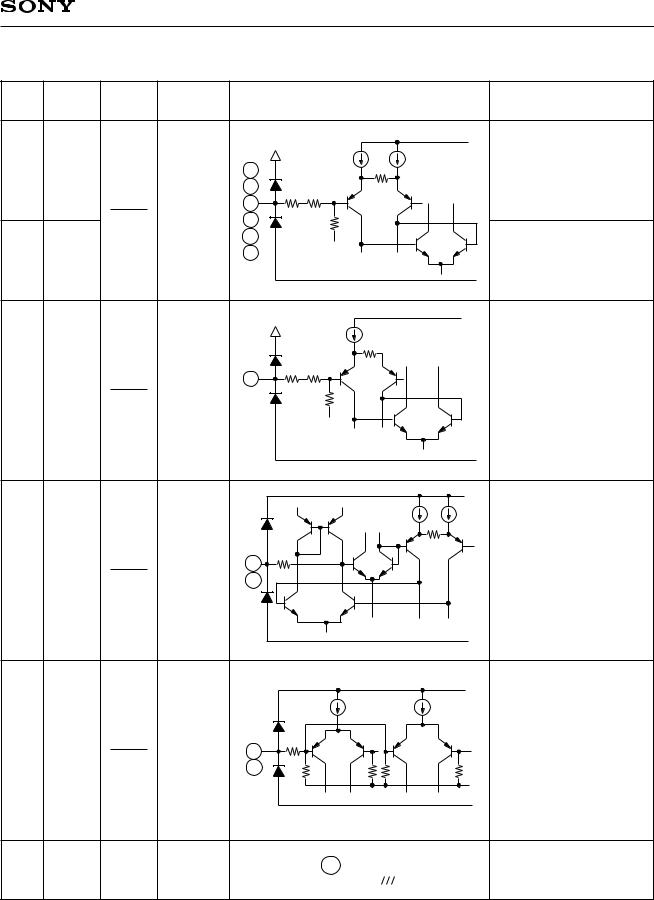
Pin Description |
|
|
|
|
|
|
|
|
Pin |
Symbol |
Voltage |
I/O |
|
Equivalent circuit |
|
Description |
|
No. |
resistance |
|
|
|||||
|
|
|
|
|
|
|
||
1 |
400 Hz |
|
|
|
|
|
|
Graphic equalizer control |
2 |
100 Hz |
|
|
DVCC |
|
|
VCC |
|
|
|
|
|
|
||||
|
|
|
|
|
pin |
|||
20 |
10 kHz |
|
|
1 |
|
|
|
|
|
|
|
|
|
|
|||
21 |
4 kHz |
|
|
2 |
40k |
10k |
|
|
DVCC |
|
147 |
|
|
DC input |
|||
22 |
1 kHz |
60 kΩ |
4 |
|
|
|
||
2 |
20 |
20k |
|
|
|
|||
|
|
|
|
|
|
|||
|
|
|
|
21 |
|
|
|
Volume control pin |
4 |
VOL |
|
|
22 |
|
|
|
|
|
|
|
|
|
|
DC input |
||
|
|
|
|
|
|
|
GND |
|
|
|
|
|
DVCC |
|
|
VCC |
|
|
|
|
|
|
|
|
|
|
|
|
|
|
|
9k |
|
|
|
|
|
DVCC |
|
147 |
40k |
|
|
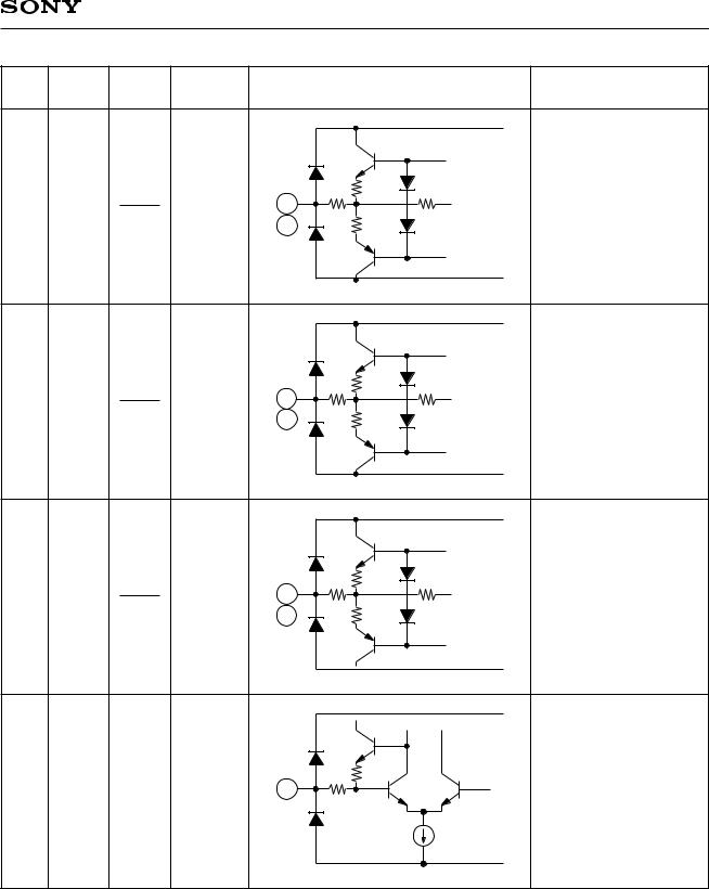
Balance control pin |
3 |
BAL |
60 kΩ |
3 |
|
|
|
||
2 |
|
20k |
|
|
DC input |
|||
|
|
|
|
|
|
|||
|
|
|
|
|
|
|
GND |
|
|
|
|
|
|
|
|
VCC |
|
|
|
|
|
|
|
|
30k |
Connects the DC |
5 |
DC1 |
VCC |
|
147 |
|
|
|
feedback capacitor of the |
— |
5 |
|
|
|
||||
18 |
DC2 |
2 |
18 |
|
|
|
LPF used in the 100 Hz |
|
|
|
|
|
|||||
|
|
|
|
|
|
|
|
graphic equalizer |
|
|
|
|
|
|
|
GND |
|
|
|
|
|
|
|
|
VCC |
|
6 |
IN1 |
VCC |
25 kΩ |
147 |
|
|
|
Signal input pin |
17 |
IN2 |
2 |
6 |
|
|
|
||
|
17 |
50k |
|
|
|
|||
|
|
|
|
5k |
50k |
1k |
|
|
|
|
|
|
|
|
|||
|
|
|
|
|
|
|
GND |
|
7 GND |
GND |
7 |
|
|
|
GND pin |
|
|
|
—2—
CXA1352AS
Pin |
Symbol |
I/O |
|
Equivalent circuit |
Description |
||
No. |
Voltage |
|
|||||
|
resistance |
|
|
|
|
|
|
|
|
|
|
|
|
|
VCC |
8 |
L OUT1 |
VCC |
|
147 |
300 |
27k |
|
|
|
Line output pin |
|||||
15 |
L OUT2 |
0 |
8 |
|
|
|
|
2 |
15 |
|
300 |
|
|
||
|
|
|
|
|
|
||
|
|
|
|
|
|
|
GND |
|
|
|
|
|
|
|
VCC |
9 |
F OUT1 |
VCC |
|
|
147 |
300 |
30k |
0 |
9 |
|
|||||
14 |
F OUT2 |
2 |
|
|
Fix output pin |
||
|
14 |
|
300 |
|
|||
|
|
|
|
|
|
||
|
|
|
|
|
|
|
GND |
|
|
|
|
|
|
|
VCC |
|
|
|
|
|
|
250 |
Electronic volume output |
10 |
OUT1 |
VCC |
|
|
147 |
20k |
|
0 |
|
|
|||||
13 |
OUT2 |
2 |
10 |
|
|
pin |
|
|
13 |
|
250 |
|
|||
|
|
|
|
|
|
||
|
|
|
|
|
|
|
GND |
|
|
|
|
|
|
|
VCC |
|
|
|
|
|
|
|
Reference current setting |
|
|
|
|
|
147 |
300 |
pin |
11 |
ISET |
1.3 V |
0 |
11 |
|
(for graphic equalizer) |
|
|
|
||||||
|
|
|
|
|
|
|
Normally 160 kΩ resistor |
|
|
|
|
|
|
|
is connected |
|
|
|
|
|
|
|
GND |
—3—
|
|
|
|
|
CXA1352AS |
Pin |
Symbol |
Voltage |
I/O |
|
Description |
No. |
Equivalent circuit |
|
|||
|
|
resistance |
|
|
|
|
|
|
|
VCC |
|
|
|
|
40k |
|
Signal reference voltage |
|
|
|
|
|
|
12 |
VG |
VCC |
147 |
300 |
pin |
2 |
20 kΩ |
|
A capacitor is connected |
||
|
|
12 |
300 |
||
|
|
|
40k |
|
for ripple rejection |
|
|
|
|
|
|
|
|
|
|
GND |
|
16 |
VCC |
VCC |
|
16 |
VCC |
Power supply pin |
|
|
|||||
|
|
|
(operation) |
|||
|
|
|
|
|
|
|
|
|
|
|
19 |
DVCC |
|
|
|
|
|
|
VCC |
|
19 |
DVCC |
DVCC |
60 kΩ |
30k |
|
Power supply pin (control) |
|
|
|||||
|
|
|
|
30k |
42k |
|
|
|
|
|
|
GND |
|
—4—

CXA1352AS
Electrical Characteristics |
|
|
(Ta=25 °C, VCC=8 V, DVCC=5 V) |
|||||
|
|
|
|
|
|
|
|
|
No. |
Item |
Symbol |
Test conditions |
|
Min. |
Typ. |
Max. |
Unit |
1 |
Supply voltage |
VCC |
|
|
4.0 |
— |
10.0 |
V |
(operation) |
|
|
||||||
|
|
|
|
|
|
|
|
|
|
|
|
|
|
|
|
|
|
2 |
Supply voltage |
DVCC |
|
|
3.5 |
— |
VCC |
V |
(control) |
|
|
||||||
|
|
|
|
|
|
|
|
|
|
|
|
|
|
|
|
|
|
3 |
Current consumption |
ICC |
Graphic equalizer ALL FLAT, |
|
8.0 |
12.0 |
16.0 |
mA |
Volume MID |
|
|||||||
|
|
|
|
|
|
|
|
|
4 |
Reference input level |
VIN |
|
|
— |
–34.0 |
— |
dBm |
|
|
|
|
|
|
|
|
|
5 |
Reference output level |
VOUT |
Graphic equalizer ALL FLAT, |
|
–23.0 |
–20.0 |
–17.0 |
dBm |
Volume MAX, f=1 kHz |
|
|||||||
|
|
|
|
|
|
|
|
|
|
|
|
|
|
|
|
|
|
6 |
Reference LINE |
VLINE |
f=1 kHz |
|
–6.5 |
–4.5 |
–2.5 |
dBm |
output level |
|
|||||||
|
|
|
|
|
|
|
|
|
7 |
Reference FIX |
VFIX |
Graphic equalizer ALL FLAT, |
|
–23.0 |
–20.0 |
–17.0 |
dBm |
output level |
f=1 kHz |
|
||||||
|
|
|
|
|
|
|
||
8 |
Graphic equalizer |
GEQ1 |
LPF cut off frequency (–3 dB) |
|
— |
200 |
— |
Hz |
setting frequency (1) |
|
|||||||
|
|
|
|
|
|
|
|
|
9 |
Graphic equalizer |
GEQ2 |
BPF (1) central frequency |
|
— |
400 |
— |
Hz |
setting frequency (2) |
|
|||||||
|
|
|
|
|
|
|
|
|
10 |
Graphic equalizer |
GEQ3 |
BPF (2) central frequency |
|
— |
1.0 |
— |
kHz |
setting frequency (3) |
|
|||||||
|
|
|
|
|
|
|
|
|
|
|
|
|
|
|
|
|
|
11 |
Graphic equalizer |
GEQ4 |
BPF (3) central frequency |
|
— |
4.0 |
— |
kHz |
setting frequency (4) |
|
|||||||
|
|
|
|
|
|
|
|
|
12 |
Graphic equalizer |
GEQ5 |
HPF cut off frequency (–3 dB) |
|
— |
8.0 |
— |
kHz |
setting frequency (5) |
|
|||||||
|
|
|
|
|
|
|
|
|
|
|
|
|
|
|
|
|
|
13 |
Graphic equalizer |
EQ |
Cut off frequency and central |
|
–20 |
0 |
20 |
% |
frequency deviation |
frequency deviation |
|
||||||
|
|
|
|
|
|
|
||
14 |
Maximum boost (1) |
GEQB1 |
f=400 Hz, 1 kHz, 4 kHz |
|
9.0 |
11.2 |
14.0 |
dB |
maximum boost |
|
|||||||
|
|
|
|
|
|
|
|
|
15 |
Maximum boost (2) |
GEQB2 |
f=100 Hz, 10 kHz maximum boost |
|
8.0 |
10.7 |
14.0 |
dB |
|
|
|
|
|
|
|
|
|
16 |
Maximum cut (1) |
GEQC1 |
f=400 Hz, 1 kHz, 4kHz |
|
–13.0 |
–10.7 |
–8.5 |
dB |
maximum cut |
|
|||||||
|
|
|
|
|
|
|
|
|
17 |
Maximum cut (2) |
GEQC2 |
f=100 Hz, 10 kHz maximum cut |
|
–12.0 |
–9.5 |
–7.0 |
dB |
RL=2 kΩ , Graphic equalizer |
|
|||||||
|
|
|
|
|
|
|
|
|
18 |
Total harmonic |
THD |
ALL FLAT, Volume MAX, f=1 kHz, |
|
— |
0.25 |
1.0 |
% |
|
|
|||||||
distortion |
Reference +10 dB is input |
|
||||||
|
|
|
|
|
|
|
||
19 |
Volume attenuation (1) |
VOL1 |
Graphic equalizer ALL FLAT, |
|
–1.5 |
0 |
1.5 |
dB |
Volume MAX, f=1 kHz |
|
|||||||
|
|
|
|
|
|
|
|
|
20 |
Volume attenuation (2) |
VOL2 |
Graphic equalizer ALL FLAT, |
|
— |
–94.4 |
–80.0 |
dB |
Volume MIN, f=1 kHz |
|
|||||||
|
|
|
|
|
|
|
|
|
21 |
Balance adjustment (1) |
BAL1 |
Graphic equalizer ALL FLAT, |
|
— |
0 |
— |
dB |
BAL=MAX,Volume MAX, f=1kHz |
|
|||||||
|
|
|
|
|
|
|
|
|
22 |
Balance adjustment (2) |
BAL2 |
Graphic equalizer ALL FLAT, |
|
— |
–66 |
— |
dB |
BAL=MIN, Volume MAX, f=1kHz |
|
|||||||
|
|
|
|
|
|
|
|
|
23 |
Noise level |
VNOIS |
Rg=5 kΩ , Graphic equalizer ALL |
|
— |
–93.1 |
–88.0 |
dB |
FLAT, Volume MAX, “A” WTG filter |
|
|||||||
|
|
|
|
|
|
|
|
|
|
|
|
|
|
|
|
|
|
24 |
Output offset voltage |
VOFF |
Graphic equalizer ALL FLAT, |
|
3.5 |
4.0 |
4.5 |
V |
Volume MAX |
|
|||||||
|
|
|
|
|
|
|
|
|
|
|
|
|
|
|
|
|
|
—5—

Electrical Characteristics Test Circuit |
|
|
|
|
|
|
|
|
|
|
|
|
|
|
|
||||
|
|
|
|
|
|
GND |
|
|
|
|
|
|
|
|
|
|
|
||
|
|
|
|
|
POWER |
|
POWER |
|
|
|
|
|
|
|
|
S10 |
DC |
||
|
|
|
|
|
SUPPLY |
|
SUPPLY |
|
|
|
|
|
|
|
|
VOLTMETER |
|||
|
|
|
|
|
|
|
|
|
|
|
|
|
|
|
|
|
|
S9 |
|
BOOST |
CUT |
|
|
|
|
|
|
|
|
|
|
|
|
|
|
|
|
S8 |
|
|
|
|
|
|
|
|
|
|
|
|
|
|
|
|
|
||||
R7 |
|
|
|
|
|
|
|
|
|
C13 |
|
|
|
R14 |
|
R16 |
C20 |
S4 |
|
|
|
|
|
|
|
|
|
|
|
|
|
|
47 / |
|
|||||
|
|
|
|
|
|
|
|
100 / |
|
|
|
|
|
|
|||||
50k |
|
|
|
C8 |
|
S2 |
A |
25V |
|
|
|
20k |
|
20k |
25V |
R20 |
|
||
|
|
|
|
|
100 / |
|
|
|
|
|
|
|
|
|
|
|
|
||
|
|
|
|
|
|
|
|
|
|
|
|
|
|
|
R19 |
2k |
|
||
|
|
|
|
|
25V |
|
R10 |
|
|
|
|
|
|
|
|
|
|||
|
|
|
|
|
|
|
|
|
|
|
|
|
|||||||
BOOST |
CUT |
C2 |
C4 |
C6 |
|
|
39k |
R12 |
|
|
|
|
|
|
|
20k |
S16 |
|
|
R6 |
|
1000p |
1000p |
1000p |
|
|
|
C15 |
|
|
|
|
|
|
|
||||
|
|
|
|
|
C10 |
|
5.1k |
|
|
|
|
|
|
S15 |
|
||||
50k |
|
|
|
|
4.7 / |
|
4.7 |
|
|
|
|
|
|
|
|
||||
|
|
|
|
|
|
25V |
|
C12 |
/25V |
C17 |
|
|
|
S14 |
|
||||
|
|
|
|
|
|
|
4.7 / |
|
|
4.7 |
|
|
C19 |
|
|
|
|||
|
|
|
|
|
|
|
|
|
25V |
|
|
/25V |
|
|
|
S20 |
|||
|
|
|
|
|
|
|
|
|
|
|
|
|
|
4.7 /25V |
|
|
|||
BOOST |
CUT |
22 |
21 |
20 |
19 |
18 |
|
17 |
16 |
15 |
|
14 |
|
13 |
12 |
|
1kHz BPF |
||
|
|
|
|
|
|||||||||||||||
R5 |
|
1kHz |
4kHz |
10kHz |
DVCC |
DC2 |
|
IN2 |
VCC |
OUT2 |
|
OUT2 |
|
OUT2 |
VG |
|
S19 |
||
50k |
|
|
|
|
|||||||||||||||
|
|
|
|
|
|
|
|
|
|
|
|
|
|
|
|
|
|
|
DIN AUDIO |
|
|
|
|
|
|
|
|
|
|
L |
|
F |
|
|
|
|
|
|
|
—6— |
|
|
|
|
|
CXA1352AS |
|
|
|
|
|
|
|
|
|
S18 |
|||
|
|
|
|
|
|
|
|
|
|
|
|
|
|
|
|
|
|
||
|
400Hz |
100Hz |
BAL |
VOL |
DC1 |
|
IN1 |
GND |
OUT1L |
|
OUT1F |
|
OUT1 |
ISET |
|
“A” WTG |
|||
|
|
|
|
|
|
||||||||||||||
R4 |
|
|
|
|
|
|
|
|
|
|
|
|
|
|
|
|
|
|
|
50k |
|
|
|
|
|
|
|
|
|
|
|
|
|
|
|
|
|
NOISE FILTER |
|
BOOST |
CUT |
1 |
2 |
3 |
4 |
5 |
|
6 |
7 |
8 |
|
9 |
|
10 |
11 |
OUT |
IN |
||
|
|
|
|
|
|
|
|
|
C11 |
|
|
|
|
|
|
C18 |
|
||
|
|
|
|
|
|
|
|
|
|
|
|
|
|
|
S17 |
FILTER |
|||
|
|
|
|
|
|
C9 |
|
4.7 / |
|
|
|
C16 |
4.7 /25V |
|
|||||
|
|
|
|
|
|
|
|
|
|
|
S13 |
|
|||||||
R3 |
|
|
|
|
|
|
|
|
25V |
|
|
4.7 /25V |
|
|
|
|
|||
|
|
|
|
|
4.7 / |
|
|
|
|
|
|
S12 |
|
||||||
50k |
|
|
|
|
25V |
|
|
|
|
|
|
|
|
|
|
AC |
|||
|
|
|
|
|
|
|
|
|
|
|
|
|
|
|
|
|
|||
BOOST |
CUT |
C1 |
C3 |
|
|
|
R9 |
|
|
|
|
|
|
|
|
|
S11 |
||
|
|
|
|
|
|
|
|
|
|
|
|
VOLTMETER |
|||||||
|
|
1000p |
1000p |
|
|
|
39k |
R11 |
C14 |
|
|
|
|
|
|
R21 |
|
||
|
|
|
|
C5 |
C7 |
|
|
|
|
|
|
|
|
|
|
||||
|
|
|
|
|
|
|
5.1k |
4.7 /25V |
|
|
|
|
|
2k |
|
||||
R2 |
|
|
|
1000p |
1000p |
|
S1 |
|
R13 |
|
R15 |
R17 R18 |
|
||||||
|
|
|
|
|
|
|
|
|
|
|
DISTORTION |
||||||||
|
|
|
|
|
|
|
|
|
|
|
|
|
|||||||
50k |
|
|
|
|
|
|
|
|
|
|
|
|
20k |
|
20k |
160k 20k |
|
||
|
|
|
|
|
|
|
|
|
|
|
|
|
S3 |
ANALYZER |
|||||
|
|
|
|
|
|
|
|
|
|
|
|
|
|
|
|||||
CH2 |
CH1 |
|
|
|
|
|
|
|
|
|
|
|
|
|
|
|
|
||
|
|
|
|
|
|
|
|
|
|
|
|
|
|
|
|
|
|
||
|
|
|
|
|
|
|
|
|
|
|
|
|
|
|
|
|
|
S7 |
|
R1 |
|
|
|
|
|
|
|
|
|
|
|
|
|
|
|
|
|
S6 |
OSCILLO |
|
|
|
|
|
|
|
|
|
|
|
|
|
|
|
|
|
|
||
50k |
|
|
|
|
|
|
|
|
|
|
|
|
|
|
|
|
S5 |
–SCOPE |
|
MAX |
MIN |
R8 |
|
|
|
|
|
|
NOTE |
|
|
|
|
|
|
|
|
|
|
|
|
|
|
|
|
|
|
1. RESISTOR TOLERANCE |
±5% |
|
|
||||||||
|
|
620 |
|
|
|
|
|
|
|
CXA1352AS |
|||||||||
|
|
|
|
|
|
|
|
|
|
|
|
|
|
|
±1% |
|
|||
|
|
|
|
|
|
|
|
|
|
|
|
|
|
|
|
|
|||
|
|
|
|
|
|
|
|
|
2. CAPACITOR TOLERANCE ±5% |
|
|||||||||
|
AUDIO |
|
|
|
|
|
|
|
|
|
|
|
|
|
±2% |
|
|
||
|
SG |
|
|
|
|
|
|
|
|
COUPLING CAPACITPR |
±10% |
|
|
||||||
 Loading...