


CXA1691BM/BS
FM/AM Radio
For the availability of this product, please contact the sales office.
Description
CXA1691BM/BS is a one-chip FM/AM radio IC designed for radio-cassette tape recorders.
Features
•Small number of peripheral components.
•Low current consumption (VCC=3 V)
For FM : ID=5.8 mA (Typ.)
For AM : ID=4.7 mA (Typ.)
•Built-in FM/AM select switch.
•Large output of AF amplifier.
VCC=6 V, EIAJ output=500 mW (Typ.) when load impedance 8 Ω
Function
FM section
•RF amplifier, Mixer and OSC (incorporating AFC variable capacitor).
•IF amplifier
•Quadrature detection
•Tuning LED driver
AM section
•RF amplifier, Mixer and OSC (with RF AGC)
•IF amplifier (with IF AGC)
•Detector
•Tuning LED driver
AF section
•Electronic volume control
•FM muting
Structure
Bipolar monolithic IC
CXA1691BM |
CXA1691BS |
28 pin SOP (Plastic) |
30 pin SDIP (Plastic) |
Absolute Maximum Ratings (Ta=25 °C) |
|
||
• Supply voltage |
VCC |
14 |
V |
• Operating temperature |
Topr |
–10 to +60 |
°C |
• Storage temperature |
Tstg |
–50 to +125 |
°C |
• Allowable power dissipation |
|
|
|
|
PD |
700 |
mW |
|
|
(CXA1691BM) |
|
|
PD |
1000 |
mW |
|
|
(CXA1691BS) |
|
Recommended Operating Conditions |
|
||
Supply voltage |
VCC |
2 to 7.5 |
V |
|
|
(CXA1691BM) |
|
|
VCC |
2 to 8.5 |
V |
|
|
(CXA1691BS) |
|
Sony reserves the right to change products and specifications without prior notice. This information does not convey any license by any implication or otherwise under any patents or other right. Application circuits shown, if any, are typical examples illustrating the operation of the devices. Sony cannot assume responsibility for any problems arising out of the use of these circuits.
—1—
E99215-TE
CXA1691BM/BS
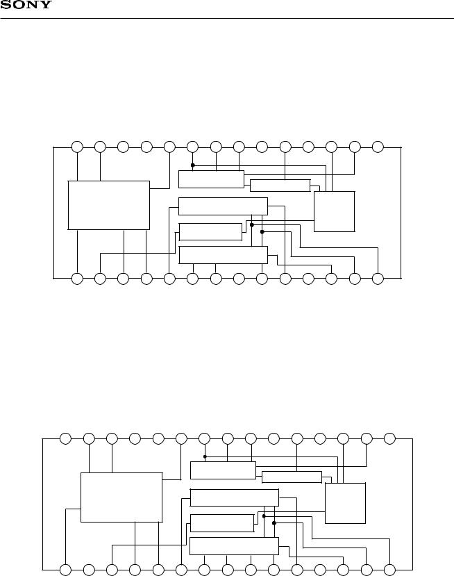
Block Diagram
CXA1691BM
|
AF |
|
|
|
|
|
|
|
|
|
|
|
FM/AM |
|
|
Ripple |
AF |
DET |
AFC |
AFC |
IF |
|
|
FM |
AM |
BAND |
|
GND |
OUT |
VCC FILTER |
IN |
OUT |
AGC |
AGC |
GND METER NC |
IF IN |
IF IN SELECT |
||||
28 |
27 |
26 |
25 |
24 |
23 |
22 |
21 |
20 |
19 |
18 |
17 |
16 |
15 |
|
|
|
|
|
AM IF DET AGC |
TUNING METER |
|
|
|
||||
|
|
|
|
|
|
|
|
|
|
|
|||
AF POWER AMP |
|
|
AM FE |
|
|
|
FM IF |
|
|
||||
|
|
|
|
|
|
|
|
|
|
|
|
|
|
|
|
|
|
|
|
FM |
|
|
|
|
|
|
|
|
|
|
|
|
DISCRIMINATOR |
|
|
|
|
|
|
||
|
|
|
|
|
|
FM FE |
|
|
|
|
|
|
|
1 |
2 |
3 |
4 |
5 |
6 |
7 |
8 |
9 |
10 |
11 |
12 |
13 |
14 |
MUTE |
FM |
NF |
VOL |
AM |
AFC |
FM |
Reg |
FM |
AM |
NC |
FM |
FE |
FM/AM |
|
DISCRI |
|
|
OSC |
|
OSC |
OUT |
RF |
RF IN |
|
RF IN GND FE OUT |
||
CXA1691BS
|
|
AF |
|
|
|
|
|
|
|
|
|
|
|
FM/AM |
|
|
|
Ripple |
AF |
DET |
AFC |
AFC |
IF |
|
|
FM |
AM |
BAND |
|
GND |
GND |
OUT |
VCC FILTER |
IN |
OUT |
AGC |
AGC |
GND METER |
NC |
IF IN |
IF IN SELECT |
|||
30 |
29 |
28 |
27 |
26 |
25 |
24 |
23 |
22 |
21 |
20 |
19 |
18 |
17 |
16 |
|
|
|
|
|
|
AM IF DET AGC |
TUNING METER |
|
|
|
||||
|
|
|
|
|
|
|
|
|
|
|
|
|||
|
AF POWER AMP |
|
|
AM FE |
|
|
|
FM IF |
|
|
||||
|
|
|
|
|
|
|
|
|
|
|
|
|
|
|
|
|
|
|
|
|
|
FM |
|
|
|
|
|
|
|
|
|
|
|
|
|
DISCRIMINATOR |
|
|
|
|
|
|
||
|
|
|
|
|
|
|
FM FE |
|
|
|
|
|
|
|
1 |
2 |
3 |
4 |
5 |
6 |
7 |
8 |
9 |
10 |
11 |
12 |
13 |
14 |
15 |
MUTE |
NC |
FM |
NF |
VOL |
AM |
AFC |
FM |
Reg |
FM |
AM |
NC |
FM |
FE |
FM/AM |
|
|
DISCRI |
|
|
OSC |
|
OSC |
OUT |
RF |
RF IN |
|
RF IN GND FE OUT |
||
—2—
|
|
|
|
|
|
|
|
|
CXA1691BM/BS |
|
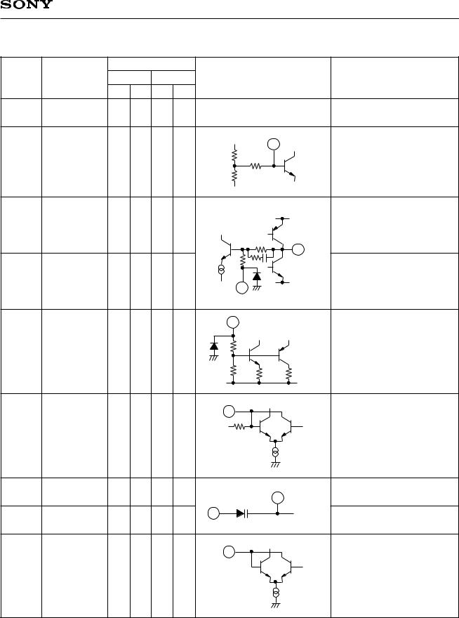
Standard Circuit Design Data |
|
|
|
|
(The pin numbers in the parenthesis are for CXA1691BS.) |
|||||
|
|
|
Voltage (V) |
|
|
|
|
|||
No. |
Symbol |
VCC=3 V |
VCC=6 V |
|
Equivalent circuit |
Description |
||||
|
|
|
FM AM FM |
AM |
|
|
|
|||
|
1 |
MUTE |
0 |
0 |
0 |
0 |
|
|
|
|
(1, 2) |
|
|
|
|||||||
|
|
|
|
|
|
|
|
|||
|
|
|
|
|
|
|
|
2 |
|
|
2 |
(3) |
FM DISCRI |
2.18 2.70 4.88 5.43 |
|
1k |
Phase-shift circuit Connect |
||||
|
|
|||||||||
|
|
|
|
|
|
|
|
1.2k |
ceramic discriminator |
|
3 |
(4) |
NF |
1.5 |
1.5 |
3.0 |
3.0 |
|
VCC |
Negative feedback pin |
|
|
×100 |
|||||||||
|
|
|
|
|
|
|
|
|
||
|
|
|
|
|
|
|
|
27 |
|
|
|
|
|
|
|
|
|
|
×100 |
|
|
27 |
(28) |
AF OUT |
1.5 |
1.5 |
3.0 |
3.0 |
|
GND |
Power amplifier output pin |
|
|
|
|
|
|
|
|
|
3 |
|
|
|
|
|
|
|
|
|
|
4 |
|
|
4 |
(5) |
VOL CONT |
1.25 1.25 1.25 1.25 |
|
20k |
Connect variable resistor for |
||||
|
|
electronic volume control. |
||||||||
|
|
|
|
|
|
|
|
|
||
|
|
|
|
|
|
|
|
80k |
|
|
|
|
|
|
|
|
|
|
GND |
|
|
|
|
|
|
|
|
|
|
5 |
|
|
5 |
(6) |
AM OSC |
1.25 1.25 1.25 1.25 |
|
3.6k |
AM local oscillation circuit |
||||
6 |
(7) |
AFC |
1.25 |
|
1.25 |
|
|
8 |
AFC variable capacitor pin |
|
|
|
|
|
|
|
|
|
|
||
|
|
|
|
|
|
|
6 |
1.25V |
|
|
8 |
(9) |
REG OUT |
1.25 1.25 1.25 1.25 |
(REG) |
Regulator pin 1.25 V (Typ.) |
|||||
|
||||||||||
|
|
|
|
|
|
|
|
7 |
|
|
7 |
(8) |
FM OSC |
1.25 1.25 1.25 1.25 |
|
|
FM local oscillation circuit |
||||
—3—

|
|
|
|
|
|
|
|
CXA1691BM/BS |
|
|
Voltage (V) |
|
|
|
|
||
No. |
Symbol |
VCC=3 V |
VCC=6 V |
Equivalent circuit |
Description |
|||
|
|
FM AM FM |
AM |
|
|
|
||
9 (10) |
FM RF |
1.25 1.25 1.25 1.25 |
9 |
3p |
Connect FM RF tuning coil |
|||
|
||||||||
|
|
|
|
|
|
|
8k |
|
12 (13) |
FM RF IN |
0.3 |
0 |
0.3 |
0 |
12 |
1k |
FM RF input pin |
|
||||||||
|
|
|
|
|
|
|
10 |
|
10 (11) |
AM RF IN |
1.25 1.25 1.25 1.25 |
VCC |
|
AM RF input pin |
|||
|
|
|
|
|
|
|
|
|
11 (12) |
NC |
0 |
0 |
0 |
0 |
|
|
|
13 (14) |
GND |
0 |
0 |
0 |
0 |
|
|
|
(FE GND) |
|
|
|
|||||
|
|
|
|
|
|
|
|
|
|
FM/AM |
|
|
|
|
AM |
FM |
IF output pin of FM and AM. |
14 (15) |
0.36 |
0.2 |
0.36 |
0.2 |
|
|
||
FE OUT |
|
|
Connect IF filter. |
|||||
|
|
|
|
|
|
220 |
||
|
|
|
|
|
|
|
14 |
|
|
|
|
|
|
|
|
VCC |
|
|
|
|
|
|
|
|
|
FM and AM bands selection |
15 (16) |
BAND |
0.84 |
0 |
0.88 |
0 |
|
|
switch pin. During GND it |
SELECT |
|
|
becomes AM and during |
|||||
|
|
|
|
|
|
|
||
|
|
|
|
|
|
15 |
|
open it becomes FM. |
|
|
|
|
|
|
|
GND |
|
16 (17) AM IF IN |
0 0 0 0 |
16 |
Input pin of AM IF. |
2k |
17 (18) |
FM IF IN |
1.30 |
0 |
1.30 |
0 |
17 |
Input pin of FM IF. |
|
360 |
||||||||
|
|
|
|
|
|
|
||
|
|
|
|
|
|
|
GND |
|
18 (19) |
NC |
0 |
0 |
0 |
0 |
|
|
—4—
 Loading...