


CXP750096/750010
CXP750097/750011
CMOS 8-bit Single Chip Microcomputer
Description |
|
|
|
|
|
The CXP750096/750010, CXP750097/750011 are the |
64 pin SDIP (Plastic) |
64 pin QFP (Plastic) |
|||
CMOS 8-bit single chip microcomputer integrating on a |
|
|
|||
single chip an A/D converter, serial interface, timer/ |
|
|
|||
counter, time-base timer, on-screen display function, I2C |
|
|
|||
bus interface, PWM output, remote control reception |
|
|
|||
circuit, HSYNC counter, watchdog timer, 32kHz timer/ |
|
|
|||
counter besides the basic configurations of 8-bit CPU, |
|
|
|||
ROM, RAM, I/O ports. |
|
|
|
|
|
The CXP750096/750010, |
CXP750097/750011 also |
|
|
||
provide a sleep function that enables to lower the power |
|
|
|||
consumption. |
|
|
|
|
|
Features |
|
|
|
52 pin SDIP (Plastic) |
|
• A wide instruction set (213 instructions) which covers |
|
|
|||
various types of data |
|
|
|
|
|
– 16-bit operation/multiplication and division/ |
|
|
|||
Boolean bit operation instructions |
|
|
|
||
• Minimum instruction cycle |
167ns at 24MHz operation |
|
|
||
• Incorporated ROM |
|
122µs at 32kHz operation |
|
|
|
96K bytes (CXP750096/750097) |
|
|
|||
• Incorporated RAM |
120K bytes (CXP750010/750011) |
|
|
||
2496 bytes |
|
|
|
||
(Excludes VRAM for on-screen display) |
|
|
|
||
• Peripheral functions |
|
|
|
|
Structure |
– A/D converter |
|
|
8-bit 6-channel successive approximation method |
||
|
|
Silicon gate CMOS IC |
|||
|
|
|
(Conversion time of 3.25µs at 16MHz) |
||
|
|
|
|
||
– Serial interface |
|
|
8-bit clock sync type, 1 channel |
|
|
– Timer |
|
|
8-bit timer |
|
|
|
|
|
8-bit timer/counter |
|
|
|
|
|
19-bit time-base timer |
|
|
|
|
|
32 kHz timer/counter |
|
|
– On-screen display (OSD) function |
24 × 32 dots, 512 character types, |
|
|||
|
|
|
15 character colors, 2 lines × 32 characters, |
|
|
|
|
|
frame background 8 colors/ half blanking, |
|
|
|
|
|
background on full screen 15 colors/ half blanking |
|
|
|
|
|
edging/ shadowing/ rounding for every line, |
|
|
|
|
|
background with shadow for every character, double scanning, |
||
|
|
|
sprite OSD, |
|
|
– I2C bus interface |
|
|
24 × 32 dots, 1 screen, 8 colors for every dot |
|
|
|
|
|
|
|
|
– PWM output |
|
|
8 bits, 8 channels |
|
|
|
|
|
14 bits, 1 channel |
|
|
– Remote control reception circuit |
8-bit pulse measurement counter, 6-stage FIFO |
|
|||
– HSYNC counter |
|
|
2 channels |
|
|
– Watchdog timer |
|
|
|
|
|
• Interruption |
|
|
13 factors, 13 vectors, multi-interruption possible |
|
|
• Standby mode |
|
|
Sleep |
|
|
• Package |
|
|
64-pin plastic SDIP/QFP, 52-pin plastic SDIP |
|
|
• Piggyback/evaluator |
|
|
CXP750000 64-pin ceramic PQFP/PSDIP (Supports custom font) |
||
Perchase of Sony's2IC components conveys a licence under the Philips I2C Patent Rights to use these components in an I2C system, provided that the system conforms to the I2C Standard Specifications as defined by Philips.
Sony reserves the right to change products and specifications without prior notice. This information does not convey any license by any implication or otherwise under any patents or other right. Application circuits shown, if any, are typical examples illustrating the operation of the devices. Sony cannot assume responsibility for any problems arising out of the use of these circuits.
– 1 –
E98767-PS

|
|
|
|
|
|
|
|
|
|
|
|
|
|
|
|
|
|
CXP750096/750010, CXP750097/750011 |
|||
|
|
|
|
|
|
|
|
|
|
|
|
|
|
|
|
|
|
, PG7 |
|
Asterisks indicate pins missing from 52-pin |
models.Parentheses indicate configurations for 52-pin models. |
|
|
|
|
|
|
|
|
|
|
|
|
|
|
|
|
|
|
|
|
||
|
PA0 to PA7 |
PB0 to PB7 |
|
PC0 to PC5 |
|
|
|
PD0 to PD7 |
|
|
|
PE4 to PE6 |
|
|
PF0 to PF7 |
|
|
PG3 to PG6 |
|
||
|
|
|
PC6, PC7 |
|
|
PE0, PE1 |
PE2, PE3 |
|
|
|
|
|
|||||||||
|
8 |
8 |
|
6 |
|
2 |
|
8 |
|
2 |
2 |
3 |
|
|
8 |
|
|
5 |
|
||
|
A TROP |
B TROP |
|
C TROP |
D TROP |
E TROP |
|
F TROP |
|
G TROP |
|
||||||||||
|
|
|
|
|
|
|
|
|
|
|
|
|
|
|
|
|
|
|
|
||
SS |
|
|
|
|
|
|
|
|
|
|
|
|
|
|
|
|
|
|
|
|
|
V |
|
|
|
|
|
|
|
|
|
|
|
|
|
|
|
|
|
|
|
MWP |
|
DD |
|
|
|
|
|
|
|
|
|
|
|
|
|
|
|
|
|
|
|
|
|
|
|
|
|
|
|
|
|
|
|
|
|
|
|
|
|
|
|
|
|
|
|
V |
|
|
|
|
|
|
|
|
|
|
|
|
|
|
|
|
|
|
|
|
|
TSR |
|
|
|
|
|
|
|
|
|
|
|
|
|
|
|
|
|
|
|
|
|
LATX |
|
|
|
|
|
|
|
|
|
|
|
|
|
|
|
|
|
|
|
|
|
LATXE |
|
|
|
|
|
|
|
|
|
|
|
|
|
|
|
|
|
|
|
|
|
XT |
|
|
|
|
|
|
|
|
|
|
|
|
|
|
|
|
|
|
|
|
|
XET |
|
|
|
|
|
|
|
|
|
|
|
|
|
|
|
|
|
|
|
|
|
|
|
|
|
|
|
|
|
|
|
|
|
|
|
|
|
|
|
|
(6) |
|
|
|
|
|
|
|
|
|
|
|
|
|
|
|
|
|
|
|
|
|
8 |
7MWP ot 0MWP |
|
|
|
|
|
|
|
|
|
|
|
|
|
|
|
|
|
|
|
|
|
||
|
|
|
|
|
|
|
|
|
|
|
|
|
|
|
|
|
|
|
2 |
JDA |
|
|
|
|
|
|
|
|
|
|
|
|
|
|
|
|
|
|
|
|
|
|
|
|
|
|
|
|
|
|
|
|
|
|
|
|
|
|
|
|
|
|
|
1LCS |
|
|
|
|
|
|
|
|
|
|
|
|
|
|
|
|
|
|
|
|
|
0LCS |
|
2TNI |
|
|
|
|
|
|
|
|
|
|
|
|
|
|
|
|
|
|
|
1ADS |
|
1TNI |
RELLORTNOC TPURRETNI |
|
|
|
|
|
|
|
|
|
|
|
|
|
|
|
|
||||
|
|
|
|
|
|
|
|
|
|
|
|
|
|
|
0ADS |
|
|||||
0TNI |
|
|
|
|
|
|
|
|
|
|
|
|
|
|
|
|
|
|
|
|
|
|
|
|
|
|
|
|
|
|
|
|
|
|
|
|
|
|
|
|
|
|
|
|
|
|
|
|
|
|
2 |
|
|
2 |
|
|
|
|
|
|
|
|
|
|
|
|
A/D CONVERTER 6CH |
REMOCON FIFO |
|
SERIAL INTERFACE UNIT |
|
8-BIT TIMER/ |
COUNTER 0 |
8-BIT TIMER 1 |
|
|
|
ON SCREEN |
DISPLAY |
|
|
|
|
HSYNC COUNTER 0 |
HSYNC COUNTER 1 |
|
|
Block Diagram |
AN0 to AN5 6 |
RMC |
SI |
SO |
SCK |
EC |
TO |
XLC |
EXLC |
R G |
B |
I |
YS |
YM |
HSYNC |
VSYNC |
HS0 |
HS1 |
|
|
|
|
|
|
|
|
|
|
|
|
|
– 2 – |
|
|
|
|
|
|
|
|
|
|
|
CXP750096/750010, CXP750097/750011
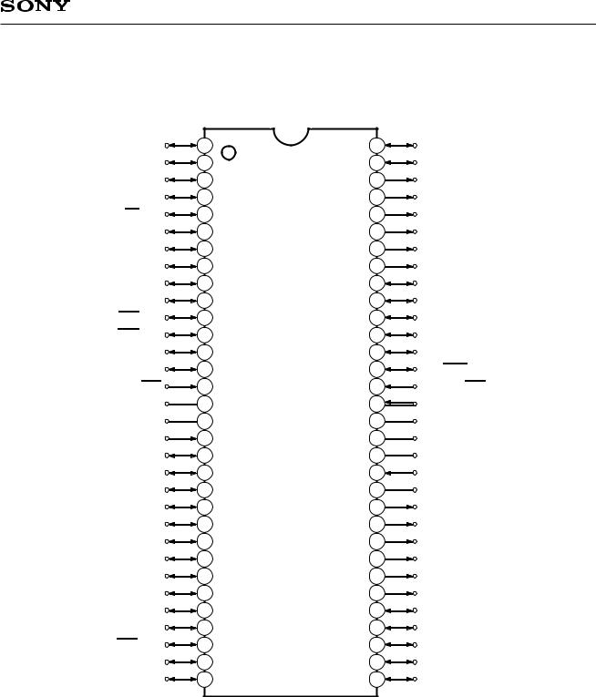
Pin Assignment (Top View) 64-pin SDIP
PC3 |
1 |
64 |
PC4 |
PC2 |
2 |
63 |
PC5 |
PC1 |
3 |
62 |
PC6/PWM6 |
PC0 |
4 |
61 |
PC7/PWM7 |
EC/PD7 |
5 |
60 |
PF0/PWM0 |
RMC/PD6 |
6 |
59 |
PF1/PWM1 |
HS1/PD5 |
7 |
58 |
PF2/PWM2 |
HS0/PD4 |
8 |
57 |
PF3/PWM3 |
SI/PD3 |
9 |
56 |
PF4/SCL0 |
SO/PD2 |
10 |
55 |
PF5/SCL1/PWM4 |
SCK/PD1 |
11 |
54 |
PF6/SDA0 |
INT2/PD0 |
12 |
53 |
PF7/SDA1/PWM5 |
HSYNC/PA7 |
13 |
52 |
PE0/TO/ADJ |
VSYNC/PA6 |
14 |
51 |
PE1/PWM |
RST |
15 |
50 |
PE2/TEX/INT0 |
VSS |
16 |
49 |
PE3/TX |
XTAL |
17 |
48 |
VSS |
EXTAL |
18 |
47 |
VDD |
PA5/AN5 |
19 |
46 |
NC |
PA4/AN4 |
20 |
45 |
EXLC |
PA3/AN3 |
21 |
44 |
XLC |
PA2/AN2 |
22 |
43 |
PE4/YM |
PA1/AN1 |
23 |
42 |
PE5/YS |
PA0/AN0 |
24 |
41 |
PE6/I |
PB7 |
25 |
40 |
B |
PB6 |
26 |
39 |
G |
PB5 |
27 |
38 |
R |
PB4 |
28 |
37 |
PB0 |
PB3 |
29 |
36 |
PB1 |
INT1/PG7 |
30 |
35 |
PB2 |
PG6 |
31 |
34 |
PG3 |
PG5 |
32 |
33 |
PG4 |
Note)
1.NC (Pin 46) is left open.
2.Vss (Pins 16 and 48) are both connected to GND.
–3 –
CXP750096/750010, CXP750097/750011
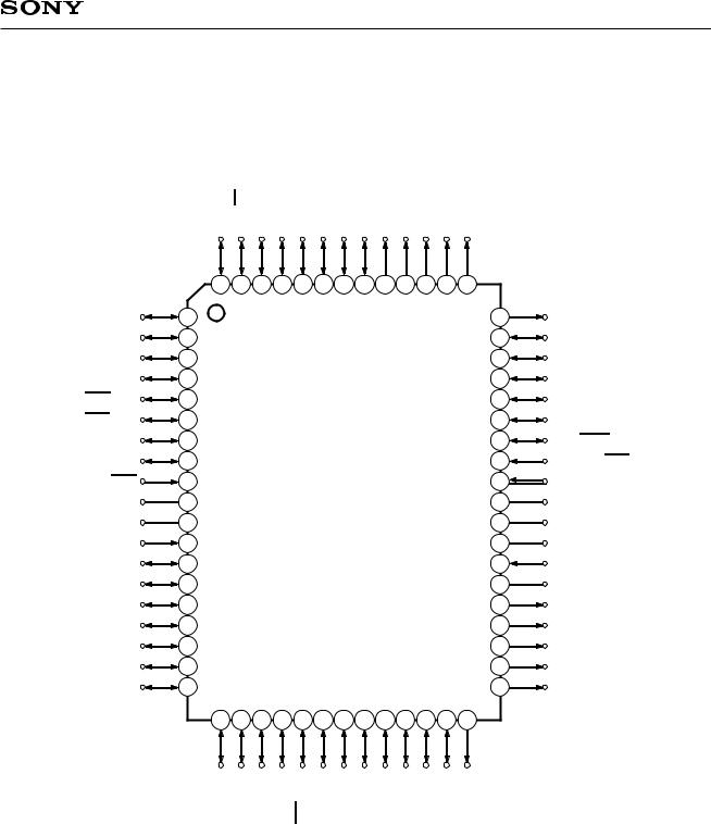
Pin Assignment (Top View) 64-pin QFP
|
CMR /6D P |
CE/ 7DP |
0CP |
1CP |
2CP |
3CP |
4CP |
5CP |
6MW P/6C P |
7MW P/7C P |
0MW P/0F P |
1MW P/1F P |
2MW P/2F P |
|
|
64 |
63 |
62 |
61 |
60 |
59 |
58 |
57 |
56 |
55 |
54 |
53 |
52 |
|
HS1/PD5 |
1 |
|
|
|
|
|
|
|
|
|
|
|
51 |
PF3/PWM3 |
HS0/PD4 |
2 |
|
|
|
|
|
|
|
|
|
|
|
50 |
PF4/SCL0 |
SI/PD3 |
3 |
|
|
|
|
|
|
|
|
|
|
|
49 |
PF5/SCL1/PWM4 |
SO/PD2 |
4 |
|
|
|
|
|
|
|
|
|
|
|
48 |
PF6/SDA0 |
SCK/PD1 |
5 |
|
|
|
|
|
|
|
|
|
|
|
47 |
PF7/SDA1/PWM5 |
INT2/PD0 |
6 |
|
|
|
|
|
|
|
|
|
|
|
46 |
PE0/TO/ADJ |
HSYNC/PA7 |
7 |
|
|
|
|
|
|
|
|
|
|
|
45 |
PE1/PWM |
VSYNC/PA6 |
8 |
|
|
|
|
|
|
|
|
|
|
|
44 |
PE2/TEX/INT0 |
RST |
9 |
|
|
|
|
|
|
|
|
|
|
|
43 |
PE3/TX |
VSS |
10 |
|
|
|
|
|
|
|
|
|
|
|
42 |
VSS |
XTAL |
11 |
|
|
|
|
|
|
|
|
|
|
|
41 |
VDD |
EXTAL |
12 |
|
|
|
|
|
|
|
|
|
|
|
40 |
NC |
PA5/AN5 |
13 |
|
|
|
|
|
|
|
|
|
|
|
39 |
EXLC |
PA4/AN4 |
14 |
|
|
|
|
|
|
|
|
|
|
|
38 |
XLC |
PA3/AN3 |
15 |
|
|
|
|
|
|
|
|
|
|
|
37 |
PE4/YM |
PA2/AN2 |
16 |
|
|
|
|
|
|
|
|
|
|
|
36 |
PE5/YS |
PA1/AN1 |
17 |
|
|
|
|
|
|
|
|
|
|
|
35 |
PE6/I |
PA0/AN0 |
18 |
|
|
|
|
|
|
|
|
|
|
|
34 |
B |
PB7 |
19 |
|
|
|
|
|
|
|
|
|
|
|
33 |
G |
|
20 |
21 |
22 |
23 |
24 |
25 |
26 |
27 |
28 |
29 30 |
31 |
32 |
|
|
|
6BP |
5BP |
4BP |
3BP |
7GP /1T NI |
6GP |
5GP |
4GP |
3GP |
2BP |
1BP |
0BP |
R |
|
Note)
1.NC (Pin 40) is left open.
2.Vss (Pins 10 and 42) are both connected to GND.
– 4 –
CXP750096/750010, CXP750097/750011
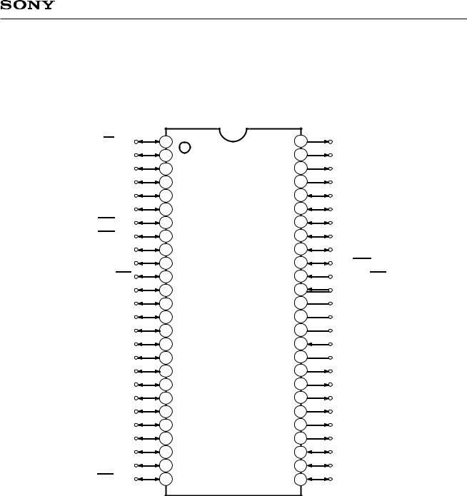
Pin Assignment (Top View) 52-pin SDIP
EC/PD7 |
1 |
52 |
PF0/PWM0 |
RMC/PD6 |
2 |
51 |
PF1/PWM1 |
HS1/PD5 |
3 |
50 |
PF2/PWM2 |
HS0/PD4 |
4 |
49 |
PF3/PWM3 |
SI/PD3 |
5 |
48 |
PF4/SCL0 |
SO/PD2 |
6 |
47 |
PF5/SCL1/PWM4 |
SCK/PD1 |
7 |
46 |
PF6/SDA0 |
INT2/PD0 |
8 |
45 |
PF7/SDA1/PWM5 |
HSYNC/PA7 |
9 |
44 |
PE0/TO/ADJ |
VSYNC/PA6 |
10 |
43 |
PE1/PWM |
RST |
11 |
42 |
PE2/TEX/INT0 |
VSS |
12 |
41 |
PE3/TX |
XTAL |
13 |
40 |
VSS |
EXTAL |
14 |
39 |
VDD |
PA5/AN5 |
15 |
38 |
NC |
PA4/AN4 |
16 |
37 |
EXLC |
PA3/AN3 |
17 |
36 |
XLC |
PA2/AN2 |
18 |
35 |
PE4/YM |
PA1/AN1 |
19 |
34 |
PE5/YS |
PA0/AN0 |
20 |
33 |
PE6/I |
PB7 |
21 |
32 |
B |
PB6 |
22 |
31 |
G |
PB5 |
23 |
30 |
R |
PB4 |
24 |
29 |
PB0 |
PB3 |
25 |
28 |
PB1 |
INT1/PG7 |
26 |
27 |
PB2 |
Note)
1.NC (Pin 38) is left open.
2.Vss (Pins 12 and 40) are both connected to GND.
–5 –

|
|
|
|
|
|
|
|
|
|
|
|
CXP750096/750010, CXP750097/750011 |
||
|
|
|
|
|
|
|
|
|
|
|
|
|
|
|
Pin Description |
|
|
|
|
|
|
|
|||||||
|
|
|
|
|
|
|
|
|
|
|
|
|
|
|
|
|
Symbol |
I/O |
|
|
|
Description |
|
||||||
|
|
|
|
|
|
|
|
|
|
|
|
|
|
|
PA0/AN0 |
I/O/ |
|
(Port A) |
Analog inputs to A/D converter. |
||||||||||
to |
|
|||||||||||||
Analog input |
|
8-bit I/O port. |
(6 pins) |
|
||||||||||
PA5/AN5 |
|
|
||||||||||||
|
|
I/O can be set in a |
|
|
|
|||||||||
|
|
|
|
|
|
|
|
|
|
|
|
|
||
PA6/VSYNC |
I/O/Input |
|
unit of single bits. |
OSD display vertical sync signal input. |
||||||||||
|
|
|
|
|
|
|
|
|
|
(8 pins) |
|
|
|
|
PA7/HSYNC |
I/O/Input |
|
OSD display horizontal sync signal input. |
|||||||||||
|
|
|
||||||||||||
|
|
|
|
|
|
|
|
|
|
|
|
|
|
|
|
|
|
|
|
|
|
|
|
|
(Port B) |
|
|
|
|
PB0 to PB7 |
I/O |
|
8-bit I/O port. I/O can be set in a unit of single bits. |
|||||||||||
|
|
|
|
|
|
|
|
|
|
(8 pins) |
|
|
|
|
|
|
|
|
|
|
|
|
|
|
|
|
|
|
|
|
|
|
|
|
|
|
|
|
|
(Port C) |
|
|
|
|
PC0 to PC5 |
I/O |
|
Lower 6 bits are I/O ports; I/O can be set in a unit of single bits. Upper |
|||||||||||
|
2 bits are output port and large current (12mA) N-channel open drain |
|||||||||||||
|
|
|
|
|
|
|
|
|
|
|||||
|
|
|
|
|
|
|
|
|
|
output. Upper 2 bits are medium drive voltage (12V); lower 6 bits are |
||||
|
|
|
|
|
|
|
|
|
|
5V drive. |
|
|
|
|
PC6/PWM6 to |
Output/Output |
|
(8 pins) |
8-bit PWM output. |
|
|||||||||
PC7/PWM7 |
|
|
|
(2 pins) |
|
|||||||||
|
|
|
|
|
|
|
|
|
|
|
|
External interruption request input. Active at the |
||
PD0/INT2 |
I/O/Input |
|
|
|
||||||||||
|
|
|
falling edge. |
|
||||||||||
|
|
|
|
|
|
|
|
|
|
|
|
|
||
|
|
|
|
|
|
|
|
|
|
|
|
|
|
|
|
|
|
|
I/O/I/O |
|
|
Serial clock I/O. |
|
||||||
PD1/SCK |
|
|
|
(Port D) |
|
|||||||||
PD2/SO |
I/O/Output |
|
8-bit I/O port. I/O |
Serial data output. |
|
|||||||||
|
can be set in a |
|
||||||||||||
|
|
|
|
|
|
|
|
|
|
|
|
|
||
PD3/SI |
I/O/Input |
|
Serial data input. |
|
||||||||||
|
unit of single bits. |
|
||||||||||||
PD4/HS0 |
I/O/Input |
|
Can drive 12mA |
HSYNC counter (CH0) input. |
||||||||||
|
synk current. |
|||||||||||||
|
|
|
|
|
|
|
|
|
|
|
|
|
||
PD5/HS1 |
I/O/Input |
|
HSYNC counter (CH1) input. |
|||||||||||
|
(8 pins) |
|||||||||||||
PD6/RMC |
I/O/Input |
|
|
|
Remote control reception circuit input. |
|||||||||
|
|
|
|
|
|
|
|
|
|
|
|
|
|
|
|
|
|
|
|
|
|
|
I/O/Input |
|
|
|
External event input for timer/counter. |
||
PD7/EC |
|
|
|
|
|
|
|
|
||||||
|
|
|
|
|
|
|
|
|
|
|
|
|
|
|
PE0/TO/ADJ |
I/O/Output/ |
|
|
|
Rectangular wave output |
|
TEX oscillation |
|||||||
Output |
|
|
|
for 8-bit timer/counter. |
|
frequency dividing output. |
||||||||
|
|
|
|
|
|
|
|
|
|
|
|
|||
|
|
|
|
|
|
|
|
|
|
|
|
|
|
|
|
|
|
I/O/Output |
|
|
|
14-bit PWM output. |
|
||||||
PE1/PWM |
|
|
(Port E) |
|
||||||||||
|
|
|
|
|
|
|
|
|
|
|
|
|
||
|
|
|
|
|
|
|
|
Input/Input/ |
|
Bits 0 and 1 are I/O |
Connects a crystal for |
|
External interruption |
|
PE2/TEX/INT0 |
|
port; I/O can be set |
|
request input. Active at |
||||||||||
Input |
|
32kHz timer/counter |
|
|||||||||||
|
|
|
|
|
|
|
|
|
in a unit of single. |
|
the falling edge. |
|||
|
|
|
|
|
|
|
|
|
|
clock oscillation. When |
|
|||
|
|
|
|
|
|
|
|
|
|
Bits 2 and 3 are |
|
|
||
|
|
|
|
|
|
|
|
|
|
used as an event |
|
|||
PE3/TX |
Input/Output |
|
input port. Bits 4, 5 |
|
||||||||||
|
counter, input to TEX pin and leave TX pin open. |
|||||||||||||
|
and 6 are output |
|||||||||||||
|
|
|
|
|
|
|
|
|
|
|
|
|
||
|
|
|
|
|
|
|
|
|
|
port. |
|
|
|
|
PE4/YM |
Output/Output |
|
|
|
|
|||||||||
|
(7 pins) |
|
|
|
||||||||||
|
|
|
|
|
|
|
|
|
|
|
|
|
||
PE5/YS |
Output/Output |
|
|
|
|
|
|
|||||||
|
|
|
|
|
|
|
|
|
|
|
|
|
|
|
PE6/I |
Output/Output |
|
|
|
OSD display 6-bit output. |
|
||||||||
|
|
|
|
|
|
|
|
|
|
|
|
|
||
B |
Output |
|
|
|
(6 pins) |
|
||||||||
|
|
|
|
|
|
|||||||||
|
|
|
|
|
|
|
|
|
|
|
|
|
|
|
G |
Output |
|
|
|
|
|
|
|||||||
|
|
|
|
|
|
|
|
|
|
|
|
|
|
|
R |
Output |
|
|
|
|
|
|
|||||||
|
|
|
|
|
|
|
|
|
|
|
|
|
|
|
Not incorporated for Pin 52 package. |
|
|
|
|
|
|||||||||
– 6 –

|
|
|
|
|
|
|
CXP750096/750010, CXP750097/750011 |
||
|
|
|
|
|
|
|
|
|
|
|
|
|
|
|
|
|
|
|
|
|
|
Symbol |
I/O |
|
Description |
||||
|
|
|
|
|
|
|
|
|
|
|
PF0/PWM0 to |
Output/Output |
(Port F) |
8-bit PWM output. |
|||||
|
PF3/PWM3 |
8-bit output port |
(4 pins) |
||||||
|
|
||||||||
|
|
|
|
|
|
and large current |
|
|
|
|
PF4/SCL0 |
Output/I/O |
I2C bus interface transfer clock I/O. |
||||||
|
(12mA) N-channel |
||||||||
|
|
|
|
|
|
(2 pins) |
|
||
|
PF5/SCL1/ |
Output/I/O/ |
open drain output. |
8-bit PWM output. |
|||||
|
|
|
|||||||
|
PWM4 |
Output |
Lower 4 bits are |
|
|
||||
|
|
|
|
||||||
|
|
|
|
|
|
medium drive |
|
|
|
|
PF6/SDA0 |
Output/I/O |
I2C bus interface transfer data I/O. |
||||||
|
voltage (12V); upper |
||||||||
|
|
|
|
|
|
(2 pins) |
|
|
|
|
PF7/SDA1/ |
Output/I/O/ |
|
|
|||||
|
4 bits are 5V drive. |
|
|
8-bit PWM output. |
|||||
|
PWM5 |
Output |
(8 pins) |
|
|
||||
|
|
|
|
||||||
|
|
|
|
|
|
|
|
|
|
|
PG3 to PG6 |
I/O |
(Port G) |
|
|
|
|||
|
|
|
|
|
|
5-bit I/O port. I/O can be set in a unit of single bits. |
|||
|
|
|
|
|
|
(5 pins) |
|
|
|
|
|
|
|
|
|
External interruption request input. |
|||
|
PG7/INT1 |
I/O/Input |
|
||||||
|
|
Active at the falling edge. |
|||||||
|
|
|
|
|
|
|
|||
|
|
|
|
|
|
|
|
|
|
|
EXTAL |
Input |
Connects a crystal for system clock oscillation. When a clock is |
||||||
|
|
|
|
|
|
supplied externally, input to EXTAL pin and input a reversed phase |
|||
|
XTAL |
Output |
|||||||
|
clock to XTAL pin. |
|
|
|
|||||
|
|
|
|
|
|
|
|
|
|
|
|
|
|
System reset; active at Low level. |
|||||
|
RST |
Input |
|||||||
|
|
|
|
|
|
|
|
|
|
|
EXLC |
Input |
OSD display clock oscillation I/O. Oscillation frequency is determined |
||||||
|
XLC |
Output |
by the external L and C. |
||||||
|
|
|
|
|
|||||
|
|
|
|
|
|
|
|
|
|
|
NC |
|
No connected. |
|
|
|
|||
|
|
|
|
|
|
|
|
|
|
|
VDD |
|
Positive power supply. |
||||||
|
|
|
|
|
|
|
|
|
|
|
Vss |
|
GND. Connect two Vss pins to GND. |
||||||
|
|
|
|
|
|
|
|
|
|
Not incorporated for Pin 52 package.
– 7 –
|
|
|
|
|
CXP750096/750010, CXP750097/750011 |
||
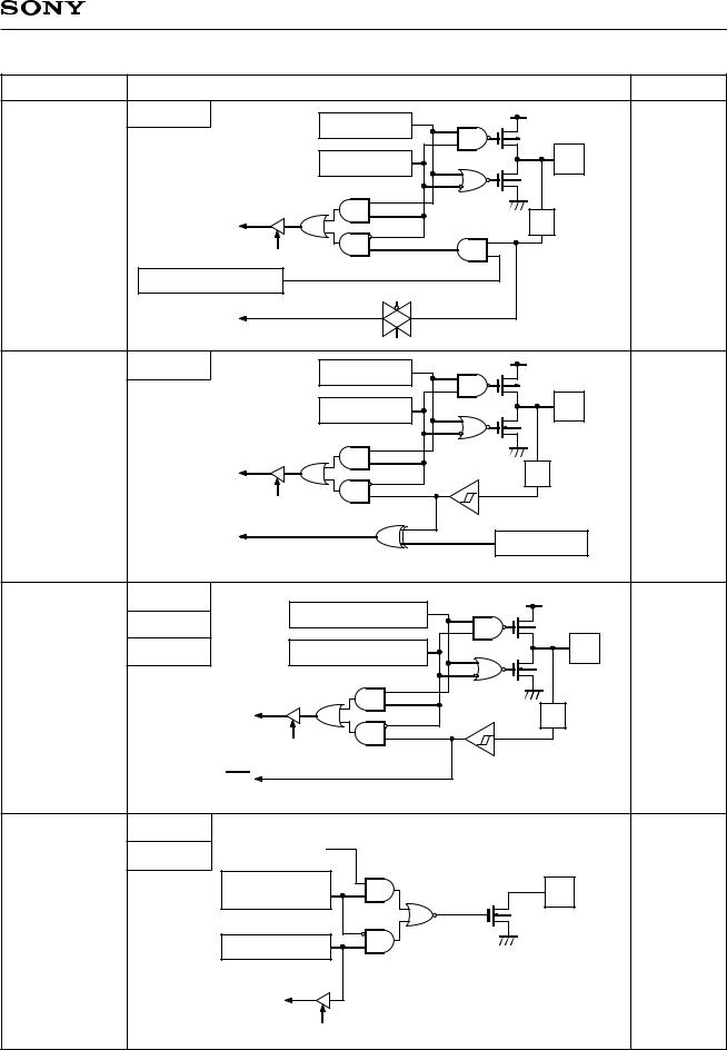
Input/Output Circuit Formats for Pins |
|
|
|
|
|
||
Pin |
|
|
Circuit format |
|
|
|
After a reset |
|
Port A |
|
Port A data |
|
|
|
|
|
|
|
|
|
|
|
|
|
|
|
Port A direction |
|
|
|
|
PA0/AN0 |
|
|
“0” after a reset |
|
|
|
|
to |
|
|
|
|
|
|
|
PA5/AN5 |
Internal data bus |
|
|
|
IP |
Hi-Z |
|
|
|
RD (Port A) |
|
|
Input |
|
|
|
|
|
|
protection |
|
||
|
|
|
|
|
|
|
|
|
Port A function selection |
|
|
|
circuit |
|
|
|
|
|
|
|
|
||
|
“0” after a reset |
Input multiplexer |
|
|
|
|
|
6 pins |
A/D converter |
|
|
|
|
||
|
|
|
|
|
|||
|
Port A |
|
Port A data |
|
|
|
|
|
|
|
|
|
|
|
|
|
|
|
Port A direction |
|
|
|
|
PA6/VSYNC |
|
|
“0” after a reset |
|
|
|
|
|
|
|
|
|
|
|
|
PA7/HSYNC |
|
|
|
Schmitt input |
|
|
Hi-Z |
|
Internal data bus |
|
|
IP |
|||
|
|
|
|
||||
|
|
RD (Port A) |
|
|
|
|
|
|
HSYNC, VSYNC |
|
|
Input polarity |
|
||
2 pins |
|
|
|
|
|
||
|
|
|
“0” after a reset |
|
|||
|
|
|
|
|
|||
|
Port B |
|
|
|
|
|
|
|
Port C |
|
Ports B, C, G data |
|
|
|
|
|
|
|
|
|
|
|
|
PB0 to PB7 2 |
Port G |
|
Ports B, C, G direction |
|
|
|
|
PC0 to PC5 |
|
|
“0” after a reset |
|
|
|
|
PG3 to PG6 2 |
|
|
|
|
|
|
|
|
|
|
|
|
|
Hi-Z |
|
PG7/INT1 |
|
|
|
PB0 to PB2 |
|
|
|
Internal data bus |
|
Schmitt input only |
IP |
|
|||
|
|
|
|||||
|
|
for PG7 |
|
|
|||
|
|
|
|
|
|
|
|
|
|
RD (Ports B, C, G) |
|
|
|
|
|
19 pins |
|
INT1 |
|
|
|
|
|
|
Port C |
PWM0 to PWM3 |
|
|
|
|
|
|
Port F |
|
|
|
|
||
PC6/PWM6 2 |
PWM6, PWM7 |
|
|
|
|
||
|
Ports C and F |
|
|
|
|
||
PC7/PWM7 2 |
|
|
|
|
|
||
|
function selection |
|
|
|
|
||
PF0/PWM0 |
|
“0” after a reset |
|
1 |
|
|
|
to |
|
|
|
|
Hi-Z |
||
|
|
|
|
|
|
||
PF3/PWM3 |
|
Ports C and F data |
|
|
|
||
|
|
|
|
|
|||
|
|
“1” after a reset |
1 12V drive voltage |
|
|||
|
|
|
|
|
Large current 12mA |
|
|
|
|
Internal data bus |
|
|
|
|
|
6 pins |
|
|
RD (Ports C, F) |
|
|
|
|
|
|
|
|
|
|
|
|
2 Not incorporated for Pin 52 package.
– 8 –
 Loading...