


 Loading...
CDP-XE510
SERVICE MANUAL
AEP Model
UK Model
Photo: BLACK
Model Name Using Similar Mechanism |
CDP-XE500 |
|
|
CD Mechanism Type |
CDM14-5BD22 |
|
|
Base Unit Type |
BU-5BD22 |
|
|
Optical Pick-up Type |
KSS-213BA/F-NP |
|
|
SPECIFICATIONS
COMPACT DISC PLAYER
MICROFILM
— 1 —
The laser component in this product is capable of emitting radiation exceeding the limit for Class 1.
This appliance is classified as a CLASS 1 LASER product. The CLASS 1 LASER PRODUCT MARKING is located on the rear exterior.
This caution label is located inside the unit.
CAUTION
Use of controls or adjustments or performance of procedures other than those specified herein may result in hazardous radiation exposure.
Notes on chip component replacement
•Never reuse a disconnected chip component.
•Notice that the minus side of a tantalum capacitor may be damaged by heat.
Flexible Circuit Board Repairing
•Keep the temperature of soldering iron around 270˚C during repairing.
•Do not touch the soldering iron on the same conductor of the circuit board (within 3 times).
•Be careful not to apply force on the conductor when soldering or unsoldering.
SAFETY-RELATED COMPONENT WARNING !!
COMPONENTS IDENTIFIED BY MARK !OR DOTTED LINE WITH MARK !ON THE SCHEMATIC DIAGRAMS AND IN
THE PARTS LIST ARE CRITICAL TO SAFE OPERATION. REPLACE THESE COMPONENTS WITH SONY PARTS WHOSE PART NUMBERS APPEAR AS SHOWN IN THIS MANUAL OR IN SUPPLEMENTS PUBLISHED BY SONY.
TABLE OF CONTENTS |
|
1. SERVICING NOTE .......................................................... |
3 |
2. GENERAL .......................................................................... |
4 |
3. DISASSEMBLY |
|
3-1. Front Panel ........................................................................... |
5 |
3-2. Base Unit (BU-5BD22) ......................................................... |
5 |
4. TEST MODE ....................................................................... |
6 |
5. ELECTRICAL BLOCK CHECKING .......................... |
8 |
6. DIAGRAMS |
|
6-1. IC Block Diagrams ............................................................. |
10 |
6-2. Circuit Boards Location ...................................................... |
13 |
6-3. Printed Wiring Board — BD Section — ............................. |
15 |
6-4. Schematic Diagram — BD Section — ............................... |
17 |
6-5. Printed Wiring Board — Main Section — .......................... |
19 |
6-6. Schematic Diagram — Main Section — ............................ |
21 |
6-7. Printed Wiring Board — Panel Section — ......................... |
23 |
6-8. Schematic Diagram — Panel Section — ............................ |
25 |
6-9. Printed Wiring Board — Loading, HP Section — .............. |
27 |
6-10. Schematic Diagram — Loading, HP Section — .............. |
28 |
6-11. IC Pin Functions ............................................................... |
29 |
7. EXPLODED VIEWS |
|
7-1. Main Section ....................................................................... |
33 |
7-2. Mechanism Deck Section (CDM14-5BD22) ...................... |
34 |
7-3. Base Unit Section (BU-5BD22) .......................................... |
35 |
8. ELECTRICAL PARTS LIST ........................................ |
36 |
MODEL IDENTIFICATION |
|
– BACK PANEL – |
|
|
Parts No. |
|
|
MODEL |
PARTS No. |
|
|
AEP, EE, CIS |
4-987-946-0 |
|
|
UK |
4-987-946-1 |
|
|
•Abbreviation
EE : East European model
— 2 —
SECTION 1
SERVICING NOTE
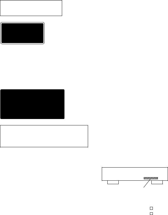
HOW TO OPEN THE DISC TRAY WHEN POWER SWITCH TURNS OFF
Insert a tapering driver into the aperture of the unit bottom, and turn in the direction of arrow.
* To close the disc table, turn the driver in the reverse direction.
CD-TEXTTEST DISC
This unit is able to display the text data (character information) written in the CD on its fluorescent indicator tube.
The CD-TEXT TEST DISC (TGCS-313: J-2501-126-A) is used for checking the display.
To check, perform the following procedure.
Procedure:
1.Turn ON the power and set the test disc.
2.Press the ” button and play back the disc.
3.The following will be displayed on the fluorescent indicator tube. Display : 1kHz/0 dB/ L&R
4.Rotate the AMS ± knob to switch the track. The text data of each track will be displayed.
Restrictions in CD-TEXT Contents and Display
The micro processor’s RAM has limit of capacity in this unit, The display may not show all the track titles in a disc when you play the CD TEXT TEST DISC, but it is not unusual. In that case, “NOT DISPLAY” appears in the display.
Pull out disc table
NOTES ON HANDLINGTHE OPTICAL PICK-UP BLOCK OR BASE UNIT
The laser diode in the optical pick-up block may suffer electrostatic breakdown because of the potential difference generated by the charged electrostatic load, etc. on clothing and the human body.
During repair, pay attention to electrostatic breakdown and also use the procedure in the printed matter which is included in the repair parts.
The flexible board is easily damaged and should be handled with care.
NOTES ON LASER DIODE EMISSION CHECK
The laser beam on this model is concentrated so as to be focused on the disc reflective surface by the objective lens in the optical pick-up block. Therefore, when checking the laser diode emission, observe from more than 30 cm away from the objective lens.
LASER DIODE AND FOCUS SEARCH OPERATION CHECK
Carry out the “S curve check” in “CD section adjustment” and check that the S curve waveform is output two times.
— 3 —
SECTION 2
GENERAL
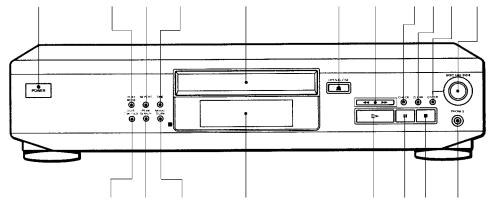
LOCATION OF PARTS AND CONTROLS
Front Panel
1 |
2 |
3 |
4 |
5 |
6 |
7 |
890 !¡ |
!ª !• !¶ |
!§ |
! !¢ !£ !™ |
1 POWER switch |
|
!¡ AMS* ±knob |
2 PLAY MODE button |
|
!™ PHONES jack |
3 REPEAT button |
|
!£ p(stop) button |
4 TIME button |
|
!¢ P(pause) button |
5 Disc tray |
|
! ·(play) button |
6 §OPEN/CLOSE button |
|
!§ Display window |
7 0/)buttons |
|
!¶ MUSIC SCAN button |
8 CHECK button |
|
!• PEAK SEARCH button |
9 CLEAR button |
|
!ª EDIT/TIME FADE button |
!º ENTER button |
|
|
|
|
* AMS is the abbreviation for Automatic Music Sensor. |
— 4 —
SECTION 3
DISASSEMBLY
Note : Follow the disassembly procedure in the numerical order given.
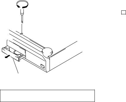
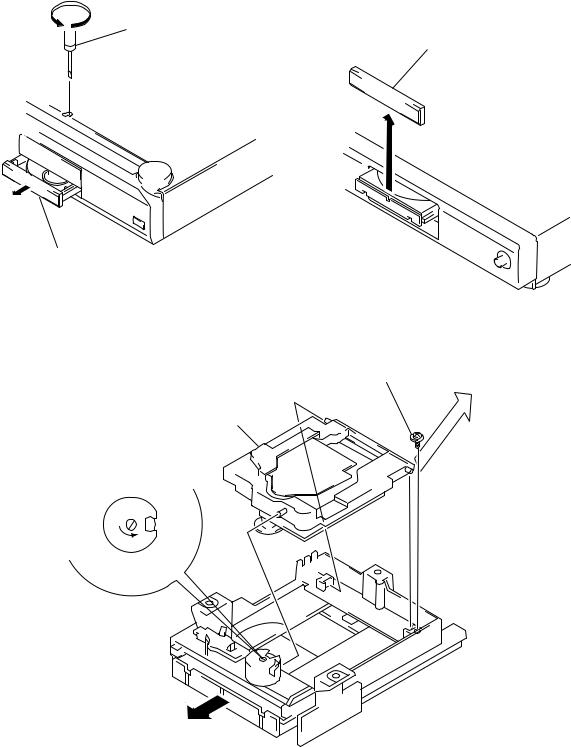
3-1. FRONT PANEL
• In order to remove the front panel block when the power supply does not turn on, rotate the cam with tapering driver as the figure shows, and the loading part will be moved.
Then pull out the loading part by your hand to remove the loading panel as the figure shows. After that take out the front panel block.
Tapering driver
Loading panel
Loading part
3-2. BASE UNIT (BU-5BD22)
3 Yoke bracket
BU-5BD22
1 Turn the cam to the direction of arrow (counter clock wise)
by tapering driver.
4Remove the Base unit (BU-5BD22) to the direction of arrow.
2 Take off the disc table.
— 5 —
SECTION 4 TEST MODE
4-1. AF MODE
The following checks can be performed in the AF mode, which is set by connecting the TP2 (AFADJ) terminal on MAIN board to the Ground and turning on the power.
• FL tube check
After all segments light up, when the · button is pressed, the following will be displayed. (Partial lighting 1)
A B C D E F
(Partial lighting 1)
When the p button is pressed, the following will be displayed. (partial lighting 2)
(Partial lighting 2)
The display will light up as follows (partial lighting 3) when theAMS ±knob is rotated to the right, and as follows (partial lighting 4) when rotated to the left.
Button |
Button No. |
|
Button |
Button No. |
Displayed |
|
Displayed |
||
|
|
|
||
|
|
|
|
|
CHECK |
0 |
|
PLAY MODE |
12 |
|
|
|
|
|
) |
1 |
|
REPEAT |
13 |
|
|
|
|
|
0 |
2 |
|
TIME |
14 |
|
|
|
|
|
P |
4 |
|
OPEN/ |
All lit |
|
|
|
CLOSE § |
|
ENTER |
6 |
|
||
|
|
|||
|
|
|
|
|
CLEAR |
7 |
|
PLAY · |
Partial lighting 1 |
|
|
|
|
|
MUSIC SCAN |
9 |
|
STOP p |
Partial lighting 2 |
|
|
|
|
|
PEAK SEARCH |
10 |
|
|
|
|
|
|
|
|
EDIT/ |
11 |
|
|
|
TIME FADE |
|
|
|
|
|
|
|
|
|
|
|
|
|
|
• Remote commander check
When buttons other than the · button are pressed when the whole display is lit, the display will change to partial lighting 2. When the “ ·” button is pressed, the display will light up as follows.
REMOCON PLAY
(Partial lighting 5)
JOG RIGHT
(Partial lighting 3)
JOG LEFT
(Partial lighting 4)
When the OPEN/CLOSE § button is pressed, all will light up again.
• Key check
All buttons have corresponding button numbers. When a button is pressed, the counter will count up and display the button’s number. However, the counter will only count to “15”. It will not count for buttons already pressed once, but will display the button’s number.
88 TOTAL= 88
ÂÂ
Display of button number |
Display of counting |
— 6 —

4-2. ADJ MODE
The following operations are performed in the ADJ mode, which is set by connecting the TP1 (ADJ) terminal to the Ground and turning on the power.
•During playback, there is no problem even if the GFS is continuously LOW.
•High speed search is prohibited during access.
•During playback, the gain of focus servo and spindle servo does not decrease.
•Servo related manual operations and measurement can be performed.
(For details of operations, refer to Table of Button Operrations in ADJ Mode.)
Table of Button Operations in ADJ Mode
The jitter value display mode can be set after the all-music remaining number mode using the TIME button.
The functions of the number buttons are shown in the following table.
Function of Number Buttons
(With the Attached Remote Commander)
Button |
Function |
1 |
Focus bias 8-step up |
|
|
2 |
Middle of focus bias up/down turning point |
|
|
3 |
Tracking servo, sled servo off |
|
|
4 |
Auto gain initialization |
|
|
5 |
Focus servo off |
|
|
6 |
Focus bias 8-step down |
|
|
7 |
Immediate readjustment of focus bias |
|
|
8 |
Tracking servo, sled servo on |
|
|
10 |
Auto focus bias start point |
|
|
4-3. CLV-S MODE
The spindle servo for playback sets into the CLV-S mode when the TP2 (AFADJ) terminal is connected to Ground after turning on the power.
[ MAIN BOARD ] — Component Side —
IC631
CN621
TP2 (AFADJ)
R622
TP1 (ADJ)
R621
IC621
— 7 —
SECTION 5
ELECTRICAL BLOCK CHECKING
Note:
1.CD Block is basically designed to operate without adjustment. Therefore, check each item in order given.
2.Use YEDS-18 disc (3-702-101-01) unless otherwise indicated.
3.Use an oscilloscope with more than 10MW impedance.
4.Clean the object lens by an applicator with neutral detergent when the signal level is low than specified value with the following checks.
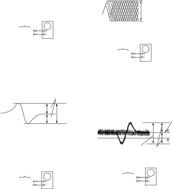
S Curve Check
oscilloscope
BD board
TP (FE)
TP (VC)
Procedure :
1.Connect oscilloscope to test point TP (FE) on BD board.
2.Connect between test point TP (FEI) and TP (VC) by lead wire.
3.Turn Power switch on.
4.Put disc (YEDS-18) in and turn Power switch on again and actuate the focus search. (actuate the focus search when disc table is moving in and out.)
5.Check the oscilloscope waveform (S-curve) is symmetrical between A and B. And confirm peak to peak level within 3±1 Vp-p.
S-curve waveform
symmetry
A
within 3 ± 1 Vp-p
B
6. After check, remove the lead wire connected in step 2.
Note :
•Try to measure several times to make sure than the ratio of A : B or B : A is more than 10 : 7.
•Take sweep time as long as possible and light up the brightness to obtain best waveform.
RF Level Check
oscilloscope
BD board
TP (RF)
TP (VC)
Procedure :
1.Connect oscilloscope to test point TP (RF) on BD board.
2.Turn Power switch on.
3.Put disc (YEDS-18) in to play the number five track.
4.Confirm that oscilloscope waveform is clear and check RF signal level is correct or not.
Note:
A clear RF signal waveform means that the shape “ à” can be clearly distinguished at the center of the waveform.
RF signal waveform
VOLT/DIV : 200mV
TIME/DIV : 500ns
level : 1.25 ± 0.25 Vp-p
E-F Balance (1 Track Jump) Check (Without remote commander)
oscilloscope
BD board
TP (TE)
TP (VC)
Procedure :
1. Connect oscilloscpe to test point TP (TE) on BD board. 2. Turn Power switch on.
3. Put disc (YEDS-18) in to play the number five track.
4. Press the “ P(Pause)” button. (Becomes the 1 track jump mode) 5. Check the level B of the oscilliscope's waveform and the A (DC
voltage) of the center of the Traverse waveform. Confirm the following :
A/B x 100 = less than ± 22%
1 track jump waveform
Center of the waveform
B
A (DC voltage)
0V
level : 1.3 ± 0.6 Vp-p
symmetry
E-F Balance Check (With remote commander)
oscilloscope
BD board
TP (TE)
TP (VC)
Procedure :
1.Connect the test point TP1 (ADJ) on MAIN board to the ground with a lead wire on main board.
2.Connect oscilloscpe to test point TP (TE) on BD board.
3.Turn the Power switch on to set the ADJ mode.
4.Put disc (YEDS-18) in to play the number five track.
5.Press the “3” button. (The tracking servo and the sledding servo are turned OFF.)
— 8 —
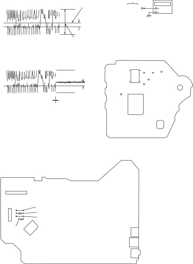
6.Check the level B of the oscilliscope's waveform and the A (DC voltage) of the center of the Traverse waveform.
Confirm the following : A/B x 100 = less than ± 22%
Traverse waveform
Center of the waveform
B
A (DC voltage) 0V 
level : 1.3 ± 0.6 Vp-p
RF PLL Free-run Frequency Check
Procedure :
1. Connect frequency counter to test point (PLCK) with lead wire.
frequency counter
BD board
TP (PLCK)
2.Turn Power switch on.
3.Put the disc (YEDS-18) in to play the number five track. Confirm that reading on frequency counter is 4.3218MHz.
7.Press the “8” button. (The tracking servo and sledding servo are turned ON.) Confirm the C (DC voltage) is almost equal to the A (DC voltage) is step 6.
Traverse waveform
|
C (DC |
0V |
voltage) |
Tracking servo |
Tracking servo |
Sledding servo |
Sledding servo |
OFF |
ON |
8. Disconnect the lead wire of TP1 (ADJ) connected in step 1.
[ MAIN BOARD ] — Component Side —
IC631
CN621 |
TP2 (AFADJ) |
R622
TP1 (ADJ)
R621
IC621
Adjustment Location :
[ BD BOARD ] — Side A —
1 |
20 |
(FE) |
|
|
(FEI) |
IC103 |
(RF) |
|
|
|
(TE) |
10 |
11 |
|
|
(VC) |
|
(PLCK)
IC101
J621
J681
IC651
— 9 —

SECTION 6
DIAGRAMS
6-1. IC BLOCK DIAGRAMS
IC101 CXD2545Q |
|
|
|
|
|
|
|
|
|
|
|
|
|
|
|
||||
|
|
|
|
FSTO XTAI |
XTAO XTSL |
VCKI VPCO |
|
|
|
|
|
|
|
|
|
|
|
|
|
|
|
|
67 62 63 64 |
20 19 |
|
|
|
|
|
|
|
|
|
|
|
|
|||
|
|
|
|
|
|
|
|
|
|
|
|
32K RAM |
|
|
|
|
|
|
|
C4M |
68 |
|
|
CLOCK |
|
|
|
|
|
|
|
|
|
|
|
|
|
|
|
C16M |
69 |
|
|
GENERATOR |
|
|
|
|
|
|
|
|
|
|
|
43 |
PSSL |
||
PDO |
18 |
|
|
|
|
|
|
|
|
RESISTER |
|
|
|
|
|
|
|
|
|
VCO1 |
13 |
|
|
DIGITAL |
|
EFM |
|
ADDRESS |
PRIORITY |
SERIAL |
|
|
|
|
|
||||
VCO0 |
12 |
|
|
PLL |
|
|
GENERATOR |
ENCODER |
|
|
|
|
|
|
|||||
|
|
VARI-PITCH |
|
DEMODULATOR |
|
|
|
PARALLEL |
|
16 |
61-46 DA01-16 |
||||||||
PCO |
33 |
|
(DOUBLE SPEED) |
|
|
|
|
|
PROCESSOR |
|
|
||||||||
|
|
|
|
|
|
|
|
|
|
|
|||||||||
FILI |
32 |
|
|
|
|
|
|
|
|
|
|
|
|
|
|
|
|
|
|
FILO |
31 |
|
|
|
|
|
SYNC |
|
|
|
D/A |
|
|
|
|
79 |
MUTE |
||
CLTV |
34 |
|
|
|
|
|
|
|
|
|
|
|
|
|
|
|
|||
|
|
|
|
|
PROTECTOR |
|
|
|
DATA PROCESSOR |
|
|
|
|
|
|
||||
RFAC |
36 |
ASYMMETRY |
|
|
|
|
|
|
|
|
|
|
|
|
|
|
|
||
ASYI |
38 |
|
MUX |
|
|
|
|
|
|
PEAK DETECTOR |
|
|
|
|
|
||||
CORRECTION |
|
|
|
|
|
|
|
|
|
|
|
|
|||||||
ASYO |
39 |
|
|
|
|
|
|
|
|
|
|
|
|
|
|
|
|||
|
|
|
|
|
|
|
|
|
|
|
|
|
|
|
|
|
|
||
ASYE |
42 |
|
|
|
|
|
|
|
|
|
|
|
DIGITAL OUT |
|
|
|
71 |
D OUT |
|
WFCK |
73 |
|
|
|
|
TIMING |
|
|
|
|
|
|
|
|
|
|
|
|
|
SCOR |
74 |
|
|
|
|
GENERATOR 1 |
|
|
|
|
|
|
|
|
|
70 |
MD2 |
||
EXCK |
76 |
|
|
|
|
SUBCODE |
|
|
ERROR CORRECTOR |
|
|
|
|
|
|
|
|||
SBSO |
75 |
|
|
|
|
P-W |
|
|
|
|
|
|
|
|
|
|
|
|
|
EMPH |
72 |
|
|
|
PROCESSOR |
|
|
|
|
|
|
|
|
|
86 |
DATA |
|||
|
|
|
|
SUBCODE |
|
|
|
|
|
|
|
|
|
||||||
SQCK |
78 |
|
|
|
|
|
|
|
|
|
CPU INTERFACE |
|
|
88 |
CLOK |
||||
SQSO |
77 |
|
|
|
|
Q |
|
|
|
|
|
|
|
|
|
|
87 |
XLAT |
|
|
|
|
PROCESSOR |
|
|
|
|
|
|
|
|
|
|||||||
MON |
95 |
|
|
|
|
|
|
CLV |
|
|
|
|
|
|
|
|
|
|
|
FSW |
94 |
|
|
|
|
|
|
|
|
|
|
|
|
|
|
|
|
|
|
MDP |
96 |
|
|
|
|
|
|
PROCESSOR |
|
|
SERVO |
|
|
|
|
|
|
||
|
|
|
|
|
|
|
|
|
TIMING |
|
|
|
80 |
SENS |
|||||
MDS |
97 |
|
|
|
|
|
|
|
|
|
AUTO |
|
|
|
|||||
|
|
|
18-TIMES |
|
|
|
GENERATOR 2 |
|
|
|
|||||||||
|
|
|
NOISE |
|
|
|
|
|
SEQUENCER |
|
|
|
|
|
|
||||
|
|
|
OVERSAMPLING |
|
|
|
SERVO |
|
|
|
|
|
|
|
|
||||
|
|
|
SHAPER |
|
|
|
|
|
|
|
|
|
|
|
|||||
|
|
|
|
FILTER |
|
|
|
MICRO PROGRAM |
|
|
|
|
|
|
|
||||
|
|
|
|
|
|
|
|
|
|
|
|
|
89 |
COUT |
|||||
|
|
|
|
|
|
|
|
|
|
|
INTERFACE |
|
|
|
|
||||
|
|
|
|
|
|
|
|
MIRR |
|
|
|
|
|
|
|
|
91 |
MIRR |
|
|
|
|
|
|
|
|
|
DFCT |
|
|
|
|
|
|
|
|
92 |
DFCT |
|
|
|
|
|
|
|
|
FOK DETECTOR |
|
|
|
|
|
|
|
|
93 |
FOK |
||
RFDC |
26 |
|
|
|
|
|
|
|
|
|
SERVO DSP |
PWM GENERATOR |
|
|
|
|
|
||
TE |
27 |
SWITCH |
|
|
|
|
|
|
|
2 |
|
|
|
|
|||||
|
A/D |
|
|
|
|
|
|
|
SLED PWM |
|
|
3, 100 |
SFON, SFDR |
||||||
SE |
28 |
|
|
|
|
|
|
SLED SERVO |
|
2 |
|
||||||||
|
& |
CONVERTER |
|
|
|
|
GENERATOR |
|
|
1, 2 |
|
SRON, SRDR |
|||||||
FE |
29 |
BUFFER |
|
|
|
|
|
|
|
2 |
|
|
|||||||
|
|
|
|
|
|
|
|
|
TRACKING |
TRACKING PWM |
|
4, 7 |
|
TFDR, TFON |
|||||
VC |
30 |
|
|
|
|
|
|
|
|
|
2 |
|
|
||||||
|
|
|
|
|
|
|
|
|
SERVO |
|
GENERATOR |
|
|
5, 6 |
|
TRON, TRDR |
|||
|
|
|
|
|
|
|
|
|
|
|
|
|
2 |
|
|
||||
|
|
|
|
|
|
|
|
|
|
|
|
|
FOCUS PWM |
|
|
8, 11 |
|
FFDR, FFON |
|
|
|
|
|
|
|
|
|
|
|
|
FOCUS SERVO |
|
2 |
|
|
||||
|
|
|
|
|
|
|
|
|
|
|
GENERATOR |
|
|
9, 10 |
|
FRON, FRDR |
|||
|
|
|
|
|
|
|
|
|
|
|
|
|
|
|
|
|
|||
|
|
25 24 |
14 16 17 |
21 40 23 35 |
41 90 15 65 |
81 |
22 37 44 45 66 82 83 84 85 98 99 |
|
|
|
|
|
|||||||
|
|
RFC |
ADIO |
TEST TES2 |
TES3 |
AVDD |
AVDD AVSS AVSS |
ADD ADD |
DVSS |
DVSS |
XRST |
IGEN BIAS WDCK |
LRCK FSTI DIRC SCLK DFSW |
ATSK LOCK SSTP |
|
|
|
|
|
|
|
IC102 BA6392FP-T1 |
|
|
|
|
|
|
|
|
|
|
|
|
|||||
CH1 OUT F |
1 |
BUFF |
|
28 |
GND |
F |
|
||||
|
|
|
|
|
|
CH1 OUT R |
2 |
BUFF |
BUFF |
27 |
CH4 OUT F |
|
LEVEL |
||||
|
|
R |
|
|
|
|
|
SHIFT |
|
|
|
CAPA IN 1 |
3 |
|
26 |
CH4 OUT R |
|
|
BUFF |
||||
|
|
R |
|
|
|
CH1 R IN |
4 |
|
25 |
VB IN |
|
|
|
INTERFACE |
|
|
|
CH1 F IN |
5 |
F |
|
24 |
VS IN |
|
|
BUFF |
|
|
|
VREF IN |
6 |
|
|
23 |
VB IN |
VREF OUT |
7 |
|
|
22 |
VCC |
GND |
8 |
|
|
21 |
VCC |
CH2 F IN |
9 |
F |
F |
20 |
CH3 F IN |
|
|
INTERFACE |
INTERFACE |
|
|
CH2 R IN |
10 R |
R 19 |
CH3 R IN |
||
CAPA IN 2 |
11 |
R |
F |
18 |
CAPA IN 3 |
|
|
|
|
||
CH2 OUT R |
12 |
BUFF |
BUFF |
17 |
CH3 OUT R |
|
|
||||
|
|
F |
R |
|
|
CH2 OUT F |
13 |
BUFF |
BUFF |
16 |
CH3 OUT F |
|
|
||||
|
|
|
MUTE |
|
|
GND |
14 |
|
|
15 |
MUTE |
— 10 —
Loading...