


Order No. ITD1212911GE
Model No. PDP-2012
PDP-2011
PDP-2010
Hints for SC/SN Board Repair ( PDP 2012 - 2010 model )
Issue date : Dec. 2012
c Panasonic Corporation 2012
Unauthorized copying and distribution is
a violation of law.
1

< Caution >
1. (HD model = X/C/A series only)
Before checking the SN board with the TV set, check all key components with multi meter.
 Depending on the defective area of SN board,
SSboard damage may occur.
2.All key components must be checked and
all defective components must be replaced at the same time.
 If some defective components remain,
other components may become damaged again.
3. When assembling the SN/SC board to the TV set, the screws must be properly fastened.
 If screws are loosely tightened, there is a possibility of shutdown or board damage.
2

Contents
1.Block Diagram ( Difference of ’10/’11/’12 )
< 2012 model >
2-1.Explanation of Scan Board Operation and Check Point
2-2.Check List
2-3.Repair Data
< 2011 model >
3-1.Explanation of Scan Board Operation and Check Point
3-2.Check List
3-3.Repair Data
< 2010 model >
4-1.Explanation of Scan Board Operation and Check Point
4-2.Check List
4-3.Repair Data
3

1.Block Diagram ( Difference of ’10/’11/’12 )
4
Panel drive ( 2012/2011 Full-HD model (except 42inch) )
P board
VSUS |
VSUS |
VSUS |
SC |
|
|
|
SC |
Vscn Gen.
VFO |
SU |
SU |
VFG |
VOL |
|
Vad Gen. |
SD |
VSUS |
SD |
PDP panel
P board
SS |
VSUS |
VSUS |
|
|
|
SS |
|
Ve Gen. |
|
|
PDP panel
< 2012 model > |
T*-P42GT50/ST50* |
:TNPA5523** |
|
|
|
T*-P42UT50* |
:TNPA5620** |
|
|
< 2011 model > |
T*-P42 |
ST30/UT30/S30/U30* : TNPA5349** |
|
|
|
T*-P42 |
VT30/GT30* |
: TNPA5330** |
5 |
|
T*-P42 |
G30 |
: TNPA5457** |
|

Panel drive ( 2012/2011 42inch Full-HD model )
P board
|
|
|
VSUS |
|
VSUS |
|
VSUS |
SN |
|
|
|
|
|
|
|
|
SN |
|
|
|
|
|
|
|
|
Vscn Gen.
VFO
VFG |
VOL |
Vad Gen.
VSUS
PDP panel
< 2012 model > T*-P42GT50/ST50* |
:TNPA5523** |
|
T*-P42UT50* |
:TNPA5620** |
|
< 2011 model > T*-P42 |
ST30/UT30/S30/U30* : TNPA5349** |
|
T*-P42 |
VT30/GT30* |
: TNPA5330** |
T*-P42 |
G30 |
: TNPA5457** |
P board
SS |
VSUS |
VSUS |
|
|
|
SS |
|
Ve Gen. |
|
|
PDP panel
6
Panel drive ( 2012/2011 HD model )
P board |
P board |
|
VSUS |
VSUS VSUS |
SN |
SS |
VSUS |
VSUS |
Vscn Gen. |
|
SN |
|
|
|
|
|
SS |
|
Ve Gen. |
|
|
|
|
|
|
|
VFO |
|
|
|
|
|
VFG |
VOL |
|
MID |
|
|
Vad Gen. |
|
( only 2011 ) |
|
|
|
|
|
|
|
|
|
VSUS |
|
|
|
|
PDP panel |
PDP panel
< 2012 model > |
T*-P42X5/X50/C5/C50*, TC-P46X5* :TNPA5592** |
|
|
T*-P50X5/X50/C5/C50* |
:TNPA5593** |
< 2011 model > |
T*-P42X3/X30/C3/C30*, TC-P46X3* : TNPA5311** |
|
|
T*-P50X3/X30/C3/C30* |
: TNPA5312** |
7
Panel drive ( 2010 Full-HD model )
P board
SM board (only 42inch)
VSUS |
VSUS |
VSUS |
SC |
|
|
|
SC |
Vscn Gen.
VFO |
SU |
SU |
|
VFG |
|
VOL |
|
Vad Gen. |
SD |
|
SD |
VSUS |
|
PDP panel
T*-P42/46/50/55 VT20/VT25/GT20/GT25/V20/G20/G25/S20/S2* : TNPA5081**
T*-P42/46/50 |
S20/S25/S2/U20/U2* |
: TNPA5105** |
T*-P58/65 |
VT20/VT25/S20/S2* |
: TNPA5175** |
P board
SS |
VSUS |
VSUS |
|
|
|
SS |
|
Ve Gen. |
|
|
PDP panel
8

Panel drive ( 2010 50/37inch HD model )
SU |
SU |
SD |
SD |
PDP panel
P board
VSUS |
|
VSUS |
|
VSUS |
|
|
|
|
|
Vscn Gen.
VFO |
VFG
VOL
Vad Gen.
VSUS
|
|
P board |
|
SC |
SS |
VSUS |
VSUS |
SC |
SS |
||
|
|
Ve Gen. |
|
|
|
|
|
SC3 |
SS3 |
|
|
|
MID |
|
|
PDP panel
T*-P50 C2/X2/X20* |
: TNPA5063** |
TX-P37 C2/X20/X25* |
: TNPA5062** |
9

Panel drive ( 2010 42/46inch HD model )
P board
|
|
VSUS |
|
VSUS |
|
VSUS |
|
|
|
|
|
|
|
|
|
|
|
|
|
|
Vscn Gen.
VFO |
VFG
VOL
Vad Gen.
VSUS
PDP panel
|
|
P board |
|
SN |
SS |
VSUS |
VSUS |
SN |
SS |
||
|
|
Ve Gen. |
|
|
|
|
|
SN3 |
SS3 |
|
|
|
MID |
|
|
PDP panel
T*-P42X2/X20/C2/C20/A20*, TC-P46C2* : TNPA5066**
10
< 2012 model >
2-1.Explanation of Scan Board Operation
and Check Point
11

Check Flow of SC/SN Board Repair |
< 2012 model > |
|
|
Before power-on for checking, replace all defective components in BLOCK 1, 2 and 3.
Block1.
Check of IGBT/Tr (C-E),
FET (S-D) and Diode
All OK
Block2.
Check of Scan Drive IC
(Only SN board)
All OK
Block3.
Check of power circuit
All OK
|
Block1 |
|
Replace the defective |
|
|
Check also control |
|
||
Shorted |
Shorted |
components |
||
signal drive circuit |
||||
|
|
 All OK
|
Replace the defective |
Shorted |
components |
|
|
Replace the defective
components
Shorted
Power on check After replacing all defective component,
Check with power. (especially HD model)
NG
Other Block. Check the SOS circuit and feed back circuit |
Check the control signals |
|
|
( Photo Coupler ) |
12 |
|
||
|
|
Block Diagram of Scan Pulse Drive |
< 2012 model > |
|
|
Scan pulse output waveform is produced by switching of Vsus/Vad/GND.
|
|
Vsus |
Vsus |
|
Vscn |
|
Vscn shifted |
|
Q16401 |
|
|
|
|
|
|
|
- 403 |
|
|
|
|
|
|
|
|
|
Q16600 |
|
|
VF0 |
|
( Energy recovery circuit ) |
|
-601 |
|
+ |
Vscn |
. |
|
|
|
|
|||||
|
|
|
|
|
|
||
C16631- |
L16411- |
|
|
|
- |
C16842 |
. |
12 |
|
|
|
|
|
. |
|
632 |
VOL |
|
|
VFG |
|||
|
|
|
|
||||
|
|
|
|
- |
|
|
|
|
Q16441 |
|
|
C16813 |
Vad |
|
|
|
|
Q16621 |
+ |
|
|
||
|
-443 |
|
|
|
|
||
|
Q16451 |
|
-623 |
|
|
|
|
|
|
|
|
|
|
|
|
|
-452 |
|
Q16421 |
|
Q16661 |
Vad2 |
|
|
GND |
|
-423 |
|
|
|
Only SN board |
|
|
|
|
GND |
Full-HD model only |
(SC board is |
|
|
|
GND |
|
|
|
Q16660 |
separated to |
|
|
|
|
|
|
SU/SD board) |
|
SN board of HD model (not Full-HD model) |
< VFG waveform (VFO is added Vscn voltage to VFG) > |
|
|||
SN2 |
|
|
|
||
D16461 |
D16481 |
|
|
|
|
|
Vsus |
|
|
||
|
|
|
|
|
|
|
|
L16441 |
GND |
|
|
To |
Q16451 |
Q16441 |
(Vscn) |
|
|
|
|
|
|
||
PSS |
|
|
Vad |
|
|
board |
|
|
|
13 |
|
|
|
|
|
|
|
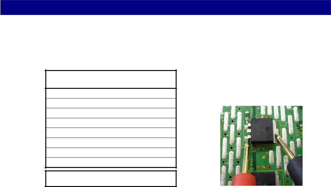
Block1. Short Circuit Check of the Switching Component and Diode
< 2012 model >
Check the short circuit “all” of the below switching components. ( just check short or not )
In many cases, there are several defective components at the same time.
Check parts ( Defective parts ) :FET(D-S) , Transistor (C-E) , Diode (K-A)
Q16401 - 404 / D16401 - 404
Q16421 - 424 / D16421 - 424
Q16621 - 625 / D16641 - 644
Q16661 / D16673 - 674
Q16660 / D16652 Full HD Only
Q16600 - 601 / D16618, R16601 ( open check)
Q16441 - 443 / D16481 - 483
Q16451 - 453 / D16461 - 463
D16430, D16432, D16434, D16435
D16722, D16723, D16725
The Scan board is producing the scan pulse output (VFO and VFG) by switching of several kinds of voltage. ( refer to the next page )
In main case of the defect, these switching parts are short-circuited.
14

BLOCK1 Drive Circuit ( Switching Control Signal ) |
< 2012 model > |
|
|
If drive IC is defect (=always output switch-on signal), the switching component
must be damaged. Check also the drive circuit when the switching component is defect.
< example: IC16501,16521 >
IC16501
Buffer (Drive IC)
VDD
IN OUT
(GND)
VOL+15V
VOL
IC16521
Buffer (Drive IC)
VDD
IN OUT
VS
15V GND
If these switching components are defect, check also Drive components.
Vsus
Q 
R
C VOL
Vsus
VOL
GND
VOL
Q
R
C
15

|
How to check the Drive ICs and Power IC |
|
|
< 2012 model > |
||||
|
|
We can check the power IC and drive IC by DIODE CHECK. |
|
|
|
|||
|
|
The check terminal is as below. |
|
|
|
|
||
|
|
|
IC |
|
Diode check ( Check pin : Normal voltage ) |
|
||
|
BLOCK1 |
|
Except |
IC16501, 16502, 16521, 16522 |
1pin (+) and 4 pin(-) : 0.45V +/- 0.2V |
|
||
|
|
|
T*-P42GT50/ST50/UT50 |
(IC15603,16504,16523,16524) |
1pin (+) and 7 pin(-) : |
0.45V +/- 0.2V |
|
|
|
|
|
(Except TNPA5523/5620) |
(Drive signal for |
1pin (+) and 8 pin(-) : |
0.5V +/- 0.2V |
|
|
|
|
|
|
switching components) |
|
|
|
|
|
|
|
Only |
IC16501, 16502, 16521, 16522 |
3pin (+) and 1 pin(-) : |
0.5V +/- 0.2V |
|
|
|
|
|
T*-P42GT50/ST50/UT50 |
(Drive signal for |
3pin (+) and 2 pin(-) : |
0.55V +/- 0.2V |
|
|
|
|
|
(TNPA5523/5620) |
switching components) |
3pin (+) and 7 pin(-) : |
0.55V +/- 0.2V |
|
|
|
BLOCK3 |
|
IC16784, IC16786 |
|
8pin (+) and 1 pin(-) : |
0.45V +/- 0.2V |
|
|
|
|
|
(power IC) |
|
8pin (+) and 3 pin(-) : |
0.6V +/- 0.2V |
|
|
|
(Explanation |
|
|
8pin (+) and 4 pin(-) : |
0.6V +/- 0.2V |
|
||
|
is as later |
|
|
8pin (+) and 5 pin(-) : |
0.45V +/- 0.2V |
|
||
|
page) |
|
IC16795 |
|
2pin (+) and 1 pin(-) : |
0.5V +/- 0.2V |
|
|
|
|
|
(power IC) |
1 2 3 |
2pin (+) and 3 pin(-) : |
0.45V +/- 0.2V |
|
|
|
|
|
|
Vout com Vin |
|
|
|
|
|
|
|
|
|
|
|
|
|
|
|
|
IC16725 |
|
12pin (+) and 1 pin(-) : |
0.5V +/- 0.2V |
|
|
|
|
|
(power IC) |
|
12pin (+) and 24 pin(-) : |
0.4V +/- 0.2V |
|
|
|
Don’t mistake the polarity. |
|
|
|
example |
|||
Diode check |
0.6V |
+ |
- |
i
16

Block2. Short circuit check of Scan Drive IC (Only SN Board) |
< 2012 model > |
|
|
Check the short circuit between VFG and VFO. If shorted, some of the Scan Drive IC is |
|||||||||
defective. You can find the defective IC by checking the short circuit between VFG and |
|||||||||
all output pin of Scan Drive IC (same as all pin of Connector SN11-18/21-28). |
SN11/21 |
||||||||
|
|
|
Vsus |
Vsus |
Vscn |
|
TPSC1/ |
IC14901 |
|
|
|
|
|
Scan |
|
||||
|
|
|
|
|
|
|
TPSN1 |
Drive |
|
|
|
Q16401 |
|
|
|
|
|
IC |
SN12/22 |
|
|
|
|
|
|
|
|
||
|
|
- 403 |
|
|
|
|
|
|
|
|
|
|
|
|
|
|
Scan |
|
|
|
|
|
|
|
|
|
|
|
|
|
|
|
|
Q16600 |
|
|
VF0 |
Drive |
|
|
|
|
|
|
|
IC |
|
||
|
|
|
|
|
|
|
|
|
|
( Energy recovery circuit ) |
|
-601 |
+ |
|
|
IC14902 |
|
||
|
|
|
|
|
|||||
|
|
Vscn |
|
. |
|||||
|
L16411 |
|
|
|
- |
. |
|||
C16631- |
|
|
|
|
|
. |
|||
-12 |
|
|
|
|
|
|
. |
||
632 |
|
|
VOL |
|
|
|
|
. |
. Output pin |
|
|
Q16441 |
|
|
- |
|
VFG |
IC14953 |
SN17/27 |
|
|
|
|
Vad |
|
|
|
||
|
|
|
Q16621 |
|
|
|
|
||
|
|
-443 |
|
+ |
|
|
Scan |
|
|
|
|
|
|
|
|
|
|
|
|
|
Q16451 |
|
|
-623 |
|
|
|
Drive |
|
|
|
|
|
|
|
IC |
SN18/28 |
||
|
|
|
|
|
|
|
|
||
|
-452 |
|
Q16421 |
Q16661 |
|
|
Scan |
|
|
|
GND |
|
|
-423 |
|
|
|
Drive |
|
|
|
|
|
|
|
IC |
|
||
|
|
|
GND |
|
GND |
|
|
IC14954 |
|
|
|
|
|
|
|
|
|
||
|
|
|
|
|
|
|
Scan Drive IC |
|
|
|
|
|
|
|
|
|
|
|
|
SN board of HD model (not full-HD model) |
|
|
|
|
Only SN board |
Output pin |
|||
SN2 |
|
|
|
|
Check short circuit |
|
(SC board is |
||
D16461 |
D16481 |
|
|
|
|
||||
|
|
|
(refer to next page) |
|
separated to |
|
|||
|
|
|
|
|
|
SU/SD board) |
|
||
|
|
|
|
|
|
|
|
|
|
To |
|
L16441 |
|
|
PSS |
|
|
||
Q16451 |
Q16441 |
|
||
board |
17 |
|||
|
|
BLOCK2. Short circuit check of Scan Drive IC (Only SN Board)
All
Output
pin
VF_G
18

How to replacement of PDP Scan Driver IC on SNSN boardboard 1/2
1. Remove silicon glue by plastic plate.
2. After removal, put the low temperature solder(Part No.:RFKZ0316) on to the solder of IC.
3. Remove IC
Remove by tweezers
4. Cleaning
Low temperature solder |
Blotting wire |
(Local procurement) |
|
(Part No.: RFKZ0316) |
|
Completion

How to replacement of PDP Scan Driver IC on SNSN boardboard 2/2
5. Installation of IC
Positioning
6. Cleaning
Washing
7. Spreading of silicon glue
Silicone glue (Part No.: T8CJ011)
Incase of Local procurement
*Product name:
DOW CORNING(R) SE9189L GRAY RTV http://www.dowcorning.com
Soldering |
Completion |
Wiping |
Completion |
spread |
Thicken time : 10 minute |
|
|
|
The installation complete |
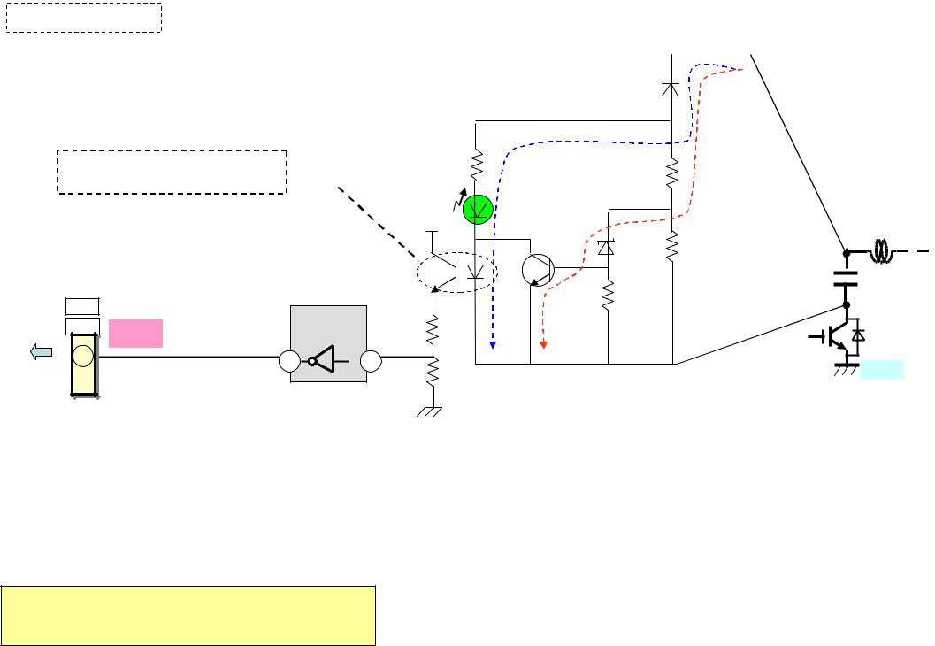
Block Diagram of Power Supply Circuit |
< 2012 model > |
|
|
All power supply circuit start automatically, when Vsus is input.
Vad, Vscn, F15V, and 5V_F are regulated from VFG.
So when you check the voltage, please confirm that basis is VFG.
SC2 SN2 |
||
1 |
Vsus(205V) |
|
6 |
||
P board |
+ |
|
C16411 |
||
|
||
|
-415 |
|
3 |
1 |
|
|
Full-HD model only |
|
|
SN20 |
|
|
SC20 |
P5V |
|
30 |
|
|
|
|
A board |
1 |
P15V |
2 |
|
D16711 Vad
|
(60V) |
|
T16471 |
Vad2 + |
(200V) |
|
T16472 |
|
|
+ |
C16813 |
|
|
|
|
VFG |
|
DC/DC |
D16712 |
DC/DC |
DC/DC |
|
DC/DC |
IC16784 |
|
IC16786 |
IC16784 |
|
IC16786 |
GND |
GND |
D16713 Vscn (TPSC1)
-714 |
(147V) |
|
|
|
|
|
|
|
|
|
|
||
+ |
|
|
|
|
|
|
C16842 |
D16728 |
(F20V) |
|
F15V |
Regulator |
F5V |
Regulator |
|
|||||
|
|
|
5 |
Regulator |
||
|
|
3 Regulator 1 |
// 22 |
|
||
|
+ |
|
IC16795 |
|
Detection |
|
|
|
|
Detection |
(5V) |
||
|
|
|
IC16795 |
(14.6V) |
IC16725 |
|
VFG |
C16793 |
(18V) VFG |
IC16725 |
|
||
|
VFG |
|
||||
|
|
|
||||
|
|
|
|
|
|
|
The value is one example of 50ST50 product. (Vad / Vscn are different by each model)
Please check the accurate value by Service Manual21.
Block3. Short Circuit Check of Power Line and Check the Output Voltage
Check the short circuit of power line. If it is not short circuited, |
< 2012 model > |
|
then check the output voltage with the unit just before shutdown.
The block diagram of power supply circuit is described to the next page.
Symptom |
Output voltage / Check parts |
Basis of output voltage (*3) |
Output voltage value |
(just for reference) |
|
|
(*1: Depend on the model) |
Except 6,7 blinks |
Vsus : input from P board |
From GND |
213V/210V/189V from GND |
|
(C16411 – 16415, 16507) , |
|
|
|
|
|
|
Except 6,7 blinks |
P15V : input from P board |
From GND |
15.6V from GND |
|
(R16503, 536, 537,605,618, 902, |
|
|
|
D16536, C16502, 505, 531, 891 ) |
|
|
|
|
|
|
7 blinks |
Vad |
from VFG |
205V/200V/195V from VFG |
|
( IC16784(*2) or D16833, T16471, |
|
(*3) |
|
IC16785, PC16897 ) |
|
|
|
|
|
|
7 blinks |
Vscn , 16V_F |
from VFG |
147V from VFG (*3) |
|
( IC16786(*2) or D16720, T16472, |
|
18V from VFG (*3) |
|
IC16787, PC16723 ) |
|
|
|
|
|
|
7 blinks |
15V_F |
from VFG |
14.6V from VFG (*3) |
|
( IC16795(*2) ) |
|
|
|
|
|
|
7 blinks |
5V_F |
from VFG |
5V from VFG (*3) |
|
( IC16725(*2) ) |
|
|
(*1) This value is different by each model. So please check the accurate value by the Service Manual.
(*2) The check of these components is not only short circuit check also diode check.
Refer to the later page.
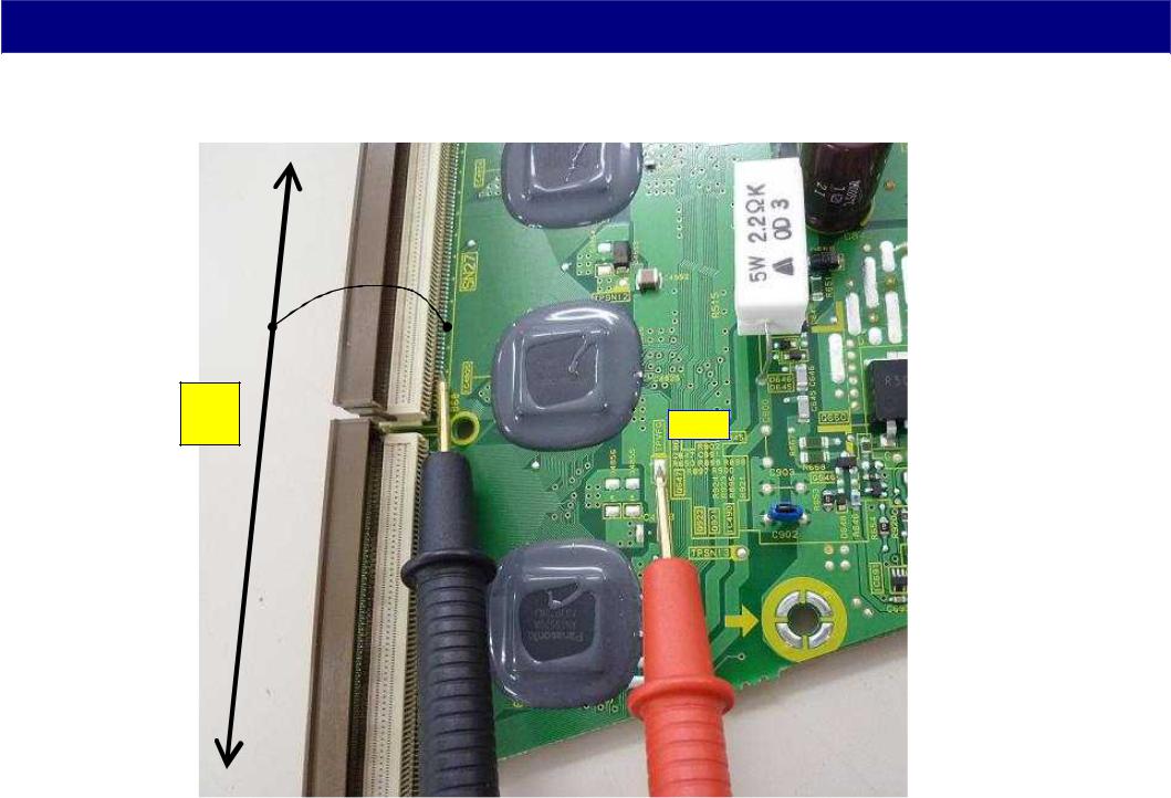
(*3) Be careful
The basis is not GND.
If you check by oscilloscope,
don’t plug in the ground pin (3rd pin) of the oscilloscope.
Isolate it from the earth of AC inlet.
Ground pin (3rd pin)
( This picture is a Japanese type ) |
22 |
Other Block. Check the SOS Circuit-1 ( 2012 Full HD |
|
< 2012 model > |
||
|
|
|
|
|
|
Monitor MID |
|
|
|
|
|
|
|
|
|
|
|
(Low V= stop) D16581 |
|
|
|
|
|
|
|
(33V) |
|
|
If this voltage is out of range, |
Normal = on |
56k |
Normal |
47k+47k |
|
|
|
|
|
||||
PC16581 is change to off. |
|
|
|
|
||
LED |
|
D16582 |
High V |
|
|
|
|
|
|
L16411 |
|||
|
P15V |
|
|
|
||
|
|
|
|
|
||
|
|
|
|
ERM |
-13 |
|
|
|
|
(33V) |
37.4k |
||
|
|
|
|
|
ERF |
|
PC16581
|
|
|
(Photo coupler) |
|
10k |
(=about half of Vsus) |
C16631 |
|
SN20 |
|
|
|
|
Q16581 |
ERR |
-632 |
|
|
|
Inverter |
|
|
|
|
||
SC20 |
SOS6 |
|
|
|
|
|
Q16451 |
|
|
(IC16563) |
(5V) |
47k |
|
|
|||
28 |
|
|
|
|
|
|
-452 |
|
(Normal = Low) |
8 |
|
9 |
|
|
|
GND |
|
A baord |
|
22k |
|
|
||||
|
|
|
|
|
||||
If this signal is high(5V), 6blinks occurred.
The value is one example of 50ST50 product. |
|
(Vscn / Vad and Zener diode are different by each model) |
23 |
Please check the accurate value by Service Manual. |

Other Block. Check the SOS Circuit-2 |
< 2012 model > |
|
|
Monitor 15V_F / 5V_F
P5V
SN20 |
SC20 |
25 |
|
Buffer |
|
(IC |
|
16563) |
4 |
3 |
SOS7
A baord Hi = SOS
Low = enable
19
Buffer (IC16561)
|
Buffer |
|
(IC |
|
16563) |
2 |
1 |
|
main_stop0 |
|
(Normal = Low) |
PC16480
(Photo coupler)
Normal = on
Switching signal for Scan output
Vdd (DC/DC of Vad) |
Vad |
(6V) |
|
|
|
|
|
Vdd (DC/DC of Vscn)(6V) |
|
|
PC16896
VFG
|
|
|
|
|
|
|
If (F18V) rises than 25.2V from VFG |
|
|
|
|
|
|
|
|
|
|
|
|
||||||||||
|
|
|
|
|
|
|
or F5V drops below 3.5V from VFG |
|
|
|
|
|
|
|
|
|
|
|
|
||||||||||
|
|
|
|
|
|
|
or CHA line cuts, |
|
|
|
|
|
|
|
|
|
|
|
|
|
|
|
|
|
|||||
|
|
|
|
|
|
|
FET of 18 pin switch off. |
|
|
|
|
|
|
|
|
|
|
|
SU |
||||||||||
|
|
F5V |
|
|
|
|
|
|
|
|
|
|
|
SU |
|||||||||||||||
|
|
|
|
|
|
|
|
|
|
|
|
|
|
|
|
|
|
|
|
|
|
|
|
||||||
|
|
|
|
|
|
|
Then photo coupler changed to off, and |
|
|
|
|
|
Board |
||||||||||||||||
|
|
|
|
|
|
|
|
|
|
|
|
Board |
|||||||||||||||||
|
|
|
|
|
|
|
main_stop0 signal changed to high. |
|
|
|
|
|
|
|
|
|
|
||||||||||||
|
560 |
|
|
|
|
|
|
|
|
|
|
|
|
|
|
|
|
|
|
|
|
|
|
|
|
||||
|
|
|
|
|
|
|
|
IC16725 |
F15V |
|
|
|
|
|
|
|
|||||||||||||
|
|
|
|
|
|
|
|
|
|
|
|
|
|
||||||||||||||||
|
|
|
|
|
|
|
|
|
|
|
|
|
|
|
|
|
|
|
|
||||||||||
|
|
|
|
|
|
|
|
|
|
|
|
|
|
|
|
|
|
|
|
||||||||||
|
|
|
|
|
|
|
|
|
|
|
|
|
(F18V) |
VFG |
|
|
|||||||||||||
|
|
|
|
|
|
|
|
|
|
|
|
|
|
|
|
|
|
|
|
||||||||||
|
|
|
|
|
1k |
|
(F18V) |
|
|
|
|
|
|
|
|||||||||||||||
|
|
|
|
|
|
|
|
5.6k |
|
CHA |
|
|
|
||||||||||||||||
|
|
|
|
|
|
|
|
|
|
|
|
||||||||||||||||||
|
|
|
|
|
|
|
|
|
|
|
|||||||||||||||||||
|
|
|
|
|
|
|
|
|
|
|
|
|
|
|
D16791 |
|
|
|
|
|
|
||||||||
|
|
|
|
|
|
|
|
|
|
|
|
|
|
|
|
|
|
|
|
|
|
|
|||||||
|
|
|
|
|
|
|
|
|
|
|
|
|
|
|
|
|
20 |
|
|
|
|
||||||||
|
|
|
|
|
|
|
|
|
|
|
|
|
|
|
|
|
|
|
|
|
|
|
|
|
|||||
18 K |
REF |
20k |
|
(24V) |
|
|
|
IC16471 |
|
Q16471 |
1k |
D16475 |
|
|
|
7 |
|
7 |
(5.1V) |
|
|
||
Shunt |
|
|
|
|
|
|
|
REG |
|
2.2k |
|
|
|
|
|
A |
|
|
|
10k |
SC50 |
SD |
|
|
|
|
|
2 |
|||
VFG |
|
VFG |
|
|
|
SD |
|
VFG |
|
VFG |
|
|
|
board |
|
|
|
|
|
|
|
1 |
board |
|
Vscn Vad |
|
VFG |
|
5V_F |
||
|
|
|
|
||||
|
|
|
|
|
|
|
VFG |
D16473
59k |
(Normal = High) |
SCNR_PRO |
|
||
|
|
|
82k+61.9k |
|
|
(Vz=33V)
Q16815 |
10k |
37.4k |
VFG VFG
If Vscn or Vad rises,
Transistor Q16815 is ON.
The value is one example of 50ST50 product.
Please check the accurate value by Service Manual. 24

Other Block. Check the Feedback Circuit |
< 2012 model > |
|
|
Monitor VOL ( feed back to control IC)
SN20 |
|
|
|
SC20 |
|
|
Inverter |
|
|
|
|
|
UHZ |
(IC16563) |
|
22 |
|
|
|
|
6 |
5 |
|
|
|
||
This signal is Feedback signal to discharge control IC on A board.
(If no feed back, 8 time blinks)
The value is one example of 50ST50 product.
|
|
|
|
P15V |
|
|
|
|
|
22.6k |
|
|
|
|
|
VTH2 |
|
|
Comparator |
|
|
1.47k |
|
|
|
|
VTH1 |
|
|
|
(IC16921) |
|
|
|
|
|
+ |
|
8 |
976 |
|
|
- |
|
7 |
VTH3 |
|
|
|
|
|
|
|
12 |
|
|
|
5.23k |
Vad |
|
|
|
|
||
LO |
|
|
|
|
69.8k+82.5k+82.5k |
L |
|
|
|
RAMP1 |
|
|
|
|
=234.8k |
||
O |
+ |
REF 1.2V |
|
|
3.09k |
G |
|
|
|||
- |
|
9 |
RAMP2 |
|
|
I |
|
|
|
7.87k |
|
|
|
|
|
||
C |
|
|
|
|
|
|
|
|
VOL |
|
|
|
|
|
|
|
|
|
|
|
|
120k+120k+120k |
|
|
+ |
|
10 |
=360k |
|
|
REF 2.5V |
RAMP3 |
|
||
|
- |
|
|
||
|
|
5.11k |
|
||
|
|
|
|
|
25 |

Supplement ( flow of control signal for scan pulse switching < 2012 model >
Scan pulse output waveform is produced by the many switching.
|
Vsus |
Vsus |
|
Q16401 |
|
IGBT |
- 403 |
|
Driver1 |
|
Q16600 |
(IC16503) |
|
-601 |
CMH |
|
|
FET
Driver1
(IC16600)
CPH1,CSH
|
|
|
|
|
|
|
|
|
|
|
|
|
Vscn |
|
Vscn shifted |
||||||||||
|
|
|
|
|
|
|
|
|
|
|
|
|
|
|
|
|
|
|
|
|
|
|
|
|
|
|
|
|
|
|
|
|
|
|
|
|
|
|
|
|
|
|
|
|
|
|
|
|
|
|
|
|
|
|
|
|
|
|
|
|
|
|
|
|
|
|
|
|
|
|
|
|
|
|
|
|
|
|
|
|
|
|
|
|
|
|
|
|
|
|
|
|
VF0 |
|
+ |
|
To |
|
Vscn |
SU/SD |
||
|
|||
- |
board |
||
|
|||
|
|
L16411-12 |
VOL |
|
|
|
VFG |
|
|
|
|
|
|
||
|
|
|
|
|
|
|
C16631 |
Q16441 |
|
|
|
|
|
-632 |
-443 |
|
Q16621 |
|
- |
|
|
|
|
|
|
||
|
|
|
-623 |
|
Vad |
|
Q16451 |
IGBT |
|
|
|
+ |
|
-452 |
Q16421 |
|
|
|
|
|
|
Driver4 |
|
|
|
|
|
GND |
(IC16504) |
-423 |
|
|
Q16661 |
|
CSH,nCPH1 |
|
IGBT |
|
|
||
|
|
|
|
|
||
|
|
GND |
Driver5 |
|
|
Vad2 |
IGBT |
|
(Q16762) |
|
GND |
||
|
|
CIS,CEL |
|
|
|
|
Driver3 |
IGBT |
|
IGBT |
|
|
|
|
|
CELR |
|
|||
(IC16524) |
Driver2 |
|
|
Driver6 |
Q16646,647,660 |
|
CSL |
|
|
|
|||
(IC16523) |
|
|
(IC16921) |
|
||
|
|
|
|
|||
CML |
nCEL, |
26 |

<![endif]>Supplement ( flow of control signal for scan pulse switching
< 2012 model >
PC16461
PC16462
PC16461
IC16523
IC16524
Q16820
PC16685
Q16646,647,660
SD board
SD board
|
SD board |
|
|
IC16921 |
|
|
PC16685 |
|
|
Q16921(IC16921) |
|
IC16561 |
||
27 |
||
|

< 2012 model >
2-2-1.Check List of HD model-SN Board
T*-P42X5/X50/C5/C50*, TC-P46X5* :TNPA5592**
T*-P50X5/X50/C5/C50* :TNPA5593**
Check all components of this list, then try to power on.
28
|
Check List (1/2) |
|
|
|
|
< 2012 model > |
|||||
|
< HD model-SN board > |
|
|
|
|
|
|
|
|
||
|
|
T*-P42X5/X50/C5/C50*, TC-P46X5* :TNPA5592** |
|
|
|
|
|
|
|||
|
|
T*-P50X5/X50/C5/C50* |
:TNPA5593** |
|
|
|
|
|
|
||
|
|
|
|
|
|
|
|
||||
|
|
|
|
|
|
|
( ### )notation: only 50inch model=TNPA5593** |
|
|||
|
|
|
|
|
|
|
|
|
|
|
|
|
|
|
Reference No. |
|
Check |
(Drive Circuit) |
|
Check |
|
|
|
|
BLOCK1 |
|
Q16401, Q16402, D16401, D16402, (D16403) |
|
IC16501, R16401, R16402 |
|
|
|
|
||
|
|
|
#:Because of parallel circuit, check one of 5. |
|
|
|
|
|
|
|
|
|
|
|
Q16421, Q16422, D16421 |
|
|
IC16521, R16421, R16422 |
|
|
|
|
|
|
|
|
#:Because of parallel circuit, check one of 3. |
|
|
|
|
|
|
|
|
|
|
|
Q16621, Q16622, D16641, D16642, (D16643) |
|
Q16762, R16761, R16621, R16622, |
|
|
|
|||
|
|
|
#:Because of parallel circuit, check one of 5. |
|
R16681, R16682 |
|
|
|
|
||
|
|
|
Q16661, D16673, D16674 |
|
|
D16668, R16661 |
|
|
|
|
|
|
|
|
#:Because of parallel circuit, check one of 3. |
|
|
|
|
|
|
|
|
|
|
|
Q16601, D16618, R16601 |
|
|
IC16600, R16612 |
|
|
|
|
|
|
|
|
Q16441, D16481 |
|
|
IC16502, C16531, R16441 |
|
|
|
|
|
|
|
|
#:Because of parallel circuit, check one of 2. |
|
|
|
|
|
|
|
|
|
|
|
Q16451, D16461 |
|
|
IC16522, C16551, R16451 |
|
|
|
|
|
|
|
|
#:Because of parallel circuit, check one of 2. |
|
|
|
|
|
|
|
|
|
|
|
D16432, D16435, D16722, D16723, D16725 |
|
--- |
|
|
|
|
|
|
If defective, check also drive circuit
Q##, D## C## : Short check, R## : Open check, IC## : Diode check (refer to later page)
29

Check List (2/2) < 2012 model >
< HD model-SN board >
T*-P42X5/X50/C5/C50*, TC-P46X5* :TNPA5592** T*-P50X5/X50/C5/C50* :TNPA5593**
|
Reference No. |
Check |
BLOCK2 |
Short check between VFG and VFO. |
|
|
If shorted, then short check output of each scan drive IC, |
|
|
IC14901, 14902, 14903, 14904, 14951, 14952, 14953, 14954 |
|
BLOCK3 |
IC16784, D16833, C16833 |
|
|
IC16786, D16720, C16834 |
|
|
IC16795, C16793, C16796 |
|
|
IC16725, C16723, C16724, C16725 |
|
|
C16411, C16412 |
|
|
#:Because of parallel circuit, check one of 2. |
|
Q##, D##, C##, IC14### : Short check, R## : Open check, IC16### : Diode check (refer to later page)
30
 Loading...