


!
Plasma Sub Field Drive Recap:
The 3 phases for firing pixels are given below and is called a SUBFIELD:
INTIALISE ----Æ ADDRESS (SCAN) ----ÆSUSTAIN
These steps create light from pixels.

 3-1. Sub Field
Purpose:
Control Each Pixel’s Brightness Individually
(Set up) |
|
(Scan & Write) |
|
(Emission) |
|
|
|
|
|
Initialize |
|
Address |
|
Sustain |
Address |
Sustain |
Period |
Period |
One Sub Field |
|
1 Initialise phase resets all pixels
2 Scan phase writes WALL VOLTAGE to all pixels on a line by line basis
3 Sustain phase drives the entire screen to produce brightness from the pixels that have wall voltages loaded.
1
!
Brightness Control
Analogue Video Signal |
8 Bit Digital Video Signal |
1st Line
120th Line
240th Line
Sampling point
CLICK
|
|
|
|
|
|
|
|
|
|
|
|
|
|
|
1 |
|
1 |
|
1 |
|
1 |
|
1 |
|
1 |
|
1 |
|
1 |
: |
|
: |
|
: |
|
: |
|
: |
|
: |
|
: |
|
: |
0 |
|
1 |
|
1 |
|
1 |
|
1 |
|
1 |
|
1 |
|
0 |
: |
|
: |
|
: |
|
: |
|
: |
|
: |
|
: |
|
: |
1 |
|
1 |
|
1 |
|
0 |
|
0 |
|
0 |
|
0 |
|
0 |
|
|
|
|
|
|
|
|
|
|
|
|
|
|
|
1st Sub Field |
4th S.F. 7th S.F. |
2nd S.F. |
5th S.F. 8th S.F. |
3rd S.F. 6th S.F.
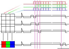
Sub Field Drive System
The above slide shows how each sample (from a video line) is driven on the screen using SUB FIELDS (SF)
•Each colour line (R, G and B) of video is sampled 852 times per line (with typically 8 bits per sample). This info is stored in D board memory for the whole frame.
Addressing consists of INITIALISATION + SCANNING:-
•INITIALISE STAGE (resets all pixels):
•Firstly, all scan lines are initialised using the TPSC drive (see page 6) i.e. all outputs of the SU/SD boards are switched to Vf output (initialise pulse is output at 400V to all lines). The sustain lines are also driven to their respective levels in this stage (see page 5 for TPSS/SC waveform timing during the 3 phases).
SCANNING PHASE (Writes each panel line with wall voltages using data drive signals)
•After INITIALISATION the SCAN period occurs: Firstly, all scan lines are connected to Vf0 waveform (+30v in scan period) via the SU/SD boards.
•The drive signals to the SU/SD boards (see page 12) successively takes each line LOW to -90v i.e. Vf level for typically 2 micro second duration. All other non scanned lines are held OFF at +30V Vfo level. This can happen
2
!
because the Vf and Vfo waveforms are at different levels during the SCAN period-see page 5 for more information
Vertical Scan
R Data
G Data
B Data
Y1 

Y2 

Y3 

//
//
//
//
//
//
Initialization Vertical Scan
Y480 |
// |
|
CLICK3 times  1 Sub Field
When a line is taken -90v; data is fired up the (852x3 = 2556 columns) data drivers to allow a single horizontal line of WALL VOLTAGE to be written using the 67V data pulses sent up from the bottom data drivers. This is the RGB binary sample data from D board memory for the line being scanned. See above for address period scanning principle.
This is repeated for all lines using the first bit of the 8 bit sample (1st sub field) until the entire screen’s lines have had WALL VOLTAGE written to them.
Pixels that will be lit (in the sustain phase) have had data pulses of 67v supplied. Pixels receiving no wall voltage i.e. logic ‘0’ will not light. Date driver control signals during the scan phase are as per page 16
The whole scan period is typically 1 milli second and in this time all 480 lines (SD panel) are taken low in turn.
SUSTAIN PHASE:(lights up all the scanned pixels containing wall voltage):
After scanning the whole screen, all pixels are now ready to be fired on. Only the pixels with wall voltage i.e. data ‘1’ loaded during SCAN phase will fire during sustain.
Sustain electrodes are all driven at the same time with TPSS waveform. The SU/SD boards now output the Vf drive waveform to all lines during this stage.
•Sustain phase creates a fixed intensity discharge (brightness) for a certain amount of time (which is increased for each subsequent sub field).
3
!
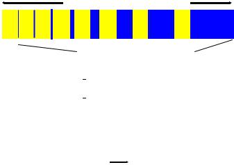
•The picture is then re-SCANNED using the next significant data bit from the frame video sample being displayed. However, the next sub field’s sustain period duration (when brightness is produced) is now made larger to create a brighter subfield which reflects the bit’s brightness value in the original 8 bit sample.
•This period of sustain is made larger for successive subfields as below. The YELLOW SECTIONS are the total address period (initialisation + scan) which is fixed per subfield. The BLUE shows the increasing (binary weighted) sustain period per sub field.
Brightness Control
8 Sub Fields
1 2 4 8 16 32 64 128
Very Bright |
|
|
|
|
|
|
|
|
|
|
|
|
|
|
|
111 1 |
1 |
1 |
1 |
1 |
|
|
|
||||||||
|
|
||||||||||||||
Bright |
|
|
|
|
|
|
|
|
|
|
|
|
|
|
|
|
|
|
|
|
|
|
|
|
|
|
|
|
|
|
|
100 |
1 |
0 |
0 |
0 |
1 |
|
|
|
|||||||
Dark |
|
|
|
|
|
|
|
|
|
|
|
|
|
|
|
|
|
|
|
|
|
|
|
|
|
|
|
|
|
|
|
111 |
0 |
1 |
0 |
0 |
0 |
|
|
|
|||||||
|
|
||||||||||||||
Very Dark |
|
|
|
|
|
|
|
|
|
|
|
|
|
|
|
|
|
|
|
|
|
|
|
|
|
|
|
|
|
|
|
010 |
0 |
0 |
0 |
0 |
0 |
Pixels |
|||||||||
CLICK |
|
t |
|
|
|
|
|
|
|||||||
|
|
|
|
|
|
|
|
|
|
|
|||||
•8 sub fields (pictures) are produced for each video frame. This conveys the brightness of all the bits in the samples for one frame in 8 separate levels.
•The above picture shows that samples with all ‘1’s appear
very bright after 8 subfields since each of the 8 pictures (subfields) are producing light. The dark samples (low video level) produce no or low light output over the 8 subfields because the data bits are only ‘1’ for a few subfields i.e. total light (blue sections) output is lower from the darker pixels.
•The process is then repeated for the other frames. In practice 10 to 14 variable linear (as opposed to binary weighted) sub field drive is used to minimise motion problems and power consumed
4

!
How to Check: SC, SS, SU/SD drive waveforms and data drives
Scope check the TPSC and TPSS drive waveforms (on SC, SS boards) and see if the voltage levels of the 3 stages in the drive waveforms are correctsee service manual for voltage levels and 3 stages of waveforms: INITIALISE, SCAN, SUSTAIN.
NOTE: The SC BOARD produces 2 drive voltages:
Vfo |
which is TPSC |
Vf |
which is measured on the SU/SD gnd plane |
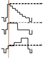
A typical TPSC waveform and exploded view of the 3 drive sections are shown below:
Initialize period |
scan period |
sustain section period |
5
 Loading...