


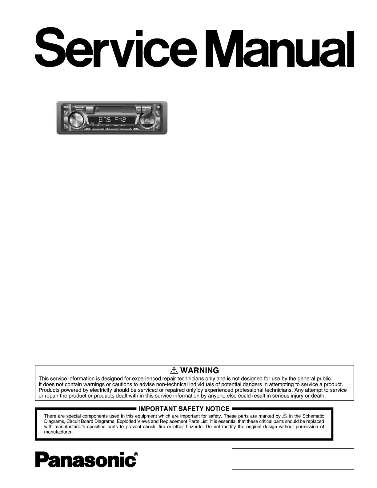
CQRG-133-W-1
General
Power Supply DC 12V (11V - 16V),
Test Voltage 14.4V
Negative Ground
Tone Controls Bass ; ±12dB at 100Hz
Treble ; ±12dB at 10kHz
Current Consumption Less than 2.5A (Tape play mode,
0.5W×4ch)
Maximum Power Output 40W×4ch (at 400Hz, Vol. Max.)
Suitable Speaker Impedance 4-8Ω
Pre-Amp Output Voltage 2V (CD play mode; 1kHz, 0dB)
Output Impedance 200Ω
FM Stereo Radio
Frequency Range 87.5 - 108.0MHz
Usable Sensitivity 12.0dBf (1.1µV, 75Ω)
Frequency Response 30Hz to 15,000Hz (±3dB)
Alternate Channel Sensitivity 75dB
Stereo Separation 35dB(1kHz)
Signal to Noise Ratio 70dB(Mono)
© 2005 Matsushita Electric Industrial Co., Ltd. All
rights reserved. Unauthorized copying and
distribution is a violation of law.
CQ-RG133W1
Removable Face High-Power Cassette /
Receiver with Changer Control
AM Radio
Frequency Range 531 - 1,602kHz
Usable Sensitivity 28dB/µV (25µV, S/N 20dB)
Tape Player
Reproduction System 4-track,2-program stereo
Tape Speed 1-7/8” /sec (4.76cm/sec)
FF/REW Time Less than 200 sec (C-60)
Wavelength 780nm
Frequency Response 35Hz to 14,000Hz (±3dB)
Signal to Noise Ratio 52dB
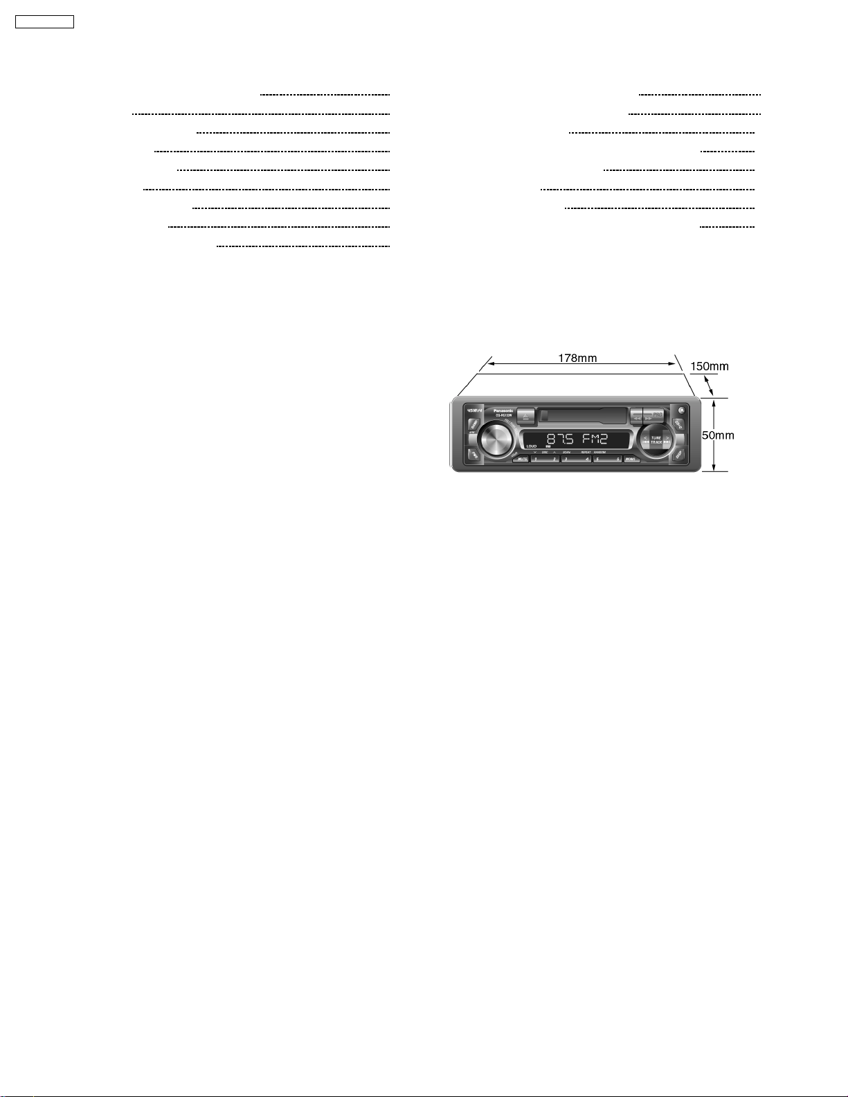
Dimensions** 178×50×150mm
Weight** 1.6kg
* Specifications and the design are subject to possible modification
without notice due to improvements.
** Dimensions and Weight shown are approximate.
AUTOMOTIVE AFTERMARKET
Specification*
Order No. ACED050522C3
1 ABOUT LEAD FREE SOLDER (PbF) 2
2 FEATURES
2
3 REPLACING THE FUSE
2
4 MAINTENANCE
2
5 RADIO ALIGNMENT
2
6 DIMENSIONS
2
7 WIRING CONNECTION
3
8 BLOCK DIAGRAM
4
9 TERMINALS DESCRIPTION
5
1 ABOUT LEAD FREE
SOLDER (PbF)
Distinction of PbF PCB:
PCBs (manufactured) using lead free solder will have a PbF
stamp on the PCB.
Caution :
·
Pb free solder has a higher melting point than standard
solder; Typically the melting point is 50 - 70°F (30 -
40°C) higher. Please use a soldering iron with
temperature control and adjust it to 700 ± 20°F (370 ±
10°C). In case of using high temperature soldering iron,
please be careful not to heat too long.
·
Pb free solder will tend to splash when heated too high
(about 1100°F/600°C)
·
This lead free solder will be used for the products after
serial No. 1,000,001.
2 FEATURES
·
PLL (Phase Locked Loop) Synthesized Tuning
·
1DIN Size Body with Cassette Player,AM/FM Tuner, Power
AMP (30Wx4)
·
18-FM , 6-AM stations preset
·
Auto preset and scan function
·
CD Changer Control function
3 REPLACING THE FUSE
Be sure to use a fuse of the specified rating (10A) when
replacing a blown fuse. Fuses with higher capacity ratings,use
of any substitute, or connection without a fuse may result in a
fire hazard or damage to the unit.
4 MAINTENANCE
Your product is designed and manufactured to ensure a
minimum of maintenance. Use a soft cloth for routine exterior
cleaning. Never use benzine, or other solvent.
5 RADIO ALIGNMENT
Do not align the AM/FM package blocks. When the package
block is necessary, it will be supplied already aligned at the
10 PACKAGE AND IC BLOCK DIAGRAM 6
11 REPLACEMENT PARTS LIST (Unit)
8
12 EXPLODED VIEW (Unit)
12
13 REPLACEMENT PARTS LIST (Tape Player Parts)
13
14 EXPLODED VIEW (Tape Deck)
15
15 WIRING DIAGRAM
16
16 SCHEMATIC DIAGRAM
19
17 SCHEMATIC DIAGRAM for printing with A4 size
21
factory.
6 DIMENSIONS
CONTENTS
Page Page
2
CQ-RG133W1

7 WIRING CONNECTION
3
CQ-RG133W1
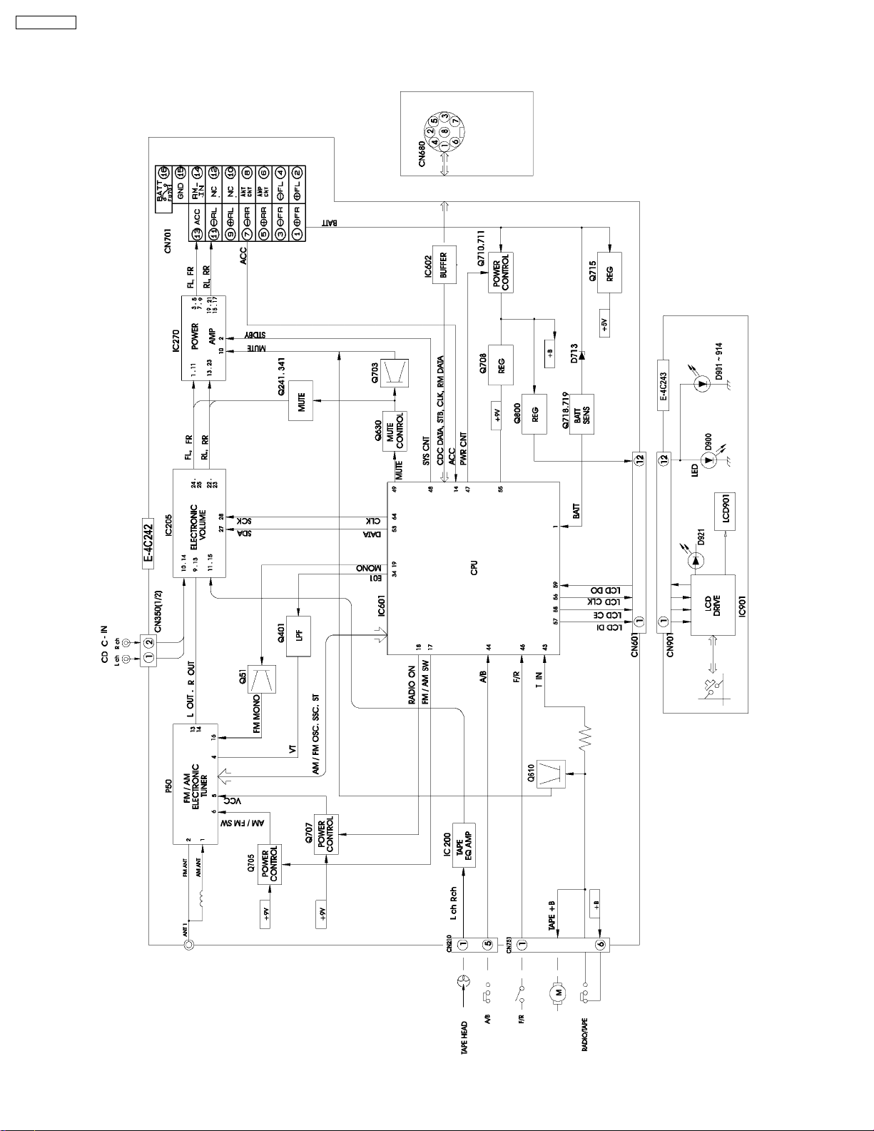
8 BLOCK DIAGRAM
4
CQ-RG133W1
IC601 : YEMLC72358N
Pin
No.
Port Descriptions I/O
(V)
FM
(V)
AM
(V)
TAPE
(V)
66 MODE B MODE B I 0 0 0
1 XIN Crystal Oscilator I 2 2 2
2 TEST2 TEST2 I 0 0 0
3 SI0/PG3 CD Changer Data I 0 0 0
4 SO0/PG2 - O - - -
5 SCK0/PG1 CD Changer Clock I 0 0 0
6 PGO Remoto Data Output O 0 0 0
7 SI1/PF3 LCD Data Output I 4.2 4.4 4.2
8 SO1/PF2 LCD Data input O 0 5 0
9 SCK1/PF1 LCD Clock O 5 5 5
10 PF0 LCD Chip Enble O 0 0 0
11 SI2/PE3 - O - - -
12 SO2/PE2 ALPS Rotary Encoder
Input
I 4.8 4.7 5
13 SCK2/PE1 In / Out Detection I 1 1 1
14 PE0 - O - - -
15 PD3 - O - - -
16 PD2 - O - - -
17 PD1 - O - - -
18 PD0 - O - - -
19 PC3 - O - - -
20 PC2 - O - - -
21 PC1 - O - - -
22 PC0 - O - - -
23 PB3 - O - - -
24 PB2 - O - - -
25 PB1 - O - - -
26 PB0 - O - - -
27 PA3 (Connect to Ground) I - - -
28 PA2 (Connect to Ground) I - - -
29 PA1 (Connect to Ground) I - - -
30 PA0 (Connect to Ground) I - - -
31 VDD Power supply +5V - 5 5 5
32 PQ0 - O - - -
33 PP3 System Power Control O 5 5 5
34 PP2 AMP ST-BY Control O 5 5 5
35 PP1 Mute Control O 5 5 0
36 PP0 Alarm LED Output O 0 0 0
37 PO3 Search Stop Control O 0 0 0
38 PO2 - O - - -
39 PO1 I2C Data O 5 5 5
40 PO0 I2C Clock O 5 5 5
41 PN3 - O - - -
42 PN2 - O - - -
43 PN1 - O - - -
44 PN0/BEEP - O - - -
45 PM3 - O - - -
46 PM2 - O - - -
47 PM1 - O - - -
48 PM0 - O - - -
49 PL3 - O - - -
50 PL2 Forward/Reverse Select I 0 0 5
51 PL1 - I 0 0 4.4
52 PL0 Tape In / Out Detection I 0 0 4.5
53 PK3 Battery Detection I 5.7 5.6 5.7
54 PK2 - O - - -
55 PK1/INT1 ALPS Rotary Encoder
Input
I 4.8 0 4.8
56 PK0/INT0 CD Changer Strobe I 0 0 0
57 PJ3 Power LED Output
Control
O 0 0 0
58 PJ2 FM MONO SW O 0 0 0
59 PJ1 Tuner On / Off Control O 0 0 7.1
60 PJ0 FM/AM Select Switch O 0 0 0
61 PI1/ADI5 (Connect to Ground) I - - -
62 PI0/ADI4 Mode Select B I 5 5 5
63 PH3/ADI3 Mode Select A I 0 0 5
Pin
No.
Port Descriptions I/O
(V)
FM
(V)
AM
(V)
TAPE
(V)
64 PH2/ADI2 Stereo Signal Input I 4.8 0 0
65 PH1/ADI1 FM SD Input I 0.77 2.5 0
66 PH0/ADI0 AM SD Input I 0.56 2.2 0
67 HOLD ACC Detection I 5.2 5.2 5.2
68 SNS Hot / Cold Detection I 4.6 4.5 4.6
69 LCTR (Connect to Ground) I
70 HCTR FM/AM IF Input I 2.3 2.3 0
71 EO3 - O - - -
72 SUBPD - O - - -
73 VDD Power supply +5V - 5 5 5
74 AMIN (Connect to Ground) I - - -
75 FMIN FM OSC Input I 2.2 2.3 0
76 VSS Ground - 0 0 0
77 EO2 - O - - -
78 EO1 FM / AM VT Output O 1.3 1.3 1.4
79 TEST1 TEST1 I 0 0 0
80 XOUT Crystal Oscilator O 2.5 2.5 2.5
9.2. Display Block
IC901 : YEAMLC75853NW
Pin No. Port Descriptions I/O
(V)
(V)
1-8 SEG1-8 LCD segment O 2.5
9-35 SEG9-35 LCD segment O 2.5
36-39 NC No connection - -
40-43 COM1-4 LCD common O 2.5
44-49 KS1-6 Key data output O 0.9
50-54 KI1-5 Key data input I 0
55 TEST (Connecting to ground) - 0
56 VDD +5V power supply - 5.1
57 VDD1 Ground through capacitor - 3.3
58 VDD2 Ground through capacitor - 1.7
59 Vss Ground - 0
60 OSC CR oscillator - 3.9
61 DO Key data output O 4.4
62 CE Chip enable I 0
63 CLK LCD clock I 0
64 DI LCD data input I 0
9 TERMINALS DESCRIPTION
9.1. Main Block
5
CQ-RG133W1
P50 CT-T02B
IC602 YEAMTC4584FN
IC 200 YEAMLA3161
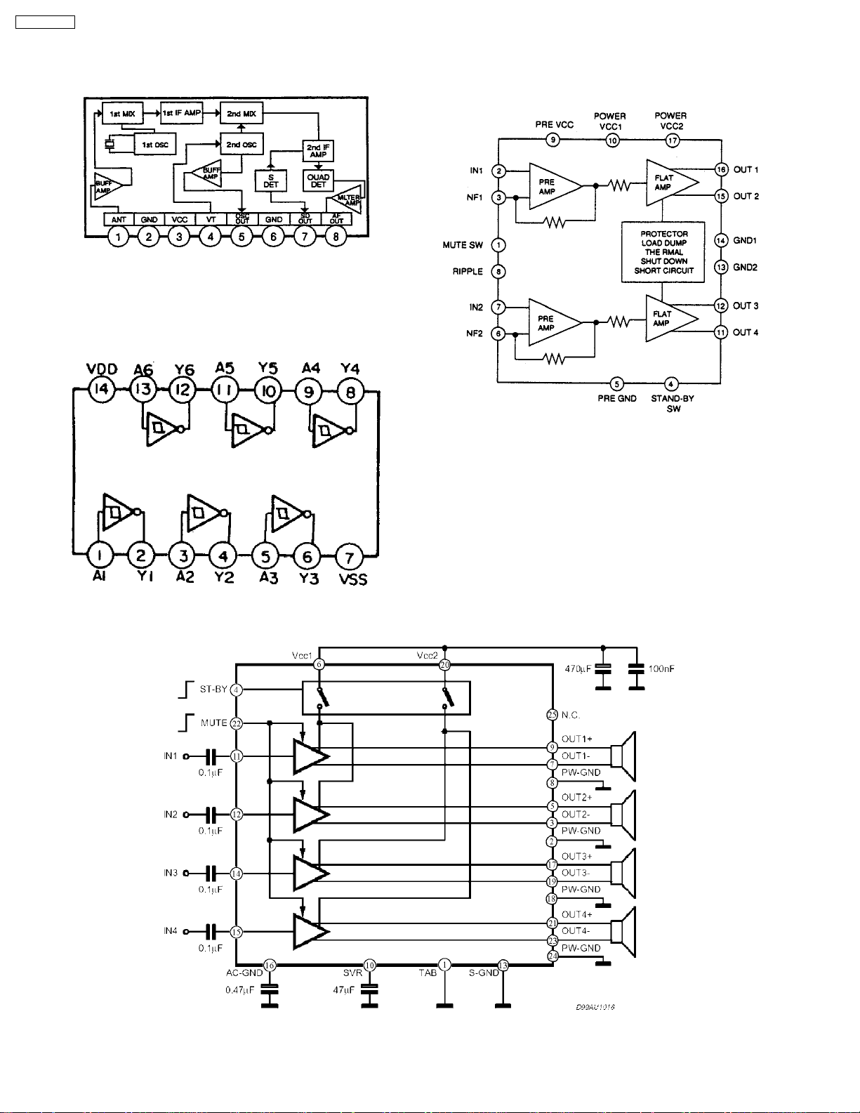
10 PACKAGE AND IC BLOCK DIAGRAM
IC270 C1EA00000041
6
CQ-RG133W1
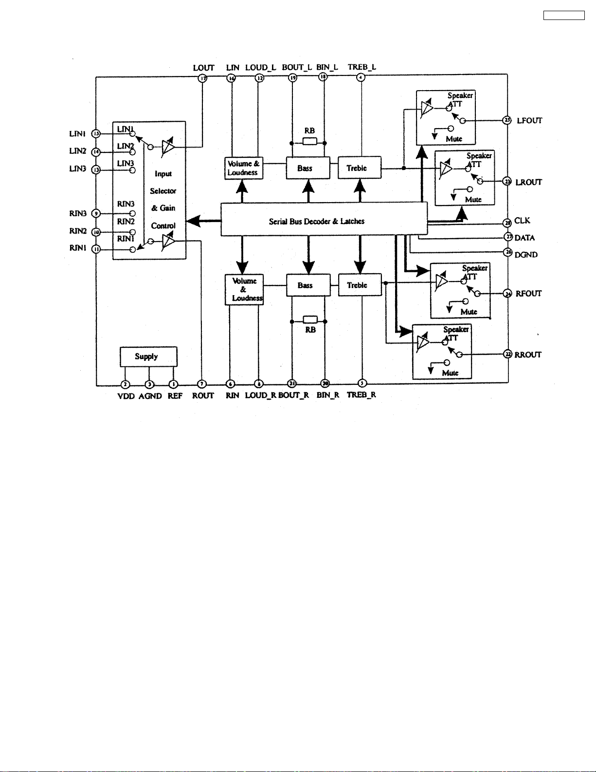
IC205 YEAMPT2313L
7
CQ-RG133W1
 Loading...