


Specifications*
General |
|
Power Supply |
DC 12V (11V - 16V), |
|
Test Voltage 14.4V |
|
Negative Ground |
Tone Controls (Bass/Treble) |
Bass: ±12dB at 60Hz |
|
Treble: ±12dB at 16kHz |
Equalizer Center Frequency |
60, 160, 400, 1k, 3k, 6k, 16k (Hz) |
Variable Range of Equalizer |
-12dB to 12dB (2dB step) |
Current Consumption |
Less than 2.2A |
|
(CD mode; 0.5W × 4-speaker) |
Maximum Power Output |
50W × 4(at 1kHz) |
Speaker Impedance |
4 - 8Ω |
Pre-amp Output Voltage |
|
<CQ-C8413U> |
5V (CD mode; 1kHz, 0dB) |
<CQ-C8313U> |
2.5V (CD mode; 1kHz, 0dB) |
Subwoofer Output Voltage |
|
<CQ-C8413U> |
5V (CD mode; 1kHz, 0dB) |
<CQ-C8313U> |
2.5V (CD mode; 1kHz, 0dB) |
Pre-amp Output Impedance |
|
<CQ-C8413U> |
60Ω |
<CQ-C8313U> |
200Ω |
Subwoofer Output Impedance |
|
<CQ-C8413U> |
60Ω |
<CQ-C8313U> |
200Ω |
FM Stereo Radio |
|
Frequency Range |
87.9MHz - 107.9MHz |
Usable Sensitivity |
10.2dBf. (0.9µV, 75Ω ) |
50dB Quieting Sensitivity |
15.2dBf. (1.6µV, 75Ω ) |
Frequency Response |
30Hz-15kHz (±3dB) |
Alternate Channel Selectivity |
75dB |
ORDER NO. ACED051231C7
C4
AUTOMOTIVE AFTERMARKET
CQ-C8413U
CQ-C8313U
WMA MP3 CD Player/Receiver
Stereo Separation |
35dB (at 1kHz) |
Image Response Ratio |
75dB |
IF Response Ratio |
100dB |
Signal to Noise Ratio |
62dB |
AM Radio |
|
Frequency Range |
530kHz - 1,710kHz |
Usable Sensitivity |
27dB/µV (S/N 20dB) |
CD Player |
|
Sampling Frequency |
8 Times Oversampling |
DA Converter |
4 DAC System |
Pick-up Type |
Astigma 3-Beam |
Light Source |
Semiconductor Laser |
Wave Length |
790 nm |
Frequency Response |
20Hz-20kHz (±1dB) |
Signal to Noise Ratio |
96dB |
Total Harmonic Distortion |
0.01% (1kHz) |
Wow and Flutter |
Below Measurable Limits |
Channel Separation |
75dB |
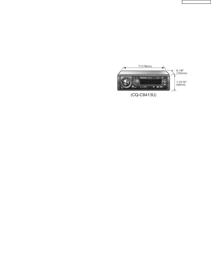
Dimensions (W×H×D)** |
7”×1-15/16”×6-1/8” |
|
(178×50×155mm) |
Weight** |
3 lbs. 8oz (1.6 kg) |
*Specifications and the design are subject to possible modification without notice due to improvements.
**Dimensions and Weight shown are approximate.
**Above specifications comply with EIA standards.
©2005 Matsushita Electric Industrial Co., Ltd. All rights reserved. Unauthorized copying and distribution is a violation of law.

CQ-C8413U / CQ-C8313U
CONTENTS
|
|
Page |
|
|
Page |
1 |
ABOUT LEAD FREE SOLDER (PbF) |
3 |
11 |
IC BLOCK DIAGRAM |
12 |
2 |
FEATUERS |
3 |
12 |
PACKING PARTS LIST |
14 |
3 |
REPLACEING THE FUSE |
3 |
13 |
REPLACEMENT PARTS LIST |
15 |
4 |
MAINTENANCE |
3 |
14 |
EXPLODED VIEW (Unit) |
22 |
5 |
NOTES |
3 |
15 |
CD PLAYER PARTS LIST |
23 |
6 |
DIMENSIONS |
3 |
16 |
EXPLODED VIEW (CD Deck) |
26 |
7 |
LASER PRODUCTS |
3 |
17 |
WIRING DIAGRAM |
27 |
8 |
WIRING CONNECTION |
4 |
18 |
SCHEMATIC DIAGRAM-1 |
32 |
9 |
DISASSEMBLY INSTRUCTIONS |
6 |
19 |
SCHEMATIC DIAGRAM-2 |
33 |
10 |
TERMINALS DESCRIPTION |
9 |
20 |
BLOCK DIAGRAM |
37 |
2
1 ABOUT LEAD FREE
SOLDER (PbF)
Distinction of PbF PCB:
PCBs (manufactured) using lead free solder will have a PbF stamp on the PCB.
Caution :
•Pb free solder has a higher melting point than standard solder; Typically the melting point is 50 - 70°F (30 - 40°C) higher. Please use a soldering iron with temperature control and adjust it to 700 ± 20°F (370 ± 10°C). In case of using high temperature soldering iron, please be careful not to heat too long.
•Pb free solder will tend to splash when heated too high (about 1100°F/600°C)
•This lead free solder will be used for the products after serial No. 1,000,001.
2 FEATUERS
•Hands Free Phone System. (The optional Bluetooth handsfree kit: CY-BT100U)
•Expansion Module (The optional Hub unit: CY-EM100U)
•The optional adapter allows you to connect the optional Panasonic DVD changer unit (CX-DH801U).
•The optional adapter allows you to connect the optional Panasonic CD changer unit (CX-DP880).
•The optional adapter allows you to connect the optional iPod® series.
•XM Satellite Radio. (The optional XM receiver: XMD-1000)
•Sirius Satellite Radio. (The optional Sirius Satellite receiver: SIR-PAN1)
•SQ (Sound Quality).
•SQ7 (7-Band Sound Quality) .
•D.M(Direct Memory)
•Customize the Display (Customize Function)
•MP3/WMA Playback from CD-R/RW.
•This manual is for 2 models CQ-C8413U and CQ-C8313U. The following table describes the differences between 2 models.
3 REPLACEING THE FUSE
Use fuses of the same specified rating 15 amps. Using different substitutes or fuses with higher ratings, or connecting the unit directly without a fuse, could cause fire or damage to the stereo unit.
4 MAINTENANCE
Your products is designed and manufactured to ensure a minimum of maintenance. Use a soft cloth for routine exterior cleaning. Never use benzine, thinner or other solvent.
CQ-C8413U / CQ-C8313U
5 NOTES
[RADIO BLOCK]
Do not align the AM/FM package block. When the package block is necessary, it will be supplied already aligned at the factory.
[CD DECK BLOCK]
This model has no servo alignment points because microcomputer controls the servo circuit
6DIMENSIONS
7LASER PRODUCTS
3
CQ-C8413U / CQ-C8313U
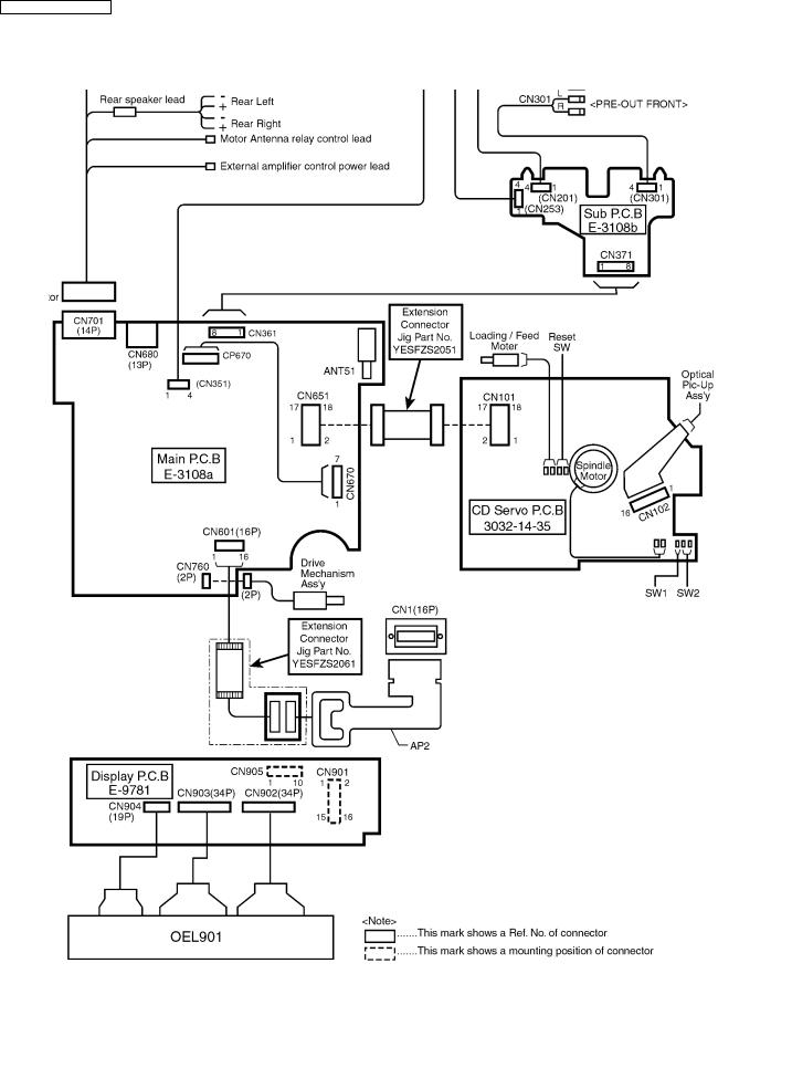
8 WIRING CONNECTION
8.1.CQ-C8413U
4
CQ-C8413U / CQ-C8313U
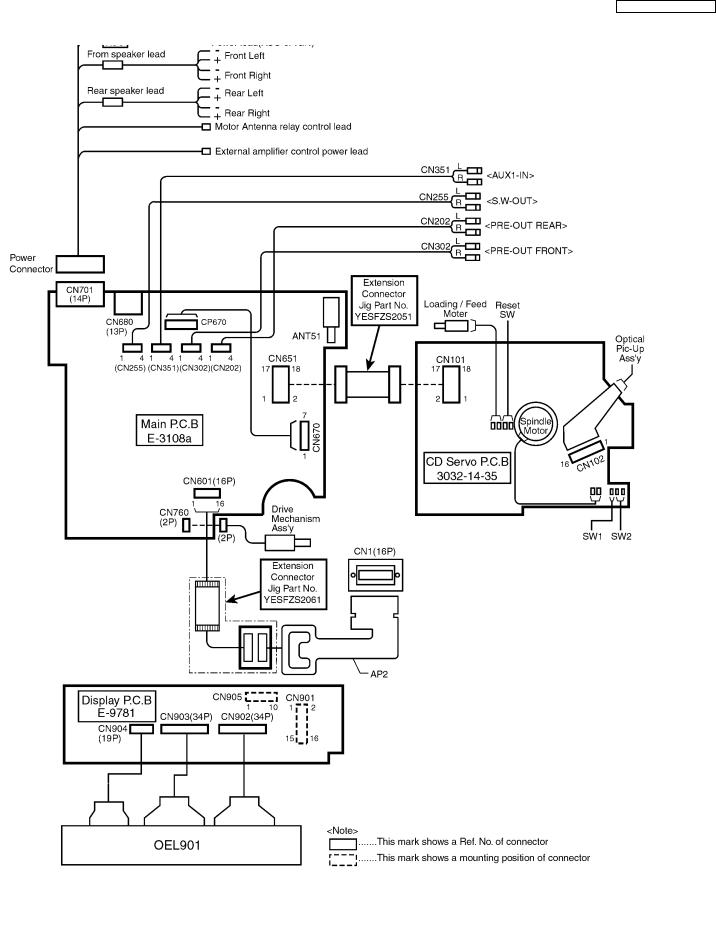
8.2.CQ-C8313U
5

CQ-C8413U / CQ-C8313U
9 DISASSEMBLY INSTRUCTIONS
9.1.How to Remove the Flexible PCB(AP2)
6
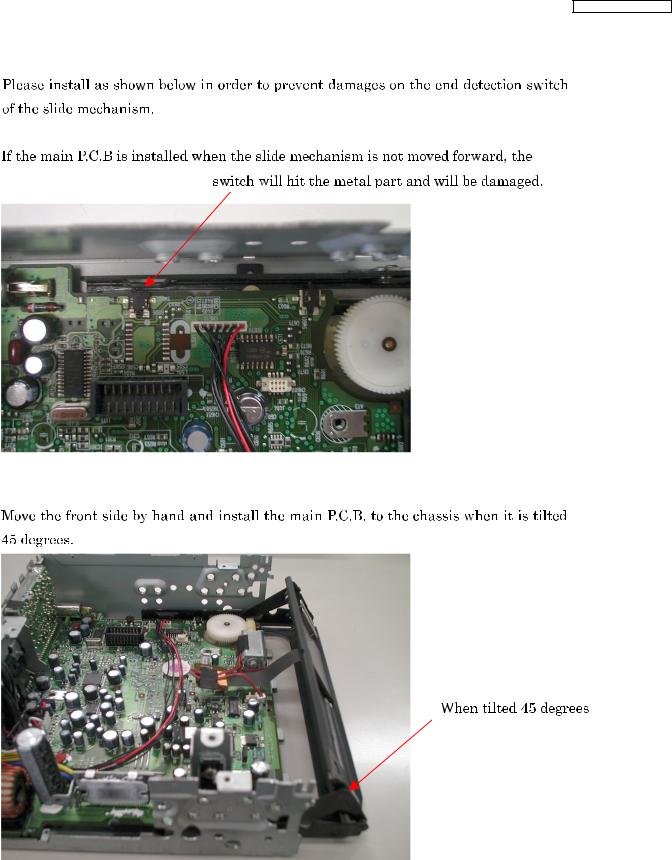
CQ-C8413U / CQ-C8313U
9.2.How to Install the Main P.C.B. of the Electric Display
7

CQ-C8413U / CQ-C8313U
8

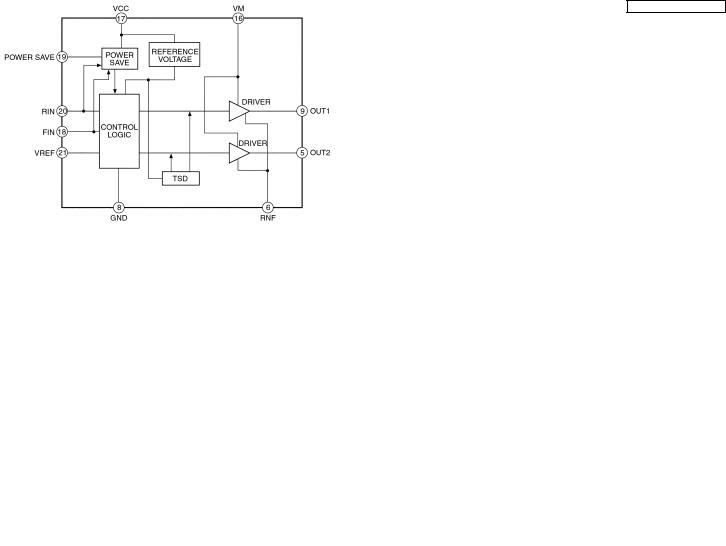
10 TERMINALS DESCRIPTION
10.1. Main Block
IC601 : C2CBKG000034
Pin |
Port |
Description |
(I/O |
|
(V) |
|
No. |
|
|
) |
FM |
AM |
CD |
1 |
PANEL OPEN |
Panel open detection |
I |
0 |
5.2 |
5.2 |
2 |
PANEL |
Panel close detection |
I |
0 |
0 |
5.2 |
|
CLOSE |
|
|
|
|
|
3 |
SUBM CNT |
3.3V power control for |
O |
5.0 |
- |
- |
|
|
Display |
|
|
|
|
4 |
BATT |
Battery power check |
I |
4.8 |
5.0 |
5.0 |
5 |
ACC |
Acc. power check |
I |
4.8 |
5.0 |
5.0 |
6 |
SDA |
Serial data for electronic |
I/O |
4.9 |
4.9 |
4.9 |
|
|
volume |
|
|
|
|
7 |
SCLK |
Serial clock for electronic |
O |
4.9 |
4.9 |
4.9 |
|
|
volume |
|
|
|
|
8 |
CD MUTE |
Signal mute from CD deck |
I |
5.0 |
5.0 |
5.0 |
9 |
Vss |
GND |
- |
0 |
0 |
0 |
10 |
ST |
FM stereo detection |
I |
5.1 |
5.2 |
5.2 |
11 |
PLL DI (MO) |
Serial data to PLL |
O |
0.6 |
0 |
0 |
12 |
PLL DO (MI) |
Serial data from PLL |
I |
5.2 |
5.2 |
5.2 |
13 |
PLL CLK |
Serial clock for PLL |
O |
4.9 |
4.9 |
4.9 |
14 |
PLL CE |
Chip enable for PLL |
O |
0 |
0 |
0 |
15 |
CD RESET |
Reset for CD deck |
O |
4.9 |
4.9 |
4.9 |
16 |
SUB SI |
Serial data to Display CPU |
O |
0.6 |
0.6 |
0.8 |
17 |
CD IN |
Disc-in detection |
I |
5.0 |
5.0 |
5.0 |
18 |
SUB SO |
Serial data from Display |
I |
4.4 |
4.4 |
4.4 |
|
|
CPU |
|
|
|
|
19 |
CH DATA/ UP |
XM SO/UP SO Serial data |
I |
1.6 |
1.6 |
1.6 |
|
SO |
from Changer |
|
|
|
|
20 |
CH CLK/ UP |
Serial clock for Changer or |
I |
4.9 |
4.9 |
4.9 |
|
CLK |
Flash writer |
|
|
|
|
21 |
Vdd |
+5V power supply |
- |
4.9 |
4.9 |
4.9 |
22 |
XM SI (MO)/ |
Serial data to Satellite or |
O |
0 |
0 |
0 |
|
UP SI |
Flash writer |
|
|
|
|
23 |
CD SI (MO) |
Serial data to CD deck |
O |
0 |
0 |
0 |
24 |
CD SCK |
Serial clock for CD deck |
I/O |
0 |
0.4 |
0 |
25 |
CONDENSOR |
Capacitor connection for |
- |
3.3 |
3.3 |
3.3 |
|
|
power |
|
|
|
|
26 |
CD SO (MI) |
Serial data from CD deck |
I |
0 |
0 |
0 |
27 |
CH STB |
Strobe from Changer |
I |
0 |
0 |
0 |
28 |
CH REM OUT |
Remote control codes to |
O |
4.9 |
4.9 |
0.4 |
|
|
Changer |
|
|
|
|
29 |
DECK V |
Power control for CD deck |
O |
4.9 |
4.9 |
4.9 |
|
CONT |
|
|
|
|
|
30 |
REMO INT |
Interrupt for remote control |
I |
3.7 |
3.7 |
3.7 |
31 |
CD FS |
Frame sync. for CD deck |
O |
- |
- |
- |
32 |
Avdd |
+5V power supply |
- |
5.1 |
5.1 |
5.1 |
33 |
AVREF |
+5V power supply |
- |
5.1 |
5.1 |
5.1 |
34 |
AVGND |
GND |
- |
0 |
0 |
0 |
35 |
AVSS |
GND |
- |
0 |
0 |
0 |
36 |
SD |
FM/AM signal level meter |
I |
0.2 |
0 |
0.3 |
37 |
INIT A |
Model setting A by voltage |
I |
0 |
0 |
0 |
|
|
level |
|
|
|
|
38 |
INIT B |
Model setting B by voltage |
I |
0 |
0 |
0 |
|
|
level |
|
|
|
|
39 |
A IN |
Spectrum analyzer data |
I |
0 |
0 |
0 |
40 |
Vss |
GND |
- |
0 |
0 |
0 |
41 |
SYS ID1 |
Hub connection device |
I |
0 |
0 |
0 |
|
|
detection ID 1 |
|
|
|
|
42 |
SYS ID2 |
Hub connection device |
I |
5.2 |
5.2 |
5.2 |
|
|
detection ID 2 |
|
|
|
|
43 |
HUB EVENT |
Bluetooth incoming |
I |
5.2 |
5.2 |
5.2 |
|
|
detection |
|
|
|
|
44 |
HUB CNT |
Request of hub |
O |
0 |
0 |
0 |
|
|
connection check |
|
|
|
|
45 |
CD SW1 |
Disc detection switch 1 |
I |
0 |
0 |
0 |
46 |
CD SW2 |
Disc detection switch 2 |
I |
0 |
0 |
0 |
CQ-C8413U / CQ-C8313U
Pin |
Port |
Description |
(I/O |
|
(V) |
|
No. |
|
|
) |
FM |
AM |
CD |
47 |
MOD0 |
Operating mode control 0 |
I |
5.1 |
5.1 |
5.1 |
|
|
from Flash writer |
|
|
|
|
48 |
MOD1 |
Operating mode control 1: |
- |
5.1 |
5.1 |
5.1 |
|
|
pulled up to H |
|
|
|
|
49 |
MOD2 |
Operating mode control 2 |
I |
0 |
0 |
0 |
|
|
from Flash writer |
|
|
|
|
50 |
H STANDBY |
Standby control from |
I |
5.0 |
5.0 |
5.0 |
|
|
external |
|
|
|
|
51 |
DCDC CONT |
Not connected |
- |
- |
- |
- |
52 |
FP MOTOR1 |
Open/Close of Front panel |
O |
4.9 |
5.0 |
4.9 |
|
|
1 |
|
|
|
|
53 |
FP MOTOR2 |
Open/Close of Front panel |
O |
4.9 |
5.0 |
4.9 |
|
|
2 |
|
|
|
|
54 |
V CONT1 |
Reference voltage control |
O |
0 |
0 |
5.0 |
|
|
for motor driver |
|
|
|
|
55 |
REMO 1 |
Remote control data |
I |
5.0 |
5.0 |
5.0 |
56 |
SA CLK |
Spectrum analyzer clock |
O |
5.0 |
5.0 |
4.9 |
57 |
EXT MUTE |
Pulled up to H |
I |
5.3 |
5.2 |
5.2 |
58 |
AMP CONT |
Power control for external |
O |
4.9 |
5.0 |
4.9 |
|
|
Amplifier |
|
|
|
|
59 |
BZ OUT |
Buzzer signal |
O |
0 |
0 |
0 |
60 |
OEL VCONT |
Power control for OEL |
O |
0 |
0 |
0 |
61 |
WOW MODE1 |
SRS WOW mode 1 |
O |
0 |
0 |
0 |
|
|
(C8403U only) |
|
|
|
|
62 |
WOW MODE2 |
SRS WOW mode 2 |
O |
0 |
0 |
0 |
|
|
(C8403U only) |
|
|
|
|
63 |
WOW MODE3 |
SRS WOW mode 3 |
O |
0 |
0 |
0 |
|
|
(C8403U only) |
|
|
|
|
64 |
DIM1 |
Not connected |
- |
- |
- |
- |
65 |
DIM2 |
Not connected |
- |
- |
- |
- |
66 |
MAIN CNT2 |
Power control for Hub |
O |
5.0 |
5.0 |
5.0 |
67 |
SRC KEY |
SOURCE key detection |
I |
5.0 |
4.9 |
5.0 |
68 |
PANEL IN |
Panel attachment |
I |
- |
- |
- |
|
|
detection |
|
|
|
|
69 |
RDS CLK |
Not connected |
- |
- |
- |
- |
70 |
NC |
Not connected |
- |
- |
- |
- |
71 |
RDS DATA |
Not connected |
- |
- |
- |
- |
72 |
MAIN CONT |
Main power control |
O |
4.9 |
4.9 |
4.9 |
73 |
INV CONT |
Dimmer power control |
O |
5.0 |
5.0 |
5.0 |
74 |
AF MUTE |
Audio mute |
O |
5.0 |
5.0 |
5.0 |
75 |
RESET |
Reset |
I |
5.0 |
5.0 |
5.0 |
76 |
FOCUS ELV |
Focus elevation for SRS |
O |
- |
- |
- |
|
|
WOW (C8403U only) |
|
|
|
|
77 |
X1A |
Oscillator clock |
O |
2.1 |
2.1 |
2.1 |
78 |
X0A |
Oscillator clock |
I |
1.6 |
1.6 |
1.6 |
79 |
Vss |
GND |
- |
0 |
0 |
0 |
80 |
X1 |
Crystal oscillator clock |
I |
2.0 |
2.0 |
2.0 |
81 |
X2 |
Crystal oscillator clock |
O |
2.5 |
2.5 |
2.5 |
82 |
Vdd |
+5V power supply |
- |
5.0 |
5.0 |
5.0 |
83 |
P00 |
Pulled down to L |
- |
0 |
0 |
0 |
84 |
P01 |
Pulled up to H |
- |
5.1 |
5.0 |
5.1 |
85 |
OFFSET DET |
Audio clipping level |
I |
0 |
0 |
0 |
|
|
detection from Power |
|
|
|
|
|
|
amp. |
|
|
|
|
86 |
STBY |
Standby for Power amp. |
O |
5.0 |
5.0 |
5.0 |
87 |
MUTE |
Mute for Power amp. |
O |
0 |
0 |
0 |
88 |
ILL SENS |
Pulled up to H |
- |
5.0 |
5.0 |
5.0 |
89 |
NC |
Not connected |
- |
- |
- |
- |
90 |
EP DO(MI) |
|
|
|
|
|
91 |
NC |
Not connected |
- |
- |
- |
- |
92 |
NC |
Not connected |
- |
- |
- |
- |
93 |
SUB RESET |
Reset for display CPU |
O |
4.9 |
5.0 |
4.9 |
94 |
DISPM CONT |
5V power control for |
O |
0 |
0 |
0 |
|
|
Display |
|
|
|
|
95 |
NC |
Not connected |
- |
- |
- |
- |
96 |
NC |
Not connected |
- |
- |
- |
- |
9

CQ-C8413U / CQ-C8313U
Pin |
Port |
Description |
(I/O |
|
(V) |
|
No. |
|
|
) |
FM |
AM |
CD |
97 |
NC |
Not connected |
- |
- |
- |
- |
98 |
S LED |
Security LED drive |
O |
0 |
0 |
5.0 |
99 |
ANT CONT |
Power control for antenna |
O |
5.2 |
5.2 |
5.2 |
|
|
motor |
|
|
|
|
100 |
NC |
Not connected |
- |
- |
- |
- |
10.2. Display Block
IC901 C2CBKJ000189
Pin |
Port |
Part Name & Description |
I/O |
(V) |
No. |
|
|
|
|
1 |
NC |
Not connected |
- |
- |
2 |
DCLK SLV4 |
Slave D-CLK4 (Clock for |
I |
1.5 |
|
|
image data) |
|
|
3 |
UART SS4 |
GND |
- |
0 |
4 |
UART SS3 |
GND |
- |
0 |
5 |
D DIS |
Disable for Anode drive |
O |
0 |
|
|
(Disable for image signal) |
|
|
6 |
PADJ IO2 |
Anode output pulse width |
O |
3.8 |
|
|
adjusting data 2 (Image data) |
|
|
7 |
DCLK SLV3 |
Slave D-CLK 3 (Clock for |
I |
1.5 |
|
|
image data) |
|
|
8 |
NC |
Not connected |
- |
- |
9 |
NC |
Not connected |
- |
- |
10 |
NC |
Not connected |
- |
- |
11 |
KS1 |
Key scan 1 |
O |
0 |
12 |
KS2 |
Key scan 2 |
O |
0 |
13 |
KS3 |
Key scan 3 |
O |
0 |
14 |
NC |
Not connected |
- |
- |
15 |
BUS BYTE |
GND |
- |
0 |
16 |
CNVSS |
CPU rewrite mode/Single |
I |
0 |
|
|
CPU mode selection for |
|
|
|
|
Flash writer |
|
|
17 |
IADJ |
Anode output current |
O |
0 |
|
|
adjusting data (Luminance |
|
|
|
|
control) |
|
|
18 |
I CLK |
Clock for anode output |
O |
0 |
|
|
current adjusting data |
|
|
19 |
RESET |
Reset from main CPU |
I |
4.4 |
20 |
X1 |
Ceramic oscillator clock |
O |
2.5 |
|
|
(8MHz) |
|
|
21 |
GND |
GND |
- |
0 |
22 |
X0 |
Ceramic oscillator clock |
I |
2.2 |
|
|
(8MHz) |
|
|
23 |
VCC5.0V |
Power supply |
- |
4.6 |
24 |
NMI |
Pulled up to H |
- |
4.6 |
25 |
Y SYNC |
Cathode scan data and |
O |
0 |
|
|
Cathode latch control |
|
|
|
|
(Vertical sync.) |
|
|
26 |
NC |
Not connected |
- |
- |
27 |
NC |
Not connected |
- |
- |
28 |
X SYNC |
Clock for Cathode scan; or |
O |
0 |
|
|
Latch strobe for Anode |
|
|
|
|
output pulse width adjusting |
|
|
|
|
data and Anode output |
|
|
|
|
current adjusting data |
|
|
29 |
A CLK TA |
Anode output pulse width |
O |
2.7 |
|
|
adjusting clock |
|
|
30 |
NC |
Not connected |
- |
- |
31 |
NC |
Not connected |
- |
- |
32 |
S DIS |
Disable for Cathode drive |
O |
2.4 |
33 |
NC |
Not connected |
- |
- |
34 |
NC |
Not connected |
- |
- |
35 |
NC |
Not connected |
- |
- |
36 |
NC |
Not connected |
- |
- |
37 |
NC |
Not connected |
- |
- |
Pin |
Port |
Part Name & Description |
I/O |
(V) |
No. |
|
|
|
|
38 |
PADJ IO1/TXD |
Anode output pulse width |
O |
1.2 |
|
|
adjusting data 0 (Image |
|
|
|
|
data); or Serial data for Flash |
|
|
|
|
writer |
|
|
39 |
VCC5.0V |
Power supply |
- |
3.3 |
40 |
RXD |
Serial data from Flash writer |
I |
1.3 |
41 |
GND |
GND |
- |
0 |
42 |
DCLK MST/SCLK |
Master D-CLK (Clock for |
O/I |
3.3 |
|
|
image data);or Serial clock |
|
|
|
|
from Flash writer |
|
|
43 |
BUSY |
Busy for Flash writer |
O |
1.5 |
44 |
OEL OE |
OEL output enable |
O |
0 |
45 |
PADJ IO0 |
Anode output pulse width |
O |
1.8 |
|
|
adjusting data 0 (Image data) |
|
|
46 |
DCLK SLV0 |
Slave D-CLK 0 (Clock for |
I |
2.7 |
|
|
image data) |
|
|
47 |
UART SS0 |
GND |
- |
0 |
48 |
NC |
Not connected |
- |
- |
49 |
FLASH CE |
Chip enable for Flash |
O |
1.7 |
|
|
memory |
|
|
50 |
NC |
Not connected |
- |
- |
51 |
NC |
Not connected |
- |
- |
52 |
RY/BY |
Pulled up to H |
- |
3.6 |
53 |
NC |
Not connected |
- |
- |
54 |
EPM |
Program mode enable for |
I |
2.3 |
|
|
Flash writer |
|
|
55 |
NC |
Not connected |
- |
- |
56 |
NC |
Not connected |
- |
- |
57 |
GND |
GND |
- |
0 |
58 |
NC |
Not connected |
- |
- |
59 |
VCC3.3V |
Power supply |
- |
3.6 |
60 |
NC |
Not connected |
- |
- |
61 |
NC |
Not connected |
- |
- |
62 |
NC |
Not connected |
- |
- |
63 |
FLASH OE |
Output enable for Flash |
O |
3.6 |
|
|
memory |
|
|
64 |
NC |
Not connected |
- |
- |
65 |
FLASH WE |
Write enable for Flash |
O |
3.6 |
|
|
memory |
|
|
66 |
NC |
Not connected |
- |
- |
67 |
NC |
Not connected |
- |
- |
68 |
NC |
Not connected |
- |
- |
69 |
NC |
Not connected |
- |
- |
70 |
FLASH A22 |
A22 in Address bus |
O |
0 |
71 |
FLASH A21 |
A21 in Address bus |
O |
3.6 |
72 |
FLASH A20 |
A20 in Address bus |
O |
3.6 |
73 |
FLASH A19 |
A19 in Address bus |
O |
0 |
74 |
VCC3.3V |
Power supply |
- |
3.6 |
75 |
FLASH A18 |
A18 in Address bus |
O |
3.6 |
76 |
GND |
GND |
- |
0 |
77 |
FLASH A17 |
A17 in Address bus |
O |
0 |
78 |
FLASH A16 |
A16 in Address bus |
O |
2.5 |
79 |
FLASH A15 |
A15 in Address bus |
O |
0 |
80 |
FLASH A14 |
A14 in Address bus |
O |
0 |
81 |
FLASH A13 |
A13 in Address bus |
O |
2.5 |
82 |
FLASH A12 |
A12 in Address bus |
O |
2.5 |
83 |
FLASH A11 |
A11 in Address bus |
O |
0 |
84 |
FLASH A10 |
A10 in Address bus |
O |
0 |
85 |
FLASH A9 |
A9 in Address bus |
O |
0 |
86 |
FLASH WP |
Write protect/Accelaration |
O |
0 |
|
|
from Flash memory |
|
|
87 |
NC |
Not connected |
- |
- |
88 |
NC |
Not connected |
- |
- |
89 |
NC |
Not connected |
- |
- |
90 |
NC |
Not connected |
- |
- |
91 |
VDD 3.3V |
Power supply |
- |
3.4 |
92 |
FLASH A8 |
A8 in Address bus |
O |
0 |
93 |
GND |
GND |
- |
0 |
10
Pin |
Port |
Part Name & Description |
I/O |
(V) |
No. |
|
|
|
|
94 |
FLASH A7 |
A7 in Address bus |
O |
0 |
95 |
FLASH A6 |
A6 in Address bus |
O |
0 |
96 |
FLASH A5 |
A5 in Address bus |
O |
0.6 |
97 |
FLASH A4 |
A4 in Address bus |
O |
3.0 |
98 |
FLASH A3 |
A3 in Address bus |
O |
1.8 |
99 |
FLASH A2 |
A2 in Address bus |
O |
1.8 |
100 |
FLASH A1 |
A1 in Address bus |
O |
1.8 |
101 |
FLASH A0 |
Not connected |
- |
- |
102 |
FLASH D15 |
DQ15 in Data bus |
I/O |
3.1 |
103 |
FLASH D14 |
DQ14 in Data bus |
I/O |
0.6 |
104 |
FLASH D13 |
DQ13 in Data bus |
I/O |
0.4 |
105 |
FLASH D12 |
DQ12 in Data bus |
I/O |
0.4 |
106 |
FLASH D11 |
DQ11 in Data bus |
I/O |
0.4 |
107 |
FLASH D10 |
DQ10 in Data bus |
I/O |
0.4 |
108 |
FLASH D9 |
DQ9 in Data bus |
I/O |
0.7 |
109 |
FLASH D8 |
DQ8 in Data bus |
I/O |
1.6 |
110 |
FLASH D7 |
DQ7 in Data bus |
I/O |
1.7 |
111 |
FLASH D6 |
DQ6 in Data bus |
I/O |
1.6 |
112 |
FLASH D5 |
DQ5 in Data bus |
I/O |
1.6 |
113 |
FLASH D4 |
DQ4 in Data bus |
I/O |
1.6 |
114 |
FLASH RESET |
Reset for Flash memory |
O |
3.4 |
115 |
NC |
Not connected |
- |
- |
116 |
NC |
Not connected |
- |
- |
117 |
NC |
Not connected |
- |
- |
118 |
NC |
Not connected |
- |
- |
119 |
FLASH D3 |
DQ3 in Data bus |
I/O |
0 |
120 |
FLASH D2 |
DQ2 in Data bus |
I/O |
1.8 |
121 |
FLASH D1 |
DQ1 in Data bus |
I/O |
2.3 |
122 |
FLASH D0 |
DQ0 in Data bus |
I/O |
2.2 |
123 |
NC |
Not connected |
- |
- |
124 |
NC |
Not connected |
- |
- |
125 |
SUB SI |
Serial data from main CPU |
I |
0 |
126 |
SUB SO |
Serial data to main CPU |
O |
0.8 |
127 |
ROTARY 1 |
Volume-up detection from |
I |
1.8 |
|
|
Rotary encoder |
|
|
128 |
ROTARY 2 |
Volume-down detection from |
I |
4.5 |
|
|
Rotary encoder |
|
|
129 |
A CLK SCLK |
Anode output pulse width |
I |
2.6 |
|
|
adjusting clock |
|
|
130 |
GND |
GND |
- |
0 |
131 |
A CLK |
Anode output pulse width |
O |
0.7 |
|
|
adjusting clock |
|
|
132 |
VCC5.0V |
Power supply |
- |
4.5 |
133 |
KEY RET4 |
Key return 4 |
I |
0 |
134 |
KEY RET3 |
Key return 3 |
I |
0 |
135 |
KEY RET2 |
Key return 2 |
I |
0 |
136 |
KEY RET1 |
Key return 1 |
I |
0 |
137 |
OEL RESET |
Reset for OEL |
O |
4.5 |
138 |
NC |
Not connected |
- |
- |
139 |
NC |
Not connected |
- |
- |
140 |
AD AVSS |
GND |
- |
0 |
141 |
TH DETECT |
Thermal detection |
I |
1.7 |
142 |
AD VREF |
+5V Power supply |
- |
4.5 |
143 |
AD AVCC |
+5V Power supply |
- |
4.5 |
144 |
PADJ IO3 |
Anode output pulse width |
O |
1.2 |
|
|
adjusting data 3 (Image data) |
|
|
|
|
|
CQ-C8413U / CQ-C8313U |
|||
10.3. |
CD Servo Block |
|
|
|
|
|
IC101 : YESAM337 |
|
|
|
|
|
|
|
|
|
|
|
|
|
Pin No. |
Port |
Descriptions |
|
I/O |
(V) |
|
1 |
AVSS |
GND |
|
- |
0 |
|
2 |
LD-MT |
Loading Motor drive IC control 1 |
|
O |
3.2 |
|
3 |
CNT |
Loading Motor drive IC control 2 |
|
O |
3.2 |
|
4 |
- |
- |
|
- |
- |
|
5 |
LD-EJ |
Loading Motor drive IC control |
|
O |
0 |
|
|
|
(Eject) |
|
|
|
|
6 |
AMUTE |
Mute signal output |
|
O |
0 |
|
7 |
- |
- |
|
- |
- |
|
8 |
SBSY |
DSP IC SBSY |
|
O |
0 |
|
9 |
- |
- |
|
- |
- |
|
10 |
- |
- |
|
- |
- |
|
11 |
TXD0 |
Serial data output |
|
O |
0 |
|
12 |
RXD0 |
Serial data input |
|
I |
0 |
|
13 |
CLK0 |
Clock input |
|
I |
2.9 |
|
14 |
- |
- |
|
- |
- |
|
15 |
- |
- |
|
- |
- |
|
16 |
- |
- |
|
- |
- |
|
17 |
AMD |
- |
|
- |
3.2 |
|
18 |
DVCC |
Power supply (3.3V) |
|
- |
3.2 |
|
19 |
X2 |
Crystal oscillator |
|
- |
1.3 |
|
20 |
DVSS |
GND |
|
- |
0 |
|
21 |
X1 |
Crystal oscillator |
|
- |
1.3 |
|
22 |
AMI |
- |
|
- |
3.2 |
|
23 |
RESET |
Reset |
|
I |
3 |
|
24 |
- |
- |
|
- |
- |
|
25 |
- |
- |
|
- |
- |
|
26 |
NMI |
- |
|
- |
3.2 |
|
27 |
- |
- |
|
- |
- |
|
28 |
STBY |
DSP IC STBY |
|
O |
0 |
|
29 |
RST |
DSP IC RST |
|
O |
3.2 |
|
30 |
CCE |
DSP IC CCE |
|
O |
2.6 |
|
31 |
BUCK |
DSP IC CK |
|
O |
2.8 |
|
32 |
BUS3 |
DSP IC BUS3 |
|
O |
2.8 |
|
33 |
BUS2 |
DSP IC BUS2 |
|
O |
2.8 |
|
34 |
BUS1 |
DSP IC BUS1 |
|
O |
2.8 |
|
35 |
BUS0 |
DSP IC BUS0 |
|
O |
2.9 |
|
36 |
RESET SW |
Mechanics deck REST SW input |
|
I |
3.2 |
|
37 |
SW1 |
Mechanics deck SW1 input |
|
I |
0 |
|
38 |
SW2 |
Mechanics deck SW2 input |
|
I |
0 |
|
39 |
CONT (P13) |
DSP IC power control 1 |
|
O |
3.2 |
|
40 |
- |
- |
|
- |
- |
|
41 |
- |
- |
|
- |
- |
|
42 |
- |
- |
|
- |
- |
|
43 |
CONT (P17) |
DSP IC power control 2 |
|
O |
3.2 |
|
44 |
PIO0 |
DSP IC PIO0 |
|
O |
0 |
|
45 |
ZDET |
LOAD detect |
|
I |
0 |
|
46-49 |
- |
- |
|
- |
- |
|
50 |
- |
- |
|
- |
3.2 |
|
51-58 |
- |
- |
|
- |
- |
|
59 |
CDFS |
Serial frame sink signal input |
|
I |
2.3 |
|
|
|
(CD ON) |
|
|
|
|
60 |
P50/AN0 |
Reference voltage |
|
I |
0.3 |
|
61 |
P51/AN0 |
Loading motor detect |
|
I |
2.1 |
|
62 |
P52/AN2 |
- |
|
- |
0 |
|
63 |
P53/AN3 |
- |
|
- |
0 |
|
64 |
AVCC |
Power supply (3.3V) |
|
- |
3.2 |
|
11

CQ-C8413U / CQ-C8313U
11 IC BLOCK DIAGRAM
11.1. Main Block
IC670 : C0JBAZ000904
IC701 : C0DAZHF00004
IC201 : C1BB00000796
IC730 : C0DAEKG00002
IC231 : C0JBZS000003 [CQ-C8413U]
IC755 : C0DBZGD00040
12
CQ-C8413U / CQ-C8313U
11.2. CD Servo Block
IC401,403 : YESAM341
IC760 : C0GBG0000032
IC402 : YESAM342
IC770 : C0DBAHG00020
13
CQ-C8413U / CQ-C8313U
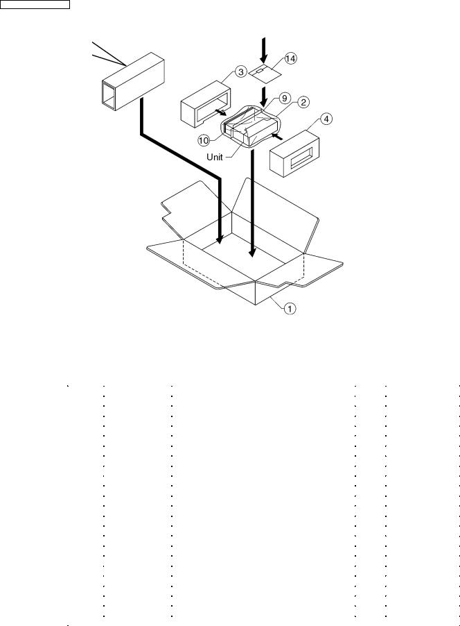
12 PACKING PARTS LIST
· Item numbers listed below should not order regular spare parts. (not available)
Item No. |
Part No. |
Part Name & Description |
Q´ty |
Remarks |
1 |
- |
Inner Carton |
1 |
Not available |
2 |
- |
Polyethylene Bag |
1 |
Not available |
3 |
- |
Packing Pad Front |
1 |
Not available |
4 |
- |
Packing Pad Rear |
1 |
Not available |
5 |
- |
Instruction Kit |
1 |
Not available |
|
- |
Operating Instructions |
(1) |
Not available |
|
- |
System Upgrade Guidebook |
(1) |
Not available |
|
- |
Installation Instructions |
(1) |
Not available |
|
- |
Owners Infomation Card |
(1) |
Not available |
6 |
- |
Sleeve |
1 |
Not available |
7 |
EUR7641010 |
Remote Control Unit (including a battery) |
1 |
|
- |
CR2025/1F |
Lithium Battery |
(1) |
|
8 |
YGAJ021009 |
Power Connector |
1 |
|
9 |
YEFX0217314 |
Mounting Collar |
1 |
|
10 |
YEFC051013 |
Trim Plate |
1 |
|
11 |
YEP0FZ5739 |
Installation kit |
1 |
|
|
- |
Lock Cancel Plate |
(2) |
Not available |
|
- |
Mounting Bolt |
(1) |
Not available |
|
- |
Tapping Screw |
(1) |
Not available |
|
- |
Hex. Nut |
(1) |
Not available |
12 |
YEFG04026 |
Rear Support Strap |
1 |
|
13 |
YEFA134145 |
Removable Face Plate Case |
1 |
|
14 |
YEP0FZ5738 |
Security Screw Kit |
1 |
|
14

13 REPLACEMENT PARTS LIST
Notes :
1.Be sure to make your orders of replacement parts according to this list.
2.Important safety notice: Components, identified by  mark have special characteristics important for safety. When replacing any of these components, use only manufacturer´s specified parts.
3.Location keys in the remarks column indicates the general location of the parts shown in the exploded drawing, as in a road map.
4.The marking (RTL) indicates that Retention Time is limited for this item. After the discontinuation of assembly in production, the item will continue to be available for a specific period of time. The retention period of availability is dependent on the type of assembly, and in accordance with the laws governing part and product retention. After the end of this period, the assembly will no longer be available.
5.“T” marks in remarks colum are indicated supply parts of PTW.
6.Reference materials of parts with the “TSN“ mark in the remarks column are uploaded in the TSN (Technical Service Navigation) system website. Please download from that website for references.
7."A" or "B" marks in remarks column are indicated as follows :
•A : CQ-C8413U
•B : CQ-C8313U
Ref. No. |
Part No. |
Part Name & Description |
Remarks |
[E3108] Main Block |
|
|
|
IC´s AND TRANSISTORs |
|
|
|
IC201 |
C1BB00000796 |
IC |
T |
IC221 |
C1BB00001131 |
IC |
T, A |
IC231 |
C0JBZS000003 |
IC |
T, A |
IC251 |
C0ABBA000221 |
IC |
T, A |
IC252 |
C0ABCA000121 |
IC |
T, A |
IC271 |
C1ZAZ0001450 |
IC |
T |
IC401 |
YEAMLC72146T |
IC |
T |
IC601 |
C2CBKG000034 |
IC |
T |
IC650 |
C0JBAA000372 |
IC |
T |
IC670 |
C0JBAZ000904 |
IC |
T |
IC701 |
C0DAZHF00004 |
IC |
T |
IC702 |
C0EBZ0000035 |
IC |
T |
IC730 |
C0DAEKG00002 |
IC |
T |
IC752 |
C0CBCBG00012 |
IC |
T |
IC755 |
C0DBZGD00040 |
IC |
T |
IC760 |
C0GBG0000032 |
IC |
T |
IC770 |
C0DBAHG00020 |
IC |
T |
IC790 |
C0CBCYG00004 |
IC |
T |
PA51 |
C5BA00000122 |
Electronic Tuner |
T |
Q55 |
B1GDGFEH0001 |
Transistor |
T |
Q56 |
B1AAEC000002 |
Transistor |
T |
Q220 |
B1GBCFNN0004 |
Transistor |
T |
Q235 |
B1GBHBEA0004 |
Transistor |
T |
Q241 |
B1GBHBEA0004 |
Transistor |
T |
Q251 |
B1GBHBEA0004 |
Transistor |
T, A |
Q252 |
B1GBHBEA0004 |
Transistor |
T, A |
Q320 |
B1GBCFNN0004 |
Transistor |
T |
Q335 |
B1GBHBEA0004 |
Transistor |
T |
Q341 |
B1GBHBEA0004 |
Transistor |
T |
Q346 |
B1GBHBEA0004 |
Transistor |
T, B |
Q351 |
B1GBHBEA0004 |
Transistor |
T, A |
Q352 |
B1GBHBEA0004 |
Transistor |
T, A |
|
|
|
CQ-C8413U / CQ-C8313U |
||
|
|
|
|
|
|
Ref. No. |
Part No. |
Part Name & Description |
|
Remarks |
|
Q353 |
B1GBHBEA0004 |
Transistor |
|
T, A |
|
Q354 |
B1GDCFJJ0002 |
Transistor |
|
T, A |
|
Q371 |
B1GBCFNN0004 |
Transistor |
|
T, A |
|
Q372 |
B1GBCFJN0004 |
Transistor |
|
T |
|
Q376 |
B1GBCFNN0004 |
Transistor |
|
T |
|
Q411 |
B1DFBF000001 |
Transistor |
|
T |
|
Q630 |
B1GBCFNN0004 |
Transistor |
|
T |
|
Q633 |
B1GDCFJJ0002 |
Transistor |
|
T |
|
Q650 |
B1GBCFJN0004 |
Transistor |
|
T |
|
Q651 |
B1GBCFJN0004 |
Transistor |
|
T |
|
Q652 |
B1GBCFJN0004 |
Transistor |
|
T |
|
Q680 |
B1GDGFEH0001 |
Transistor |
|
T |
|
Q681 |
B1GDCFJJ0002 |
Transistor |
|
T |
|
Q701 |
B1BACF000026 |
Transistor |
|
T |
|
Q760 |
B1GBCFNN0004 |
Transistor |
|
T |
|
Q771 |
B1ABCF000187 |
Transistor |
|
T, A |
|
Q791 |
B1GBNCEJ0003 |
Transistor |
|
T |
|
Q793 |
B1GBCFJN0004 |
Transistor |
|
T |
|
|
|
|
|
|
|
|
|
|
|
|
|
DIODEs |
|
|
|
|
|
D201 |
B0JCME000012 |
Diode |
|
T |
|
D202 |
B0JCME000012 |
Diode |
|
T |
|
D203 |
B0JCME000012 |
Diode |
|
T |
|
D204 |
B0JCME000012 |
Diode |
|
T |
|
D251 |
B0JCMC000004 |
Diode |
|
T, A |
|
D301 |
B0JCME000012 |
Diode |
|
T |
|
D302 |
B0JCME000012 |
Diode |
|
T |
|
D303 |
B0JCME000012 |
Diode |
|
T |
|
D304 |
B0JCME000012 |
Diode |
|
T |
|
D346 |
B0JCMC000004 |
Diode |
|
T, B |
|
D601 |
B0JCMC000004 |
Diode |
|
T |
|
D630 |
B3AAB0000143 |
Diode |
|
T |
|
D631 |
YEADUDZS56BT |
Diode |
|
T |
|
D632 |
MA3X152D0L |
Diode |
|
T |
|
D635 |
YEADUDZS56BT |
Diode |
|
T |
|
D636 |
YEADUDZS56BT |
Diode |
|
T |
|
D637 |
YEADUDZS56BT |
Diode |
|
T |
|
D638 |
YEADUDZS56BT |
Diode |
|
T |
|
D639 |
YEADUDZS56BT |
Diode |
|
T |
|
D670 |
B0JCMC000004 |
Diode |
|
T |
|
D672 |
B0JCMC000004 |
Diode |
|
T |
|
D673 |
B0BC5R000020 |
Diode |
|
T |
|
D701 |
B0BA04700003 |
Diode |
|
T |
|
D702 |
MA2Q73600L |
Diode |
|
T |
|
D703 |
B0BC5R7A0062 |
Diode |
|
T |
|
D704 |
B0JCMC000004 |
Diode |
|
T |
|
D705 |
B0ECKP000002 |
Diode |
|
T |
|
D706 |
B0ECKP000002 |
Diode |
|
T |
|
D707 |
B0JCPE000004 |
Diode |
|
T |
|
D708 |
MA2Q73600L |
Diode |
|
T |
|
D710 |
B0JCMC000004 |
Diode |
|
T |
|
D715 |
MA3X152A0L |
Diode |
|
T |
|
D716 |
MA3X72100L |
Diode |
|
T |
|
D751 |
B0ECKP000002 |
Diode |
|
T |
|
D752 |
B0ECKP000002 |
Diode |
|
T |
|
D760 |
B0BC5R000020 |
Diode |
|
T |
|
D761 |
B0BC3R0A0058 |
Diode |
|
T |
|
D770 |
B0JCMC000004 |
Diode |
|
T, A |
|
D771 |
B0JCQD000002 |
Diode |
|
T |
|
D772 |
B0BC013A0063 |
Diode |
|
T, A |
|
|
|
|
|
|
|
|
|
|
|
|
|
CAPACITORs |
|
|
|
|
|
C52 |
F1J1H470A025 |
Ceramic, 47PF 50WV |
|
T |
|
C53 |
F1J1H103A513 |
Ceramic, 0.01µF 50WV |
|
T |
|
C54 |
F2A1A221A449 |
Electrolytic, 220µF 10WV |
|
T |
|
C55 |
F1J1H103A513 |
Ceramic, 0.01µF 50WV |
|
T |
|
C56 |
F3F1E105A001 |
Tantalum, 1µF 25WV |
|
T |
|
C57 |
F2A1A101A450 |
Electrolytic, 100µF 10WV |
|
T |
|
C61 |
F1J1E273A002 |
Ceramic, 0.027µF 25WV |
|
T |
|
C62 |
F1J1E273A002 |
Ceramic, 0.027µF 25WV |
|
T |
|
C65 |
F1J1H1020024 |
Ceramic, 1000PF 50WV |
|
T |
|
C206 |
F2A1C100A502 |
Electrolytic, 10µF 16WV |
|
T |
|
15
 Loading...