


 Loading...
CD RECEIVER
KDC-MP225 KDC-MP4026/G KDC-W4527/G/GY/Y KDC-W427Y
SERVICE MANUAL
© 2003-12 PRINTED IN JAPAN B53-0113-00 (N) 2704
CD mechanism extension cord (24PIN) : W05-0934-00
Panel assy
KDC-MP225 (A64-3170-02)
|
Panel assy |
Front glass |
Front glass |
KDC-W4527/Y (A64-3172-02) |
KDC-W4527/Y (B10-4466-01) |
KDC-MP225 (B10-4464-01) |
KDC-W4527G/GY(A64-3173-02) |
KDC-W4527G/GY(B10-4467-01) |
- |
SCRL |
C.S. + |
- |
SCRL |
PTY + |
UD |
UD |
LO |
LO |
|
AUD |
OFF |
SCAN |
RDM |
REP |
F.SEL |
M.RDM DISP MENU |
|
AUD |
OFF |
SCAN |
RDM |
REP |
F.SEL |
M.RDM DISP MENU |
AME |
AUTO |
|
|
|
|
|
|
TI |
VOL |
|
|
|
|
|
|
|
|
|
|
|
|
ADJ |
|
|
|
|
|
|
Panel assy
KDC-MP4026 (A64-3174-02) KDC-MP4026G(A64-3175-02)
Front glass |
|
Front glass |
KDC-MP4026 (B10-4468-01) |
Panel assy |
|
KDC-MP4026G(B10-4469-01) |
KDC-W427 (A64-3336-02) |
KDC-W427 (B10-4555-01) |
- |
SCRL |
+ |
SCRL |
UD |
UD |
LO |
LO |
|
AUD |
OFF |
SCAN |
RDM |
REP |
F.SEL |
M.RDM DISP MENU |
|
AUD |
OFF |
SCAN |
RDM |
REP |
F.SEL |
DISP MENU |
AME |
AUTO |
|
|
|
|
|
|
AME |
AUTO |
|
|
|
|
|
|
* DC cord |
* DC cord |
* Antenna adaptor |
* Screw set |
* Screw |
Lever |
(E30-6322-05) |
(E30-6132-05) |
(T90-0523-05) |
(N99-1719-05) |
(N84-4016-46) |
(D10-4589-04) x 2 |
(E30-6323-05) |
(E30-6286-05) |
|
|
|
|
* Escutcheon |
Mounting hardware assy |
(B07-3001-02) |
(J21-9716-03) |
(B07-3098-02) |
|
* Depends on model. Refer to the parts list.
Plastic cabinet assy |
* Remote controller assy |
(A02-1486-13) |
(A70-2040-05) : RC-505 |
* Not supplied
TDF PANEL INFORMATION
MODEL PARTS NO. PANEL NAME
KDC-MP225 Y33-1940-60 TDF-42D
KDC-MP4026 Y33-1940-67 TDF-MP4026
KDC-MP4026G Y33-1940-63 TDF-MP4026G
KDC-W4527/Y Y33-1940-64 TDF-W4527
KDC-W4527G/GY Y33-1940-65 TDF-W4527G
KDC-W427Y Y33-1940-66 TDF-W427Y
2
CD PLAYER UNIT (X32-5500-00) |
|
|
|
|
|
|
|||
CN1 |
|
|
|
|
|
|
|
|
|
DOUT |
24 OPEN |
|
IC1 |
|
|
|
IC3 |
|
|
|
|
S2 |
Q1,4 |
|
|
|
|
||
12EJE |
|
|
|
|
|
4 |
|
||
|
|
|
|
8 |
|
|
|||
|
|
LEVEL |
|
|
|
MP3/WMA |
|
||
|
|
|
|
|
|
|
|||
|
|
|
|
|
|
|
|
||
|
|
|
|
|
|
|
DECODER |
|
|
|
|
S1 |
SHIFT |
|
|
|
16.00MHz |
|
|
|
|
|
|
|
|
|
|||
LOS |
|
|
MICROPROCESSOR |
X2 |
|
|
|
||
|
|
|
|
IC8 |
|
||||
|
|
|
MECHANISM |
|
|
|
|
||
|
|
|
|
|
|
|
|
||
CLK |
|
|
|
CONTROL |
|
|
|
BUFFER |
|
DATA |
20 |
IC9 |
|
|
|
|
|
Q9,10 |
|
|
|
|
|
|
|
||||
|
|
|
|
|
|
|
|
||
A8V |
|
A8V |
DAC 3.3V |
A3.3V |
|
|
AVR |
|
|
L |
|
|
|
|
|
|
|
|
|
AGND |
|
|
|
|
R |
|
|
Q3,5,6 |
|
|
|
|
|
|
MUTER |
15 |
3 |
LEVEL |
|
MUTEL |
|
|||
|
|
SHIFT |
|
|
MRST |
|
|
|
|
|
|
|
|
|
MSTOP |
|
(0-01)ONLY |
|
|
|
|
|
||
8EJE |
|
S4 |
Q7 |
|
|
|
|||
|
|
|
||
|
|
|
|
LEVEL SHIFT |
LOE/LIM |
10 |
S3 |
|
|
|
|
|
||
|
1 |
|
|
|
C-SW |
|
|
|
|
|
|
BU3.3V |
|
IC2 |
|
|
|
|
|
|
RF AMP/SERVO |
5 |
|
|
|
|
CD SIGNAL |
|
|
|
|
|
|
|
|
|
3 |
|
PROCESSOR |
|
|
IC6 |
IC7 |
BU2.5V |
X1 |
Q8 |
VREF |
|
|
||||
BU 3.3V |
DAC 3.3V |
|
|
|
|
|
16.898MHz |
APC |
|||
AVR |
AVR |
|
|||
|
|
||||
BU5 |
|
BU5V |
|
|
|
|
|
|
|
|
|
|
|
|
4 |
|
|
DGND |
|
|
|
|
|
|
|
|
|
|
IC5 |
|
|
|
|
|
|
DGND |
|
|
|
SW3.3V |
|
|
|
|
|
|
|
|
|
|
|
||
D5 |
|
D5V |
SW 3.3V |
|
|
|
|
|
|
|
|
|
|
|
|||
D5 |
5 |
|
AVR |
|
PON |
IC4 |
|
|
|
|
|
|
|
FCS |
|||
LO/EJ |
|
|
|
|
|
|||
|
|
|
|
|
4 |
|||
|
|
|
|
|
|
TRK |
||
|
|
2 |
|
|
|
|
||
MOTOR |
|
|
|
|
4ch BTL |
|
SPD |
|
|
|
|
S7V |
|
|
|||
S7V |
|
|
|
|
DRIVER |
4 |
SLD |
|
|
|
|
|
|
||||
|
|
|
|
|
|
|
||
SGND |
1 |
|
|
|
|
|
|
|
CN2
DM1 M
DM2 M
DPU1 |
|
(OPTICAL PICKUP) |
|
|
LD |
|
PD |
|
E |
16 |
A B |
|
|
|
C |
|
F |
TR COIL |
|
FO COIL |
|
SPINDLE |
|
MOTOR |
|
LOADING |
|
& SLED |
|
MOTOR |
|
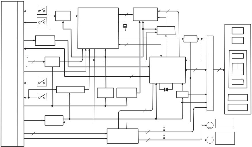
MP225,MP4026/G-KDC W4527/G/GY/Y,W427Y-KDC
DIAGRAM BLOCK
ELECTRIC UNIT (X25-)
TUNER
AM+B
SW5V
A8V
AUDIO OUT |
A8V |
|
|
|
BUFFER |
TUN SMETER
TUN SCL TUN SDA TUN IFC OUT
CD/VCD
CD SCL
CD SDA
CD MRST CD MSTOP CD MOTOR CD LOEJ CD LOS SW CD LOE LIM SW CD DISC12 SW CD DISC8 SW CD MUTE L CD MUTE R
VIDEO OUT
CH
LX RST
LX COM
LX CLK
LX DATA M
LX DATA S
LX REQ M
LX REQ S
LX MUTE
DXM-6540 |
: 810mV |
DXM-6560 |
: 1200mV |
DXM-6060 |
: 1200mV |
MECHA+B
A8V
BU5V
SERVO+B
to VIDEO OUT |
|
1Vpp@75 |
Term. |
|
|
1200mV |
|
BACK UP
3
ANALOG SW
IC7
RDS DECODER
A8V
SW5V
BUFFER
IC2 |
|
|
FM |
A8V |
|
|
||
AM |
|
|
MP |
E-VOL |
|
LEVEL |
||
& |
||
CD |
||
MPX |
||
|
||
CH |
|
|
AFS |
|
|
QUAL |
|
|
SW5V |
SW5V |
|
|
IC1 |
|
|
|
S-METER |
RDSDATA RDSCLK RDSQUAL |
AUXSW RDSAFS |
RDSNOISE |
AUD SCL |
|
|
|
AUD SDA |
|
|
|
|
|
SYSTEM |
|
|
|
MICROPROCESSOR |
|
EEPROM
MUTE PRE
MUTE
PWIC MUTE
PWIC BEEP
PWIC STBY
PARK SW
LINE MUTE
ACC DE
RST
IC6
MUTE |
|
DRIVER |
BU5V |
|
THERMAL |
|
PROTECT |
|
SW5V |
PRE MUTE
IC4
AUDIO
POWER
IC
|
|
AUX IN |
|
|
PRE OUT |
|
|
(REAR) |
MODE |
K-TYPE |
E-TYPE |
FM |
1800mV |
1372mV |
AM |
600mV |
855mV |
MP3 |
3600mV |
3600mV |
|
|
SP OUT |
PARK SW |
PARK SW |
TEL MUTE |
TEL MUTE |
ACC DET |
ACC |
SURGE DET |
BACK UP |
BU5V |
|
|
|
|
B.U DET |
|
|
|
|
|
|
|
TDFDET |
LDATAS LCLK LCE LDATAL LRST KEYREQ |
|
|
PON CD |
DSI |
REMO |
PON5 |
PS2-1 PS2-0 PS1-2 PS1-1 PS1-0 |
|
|
PANEL 5V |
|
|
|
BU5V |
|
|
|
|
SW5V |
|
|
|
IC2 |
|
|
IC1 |
REMOCON |
|
|
|
|
BU5V |
DSI |
LCD DRIVER |
RESET SW |
|
|
WITH |
|
|
|
KEY MATRIX |
|
|
|
LCD |
ILL SW |
|
|
|
|
|
|
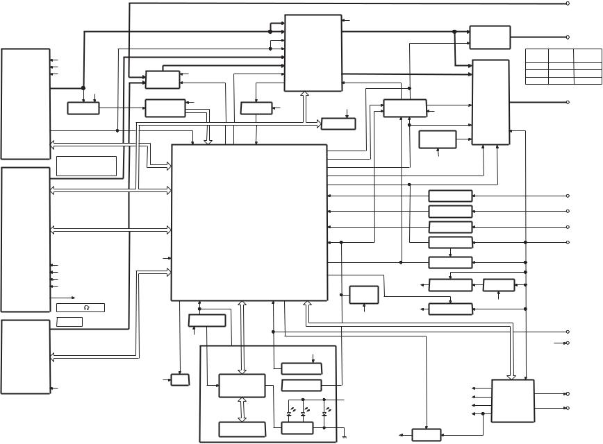
SWITCH UNIT (X16- ) |
|
|
|
B.U DET |
|
IC8 |
SERVO+B |
SERVO |
|
RESET |
|||
|
|
||
IC |
|
IC9 |
|
BU5V |
MECHA+B |
MECHA +B |
|
|
|
|
AM+B |
|
ILLUMI |
A8V |
|
ILLUMI |
||
|
||
|
BU5V |
|
SW5V |
SW 5V |
SW 14V |
|
SW5V |
|
|
WIRED REMO |
|
VIDEO OUT |
IC3 |
|
POWER |
ANT CON |
SUPPLY |
|
IC |
P CON |
MP225,MP4026/G-KDC W4527/G/GY/Y,W427Y-KDC DIAGRAM BLOCK
KDC-MP225,MP4026/G
KDC-W4527/G/GY/Y,W427Y
COMPONENTS DESCRIPTION
● SWITCH UNIT (X16-2640-xx/2642-xx/2652-xx)
Ref. No. |
Application / Function |
Operation / Condition / Compatibility |
|
|
|
IC1 |
LCD driver |
Drive for LCD unit |
|
|
|
IC2 |
Remote control IC |
Receiving for the remote control unit |
|
|
|
Q1 |
KEY scan detector |
key scan start at base gose “L”. |
|
|
|
Q2 |
key illumination SW |
Lights up for RED key illumination when base voltage level goes “H” |
|
|
|
Q3 |
key illumination SW |
Lights up for GREEN key illumination when base voltage level goes “H” |
|
|
|
● ELECTRIC UNIT (X25-9980-xx/9982-xx/X34-3172-70)
Ref. No. |
Application / Function |
|
|
|
Operation / Condition / Compatibility |
||
|
|
|
|
|
|
||
IC1 |
System microcomputer |
Control for TUNER unit, CD mechanism, volume & tone, LCD driver and external CD changer unit |
|||||
|
|
|
|
|
|
||
IC2 |
Electronic volume & N.C.MPX |
Control for source selector, volume & tone, and FM multiplex detector. |
|||||
|
|
|
|
|
|
||
|
|
Power supply for the units (Bu5V, Audio8V, FM+B, AM+B, P-con and ANT-con) |
|||||
|
|
|
|
|
|
|
|
|
|
|
SW1 |
|
OUT |
|
|
|
|
|
|
|
|
|
|
|
|
|
1.5~3.0V |
|
Audio ON |
|
|
|
|
|
|
|
|
|
|
|
|
|
3.5~5.0V |
|
Audio P-con ON |
|
|
IC3 |
Power supply IC |
|
|
|
|
|
|
|
7.0V~ |
|
Audio P-con, P-ant ON |
|
|||
|
|
|
|
|
|||
|
|
|
|
|
|
|
|
|
|
|
SW2 |
|
OUT |
|
|
|
|
|
|
|
|
|
|
|
|
|
2.0~3.0V |
|
Illumination, FM ON |
|
|
|
|
|
|
|
|
|
|
|
|
|
4.0V~ |
|
Illumination, AM ON |
|
|
|
|
|
|
|
|
||
|
|
|
|
|
|
|
|
IC4 |
Audio power amp IC |
Amplifier for audio signal to derive for 4channel speakers (50W maximum for each channel) |
|||||
|
|
|
|
|
|
||
IC6 |
Muting control IC |
Control for timing for mute |
|||||
|
|
|
|
|
|
|
|
IC7 |
RDS decoder |
Decode for RDS signal |
|
|
|||
|
|
|
|
|
|
||
IC8 |
Reset IC |
When detection voltage goes below 3.5V or less Reset IC output change to “L” signal |
|||||
|
|
|
|
|
|
||
IC9 |
Switching regulator |
Power supply for CD mecanism unit |
|||||
|
|
|
|
|
|
||
Q1 |
Serge detection |
When backup voltage become more than 24V output is “L” (momentary power down) / |
|||||
When backup voltage become less than 24V output is “H” |
|||||||
|
|
||||||
|
|
|
|
|
|
||
Q2 |
Backup detection |
When BU voltage supplied output is “L” / |
|||||
When BU voltage not supplied or momentary power down is detected output is “H” |
|||||||
|
|
||||||
|
|
|
|
|
|
||
Q3 |
ACC detection |
When ACC voltage supplied output is “L” |
|||||
|
|
|
|
|
|
||
Q4 |
SW 5V |
When base voltage is “L” Q4 is ON |
|||||
|
|
|
|
|
|
|
|
Q21,24 |
AVR |
Servo regulator |
|
|
|||
|
|
|
|
|
|
|
|
Q22 |
SW |
Servo SW |
|
|
|||
|
|
|
|
|
|
||
Q23 |
IC control |
Power supply IC controller |
|||||
|
|
|
|
|
|
||
Q41 |
SW |
Switching regulator control SW |
|||||
|
|
|
|
|
|
|
|
Q101 |
Buffer amp |
Composite signal buffer |
|
|
|||
|
|
|
|
|
|
||
Q151 |
DSI driver |
When base voltage level is “L” DSI LED is light up / When base voltage level is “H” DSI LED |
|||||
turns off / When panel assy is pull off, cut off the supply to panel 5V AVR. |
|||||||
|
|
||||||
|
|
|
|
|
|
|
|
Q201 |
Buffer amp |
Noise buffer amp |
|
|
|||
|
|
|
|
|
|
|
|
4
KDC-MP225,MP4026/G
KDC-W4527/G/GY/Y,W427Y
COMPONENTS DESCRIPTION
Ref. No. |
Application / Function |
Operation / Condition / Compatibility |
|
|
|
Q252 |
For surge measure of audio power IC |
When base voltage to “L”, for control to power IC function (STAND BY) |
|
|
|
Q350 |
Pre & NF mute SW |
When base voltage to “L”, drive to pre & NF mute SW (Q351) |
|
|
|
Q351 |
Pre mute SW |
When base voltage to “H”, muting to the pre Lch or NF Lch line |
|
|
|
Q352 |
Pre mute SW |
When base voltage to “H”, muting to the pre Rch or NF Rch line |
|
|
|
Q401 |
DSI illumination SW |
When base voltage to “H”, DSI illumination is light up. |
|
|
|
● CD PLAYER UNIT (X32-5500-00)
Ref. No. |
Application / Function |
Operation / Condition / Compatibility |
|
|
|
|
|
Generation of RF signal based on the signals from the APC circuit and pickup, and generation |
IC1 |
RF amplifier adapted for CD-RW |
of servo error (focusing error and tracking error) signals. Detection of dropout, anti-shock, |
|
|
track crossing and off-track conditions, included gain control function during CD-RW. |
|
|
|
|
|
Focusing, tracking, sled and spindle servo processing. Automatic adjustment (focusing, |
IC2 |
CD signal processor built-in MI-COM |
tracking, gain, offset and balance) operations. Digital signal processing (DSP, PLL, sub-codes, |
|
|
CIRC error correction, audio data Interpol ration) operations, and Microcomputer function. |
|
|
|
IC3 |
MP3/WMA decoder |
|
|
|
|
IC4 |
4CH BTL driver |
Focusing coil, tracking coil, spindle motor and sled motor driver, disc loading and eject operation. |
|
|
|
IC5 |
AVR |
For SW3.3V AVR |
|
|
|
IC6 |
AVR |
For BU3.3V AVR |
|
|
|
IC7 |
AVR |
For BU2.5V AVR |
|
|
|
IC8 |
Selector |
Serial audio signal selector IC |
|
|
|
IC9 |
AVR |
For IC2 (DAC section) 3.3V AVR |
|
|
|
Q1,3~7 |
Level shift |
3.3V → 5.0V |
|
|
|
Q8 |
APC |
LD power control |
|
|
|
Q9,10 |
SW |
Delay to sub beam line (antecedence beam) |
|
|
|
D2 |
Protection diode |
IC2 protection (for reset line) |
|
|
|
D3 |
Protection diode |
Laser diode protection |
|
|
|
5
KDC-MP225,MP4026/G KDC-W4527/G/GY/Y,W427Y
MICROCOMPUTER’S TERMINAL DESCRIPTION
● SYSTEM MICROPROCESSOR : 784225GC231A (X25 : IC1)
Pin No. |
Pin Name |
I/O |
|
|
Description / Processing Operation |
||
|
|
|
|
|
|
||
1 |
TUN SMETER |
I |
S meter detection input terminal |
|
|
||
|
|
|
|
|
|
||
2 |
RDS NOISE |
I |
FM noise detection input terminal |
|
|
||
|
|
|
|
||||
3 |
LINE MUTE |
I |
Phone Muting signal input terminal (More than 2.5V : NAVI mute, Less than 1.0V : TEL mute) |
||||
|
|
|
|
|
|
|
|
4 |
AVSS |
- |
GND |
|
|
|
|
|
|
|
|
|
|||
5 |
L RST |
O |
Reset signal output (for LCD driver) |
H : Light on display, key scan, L : Light out on display, key reset |
|||
|
|
|
|
|
|
|
|
6 |
L CE |
O |
CE output for LCD driver IC |
|
|
|
|
|
|
|
|
|
|
|
|
7 |
AVREF1 |
- |
BU5.0V |
|
|
|
|
|
|
|
|
|
|||
8 |
L DATAL |
I |
DATA input terminal from LCD derive IC |
|
|||
|
|
|
|
|
|||
9 |
L DATAS |
O |
DATA output terminal to LCD driver IC |
|
|||
|
|
|
|
|
|
||
10 |
L CLK |
O |
CLK output terminal to LCD driver IC |
|
|
||
|
|
|
|
|
|
||
11 |
TDF DET |
I |
Panel assy detect terminal |
|
H : Panel assy come off |
||
|
|
|
|
|
|
||
12 |
AUX ON |
O |
Select for AUX input signal |
|
H : AUX, L : Other |
||
|
|
|
|
|
|||
13 |
RDS QUAL |
I |
RDS decoder QUAL signal input terminal |
|
|||
|
|
|
|
|
|||
14 |
RDS DATA |
I |
RDS decoder Data signal input terminal |
|
|||
|
|
|
|
|
|
||
15 |
PWIC BEEP |
O |
Beep audio signal output terminal |
|
|
||
|
|
|
|
|
|
||
16 |
LX DATA S |
I |
DATA signal input from EXT. unit |
|
|
||
|
|
|
|
|
|
||
17 |
LX DATA M |
O |
DATA signal output to EXT. unit |
|
|
||
|
|
|
|
|
|
||
18 |
LX CLK |
I/O |
CLK signal input/output to EXT. unit |
|
|
||
|
|
|
|
|
|||
19 |
TUN SCL |
O |
I2C CLK signal output terminal (for front-end) |
|
|||
|
|
|
|
||||
20 |
TUN SDA |
I/O |
I2C DATA signal input/output terminal (for front-end) |
||||
|
|
|
|
|
|
||
21 |
TUN IFC OUT |
I |
IFC signal input terminal |
|
H : Station detect, L : No detect |
||
|
|
|
|
|
|||
22 |
RDS AFS |
O |
Time constant select terminal (for noise detect) |
H : Receiving, L : FM seek, AF search |
|||
|
|
|
|
||||
23 |
CD SDA |
I/O |
I2C DATA output terminal (for CD mechanism, electric VR) |
||||
|
|
|
|
||||
24 |
AUD SDA |
O |
CLK output terminal (for CD mechanism, electric VR) |
||||
|
|
|
|
|
|
|
|
25 |
NC |
- |
NC |
|
|
|
|
|
|
|
|
|
|
||
26 |
LX RST |
O |
Reset signal output to EXT. unit |
|
|
||
|
|
|
|
|
|||
27 |
LX CON |
O |
Control signal output to EXT. unit |
H: ON L: OFF |
|||
|
|
|
|
|
|||
28 |
LX MUTE |
I |
Request signal input terminal from EXT. unit |
L : Mute ON |
|||
|
|
|
|
|
|
||
29 |
LX REQ M |
O |
DATA signal output to EXT. unit |
|
|
||
|
|
|
|
|
|
||
30 |
PWIC SVR |
O |
SVR control for Audio power IC |
|
|
||
|
|
|
|
|
|||
31 |
PWIC STBY |
O |
STBY control for Audio power IC |
H : Power IC ON |
|||
|
|
|
|
|
|
||
32 |
PWIC MUTE |
O |
Muting control for Audio power IC |
|
|
||
|
|
|
|
|
|
|
|
33 |
VSS1 |
- |
GND |
|
|
|
|
|
|
|
|
|
|
||
34 |
ACC DET |
I |
ACC detection input terminal |
L : ACC detect |
|
||
|
|
|
|
|
|
|
|
35 |
RESET2 |
O |
Reset output terminal |
L : Active |
|
|
|
|
|
|
|
|
|
||
36 |
MUTE |
O |
Muting signal output terminal |
|
|
||
|
|
|
|
|
|
|
|
37 |
BU DET |
I |
BU detect input terminal |
|
L : BU detect |
|
|
|
|
|
|
|
|||
38 |
PARK SW |
I |
Packing condition detect terminal |
H : OFF, L : ON (PARKING) |
|||
|
|
|
|
|
|
||
39 |
PS2 1 |
O |
Power supply IC control terminal |
|
|
||
|
|
|
|
|
|
|
|
6
KDC-MP225,MP4026/G KDC-W4527/G/GY/Y,W427Y
MICROCOMPUTER’S TERMINAL DESCRIPTION
Pin No. |
Pin Name |
I/O |
Description / Processing Operation |
||
|
|
|
|
|
|
40 |
PS2 0 |
O |
Power supply IC control terminal |
|
|
|
|
|
|
|
|
41 |
PS1 0 |
O |
Power supply IC control terminal |
|
|
|
|
|
|
|
|
42 |
PS1 1 |
O |
Power supply IC control terminal |
|
|
|
|
|
|
|
|
43 |
PS1 2 |
O |
Power supply IC control terminal |
|
|
|
|
|
|
|
|
44 |
PON 5 |
O |
SW5V/SW14V control output terminal |
Hi-Z : OFF, L : ON |
|
|
|
|
|
|
|
45 |
NC |
- |
NC |
|
|
|
|
|
|
|
|
46 |
PON CD |
O |
MP3 power supply control terminal |
|
|
|
|
|
|
|
|
47 |
CD DISC12 SW |
I |
12cm CD disc eject SW detection input terminal |
L : 12cm disc |
|
|
|
|
|
|
|
48 |
CD MUTE R |
I |
Request for muting signal from CD mechanism |
L : Mute request |
|
|
|
|
|
|
|
49 |
NC |
- |
NC |
|
|
|
|
|
|
|
|
50 |
CE MRST |
O |
Reset signal output to CD mechanism |
L : Active |
|
|
|
|
|
||
51 |
CD DISC8 SW |
I |
8cm CD disc eject SW detection input terminal (Not used) |
||
|
|
|
|
|
|
52 |
CD LOS SW |
I |
Loading start SW detection input terminal |
L : Loading start |
|
|
|
|
|
|
|
53 |
CD MUTE L |
I |
Request for muting signal from CD mechanism |
L : Mute request |
|
|
|
|
|
|
|
54 |
NC |
- |
NC |
|
|
|
|
|
|
||
55 |
CD MSTOP |
O |
Request signal (Mechanism is STOP) output to CD mechanism L : Active |
||
|
|
|
|
|
|
56 |
CD LOE LIM SW |
I |
Down SW detection from CD mechanism |
|
|
|
|
|
|
|
|
57 |
CD LOEJ |
I/O |
CD mechanism loading / eject control terminal |
H : Eject, L : Loading |
|
|
|
|
|
|
|
58 |
CD MOTOR |
O |
CD mechanism motor loading control terminal |
H : Loading, Eject, Brake, L : Play |
|
|
|
|
|
|
|
59 |
DSI |
O |
Disc guide illumination control terminal |
H : DSI ON |
|
|
|
|
|
|
|
60 |
RESET |
I |
Reset input terminal L : Active |
|
|
|
|
|
|
|
|
61 |
NC |
- |
NC |
|
|
|
|
|
|
|
|
62 |
KEY REQ |
I |
Request for communication to slave unit |
L : Key input mode |
|
|
|
|
|
|
|
63 |
RDS CLK |
I |
RDS decoder CLK input terminal |
|
|
|
|
|
|
|
|
64 |
LX REQ S |
I |
DATA signal input from EXT. unit |
|
|
|
|
|
|
|
|
65 |
REMO |
I |
Remote control signal input terminal |
|
|
|
|
|
|
|
|
66 |
NC |
- |
NC |
|
|
|
|
|
|
|
|
67 |
VSS0 |
- |
GND |
|
|
|
|
|
|
|
|
68 |
VDD1 |
- |
BU5.0V |
|
|
|
|
|
|
|
|
69 |
X2 |
- |
Main clock input terminal (10MHz) |
|
|
|
|
|
|
|
|
70 |
X1 |
- |
Main clock input terminal (10MHz) |
|
|
|
|
|
|
|
|
71 |
TEST |
- |
GND |
|
|
|
|
|
|
|
|
72 |
XT2 |
- |
Sub clock input terminal (32.768kHz) |
|
|
|
|
|
|
|
|
73 |
XT1 |
- |
Sub clock input terminal (32.768kHz) |
|
|
|
|
|
|
|
|
74 |
VDD0 |
- |
BU5.0V |
|
|
|
|
|
|
|
|
75 |
AVDD |
- |
BU5.0V |
|
|
|
|
|
|
||
76~78 |
TYPE0~2 |
I |
Destination input terminal DXM6540 (SEL0 : Lo, SEL1 : Lo) |
||
|
|
|
|
|
|
79,80 |
TUN TYPE0,1 |
I |
Electric volume condition setting terminal |
|
|
|
|
|
|
|
|
7

KDC-MP225,MP4026/G KDC-W4527/G/GY/Y,W427Y
MICROCOMPUTER’S TERMINAL DESCRIPTION
● CD SIGNAL MICROPROCESSOR : UPD63712GC (X32 : IC2)
Pin No. |
Pin Name |
I/O |
|
|
Description / Processing Operation |
||||||
|
|
|
|
|
|
|
|
|
|
|
|
1 |
VREFL |
I |
Reference voltage input terminal |
|
|
||||||
|
|
|
|
|
|
|
|
|
|
|
|
2 |
AVSS |
- |
GND for ADC |
|
|
|
|||||
|
|
|
|
|
|
|
|
|
|
|
|
3 |
AVCC |
- |
Power supply for ADC (BU3.3V) |
|
|
||||||
|
|
|
|
|
|
|
|
|
|
|
|
4 |
NC |
O |
NC (OPEN) |
|
|
|
|||||
|
|
|
|
|
|
|
|
|
|||
|
|
|
|
|
|
|
|
|
|||
5 |
20RST |
O |
Reset control output terminal (for decoder) L : RESET, H : NORMAL |
||||||||
|
|
|
|
|
|
|
|
|
|||
6 |
20ACK |
I |
Acknowledge signal input terminal (for decoder) |
||||||||
|
|
|
|
|
|
|
|
|
|
||
7 |
20STBY |
O |
Standby control (for decoder) |
H : STAND BY, L : NORMAL |
|||||||
|
|
|
|
|
|
|
|
|
|
|
|
8,9 |
NC |
O |
NC (OPEN) |
|
|
|
|||||
|
|
|
|
|
|
|
|
|
|||
10 |
20INT |
I |
Interrupt signal input terminal (for decoder) |
||||||||
|
|
|
|
|
|
|
|
|
|
||
11 |
FOGUP |
I |
Interrupt for focus gain up control signal |
H : Focus gain UP, L : NORMAL |
|||||||
|
|
|
|
|
|
|
|
|
|
||
12 |
LZM |
I |
0 bit muting detect (Lch) |
L : MUTE OFF, H : MUTE ON |
|||||||
|
|
|
|
|
|
|
|
|
|
||
13 |
RZM |
I |
0 bit muting detect (Rch) |
L : MUTE OFF, H : MUTE ON |
|||||||
|
|
|
|
|
|
|
|
|
|
|
|
14,15 |
NC |
O |
NC |
|
|
|
|||||
|
|
|
|
|
|
|
|
|
|||
|
|
|
|
|
|
|
|
||||
16 |
20CS |
O |
Chip select signal output terminal (for decoder) |
||||||||
|
|
|
|
|
|
|
|
|
|||
|
|
|
|
|
|
|
|||||
17 |
20LP |
O |
Latch pules signal output terminal (for decoder) |
||||||||
|
|
|
|
|
|
|
|
|
|||
18 |
20TXD0 |
I/O |
Serial data signal output terminal (for decoder) |
||||||||
|
|
|
|
|
|
|
|
|
|||
19 |
20RXD0 |
I |
Serial data signal input terminal (for decoder) |
||||||||
|
|
|
|
|
|
|
|
|
|||
20 |
20SCLK0 |
O |
Serial data clock output terminal (for decoder) |
||||||||
|
|
|
|
|
|
|
|
|
|||
21 |
DSPTXD1 |
O |
Serial data signal output terminal (for DSP) |
||||||||
|
|
|
|
|
|
|
|
|
|||
22 |
DSPRXD1 |
I |
Serial data signal input terminal (for DSP) |
||||||||
|
|
|
|
|
|
|
|
|
|||
23 |
DSPSCLK1 |
O |
Serial data clock output terminal (for DSP) |
||||||||
|
|
|
|
|
|
|
|
|
|
||
24 |
AM0 |
I |
Select for ROM mode |
H : NORMAL, L : External ROM mode |
|||||||
|
|
|
|
|
|
|
|
|
|
|
|
25 |
DVCC |
- |
BU3.3V |
|
|
|
|||||
|
|
|
|
|
|
|
|
|
|
|
|
26 |
X2 |
O |
Oscillator (16MHz) |
|
|
|
|||||
|
|
|
|
|
|
|
|
|
|
|
|
27 |
DVSS |
- |
GND |
|
|
|
|||||
|
|
|
|
|
|
|
|
|
|
|
|
28 |
X1 |
I |
Oscillator (16MHz) |
|
|
|
|||||
|
|
|
|
|
|
|
|
|
|
|
|
29 |
AM1 |
I |
BU3.3V |
|
|
|
|||||
|
|
|
|
|
|
|
|
|
|||
|
|
|
|
|
|
||||||
30 |
RESET |
I |
Reset terminal L : RESET, H : NORMAL |
||||||||
|
|
|
|
|
|
|
|
|
|
|
|
31,32 |
NC |
O |
NC |
|
|
|
|||||
|
|
|
|
|
|
|
|
|
|
|
|
33,34 |
EMU0,1 |
O |
NC |
|
|
|
|||||
|
|
|
|
|
|
|
|
|
|
||
|
|
|
|
|
|
||||||
35 |
DSPSTB |
O |
Data strobe signal output terminal |
|
|||||||
|
|
|
|
|
|
|
|
|
|
||
36 |
DSPA0 |
O |
Command, parameter select signal |
H : Parameter, L : Command |
|||||||
|
|
|
|
|
|
|
|
|
|
||
|
|
|
|
|
|
||||||
37 |
DSPRST |
O |
Reset control output terminal (for DSP) |
|
|||||||
|
|
|
|
|
|
|
|
|
|
||
38 |
DSPINT |
I |
Interrupt signal input terminal (for DSP) |
H : Interrupt |
|||||||
|
|
|
|
|
|
|
|
|
|
||
39 |
/DAC RESET |
O |
Reset signal output terminal (for DSP) |
L : RESET, H : NORMAL |
|||||||
|
|
|
|
|
|
|
|
|
|
||
40 |
SEARCH |
O |
Search condition output terminal |
H : Search, L : NORMAL |
|||||||
|
|
|
|
|
|
|
|
|
|
||
41 |
LOE/LIM_SW |
I |
SLT SW detect input terminal |
H : Inside |
|||||||
|
|
|
|
|
|
|
|
|
|
|
|
42~45 |
NC |
O |
NC (OPEN) |
|
|
|
|||||
|
|
|
|
|
|
|
|
|
|
||
46 |
PONE5 |
O |
+5V AVR control terminal (for VIDEO) |
H : Power ON |
|||||||
|
|
|
|
|
|
|
|
|
|
||
47 |
PONE2.5 |
O |
+2.5V AVR control terminal (for VIDEO) |
H : Power ON |
|||||||
8
KDC-MP225,MP4026/G KDC-W4527/G/GY/Y,W427Y
MICROCOMPUTER’S TERMINAL DESCRIPTION
Pin No. |
|
|
|
Pin Name |
I/O |
|
|
Description / Processing Operation |
||||||
|
|
|
|
|
|
|
|
|
|
|
|
|
|
|
48,49 |
NC |
O |
NC (OPEN) |
|
|
|
|
|
||||||
|
|
|
|
|
|
|
|
|
|
|
||||
50 |
FLAGIN |
I |
C2 error detect terminal |
L : Correction OK, H : Correction NG |
||||||||||
|
|
|
|
|
|
|
|
|
|
|
|
|
|
|
51-60 |
NC |
O |
NC (OPEN) |
|
|
|
|
|
||||||
|
|
|
|
|
|
|
|
|
|
|
||||
61 |
/DAC PD |
O |
Reset control output terminal (for DAC) |
L : RESET, H : NORMAL |
||||||||||
|
|
|
|
|
|
|
|
|
|
|
|
|
|
|
62 |
DVSS |
- |
GND |
|
|
|
|
|
||||||
|
|
|
|
|
|
|
|
|
|
|||||
|
|
|
|
|
|
|
|
|
|
|||||
63 |
NMI |
I |
Request for non maskable interrupt signal input terminal |
|||||||||||
|
|
|
|
|
|
|
|
|
|
|
|
|
|
|
64 |
DVCC |
- |
+VCC |
|
|
|
|
|
||||||
|
|
|
|
|
|
|
|
|
|
|
|
|||
65 |
DAC MUTE |
O |
Muting control output terminal (for DAC) |
|
H : MUTE, L : MUTE OFF |
|||||||||
|
|
|
|
|
|
|
|
|
|
|
||||
66 |
DAC PON |
O |
Audio power supply (for DXM-6550) |
H : POWER ON |
||||||||||
|
|
|
|
|
|
|
|
|
|
|
|
|||
67 |
PONA5 |
O |
+5V Audio power supply (for DXM-6550) |
|
H : POWER ON |
|||||||||
|
|
|
|
|
|
|
|
|
|
|
|
|||
|
|
|
|
|
|
|
|
|
|
|||||
68 |
ESRST |
O |
Reset signal output terminal (for ES3890) |
|
L : RESET, H : NORMAL |
|||||||||
|
|
|
|
|
|
|
|
|
|
|
|
|||
69 |
VMUTE |
O |
Video mute control terminal |
|
H : MUTE ON, L : MUTE OFF |
|||||||||
|
|
|
|
|
|
|
|
|
|
|
|
|
|
|
70 |
NC |
O |
NC (OPEN) |
|
|
|
|
|
||||||
|
|
|
|
|
|
|
|
|
|
|
||||
71 |
SELINT |
O |
Video/Audio select output terminal |
H : NORMAL, L : Interrupt |
||||||||||
|
|
|
|
|
|
|
|
|
|
|
||||
72 |
ASEL0 |
O |
Audio signal output select control terminal 1 |
00 : STEREO, 01 : Lch |
||||||||||
|
|
|
|
|
|
|
|
|
|
|
||||
73 |
ASEL1 |
O |
Audio signal output select control terminal 1 |
10 : Rch, 11 : Not function |
||||||||||
|
|
|
|
|
|
|
|
|
|
|
|
|||
|
|
|
|
|
|
|
|
|
|
|||||
74 |
NT/PAL |
O |
NTSC/PAL select terminal |
|
L : NTSC, H : PAL |
|||||||||
|
|
|
|
|
|
|
|
|
|
|
|
|||
75 |
DATASEL |
O |
20F/ES3890 output select |
|
H : 20F, L : ES3890 |
|||||||||
|
|
|
|
|
|
|
|
|
|
|
|
|
|
|
76,77 |
NC |
O |
NC (OPEN) |
|
|
|
|
|
||||||
|
|
|
|
|
|
|
|
|
|
|
||||
78 |
NC (BOOT) |
I |
Flash memory writing terminal |
L : Writing, H : NORMAL |
||||||||||
|
|
|
|
|
|
|
|
|
|
|
|
|
|
|
79,80 |
NC |
O |
NC (OPEN) |
|
|
|
|
|
||||||
|
|
|
|
|
|
|
|
|
|
|
||||
81 |
POND3.3 |
O |
D3.3V power ON control terminal |
H : POWER ON |
||||||||||
|
|
|
|
|
|
|
|
|
|
|
|
|
||
|
|
|
|
|
|
|
|
|
|
|||||
82 |
MUTEL |
O |
Audio muting control terminal (Lch) |
|
|
|
||||||||
|
|
|
|
|
|
|
|
|
|
|
|
|
||
|
|
|
|
|
|
|
|
|
||||||
83 |
MUTER |
O |
Audio muting control terminal (Rch) |
|
|
|
||||||||
|
|
|
|
|
|
|
|
|
|
|
|
|
||
84 |
SDA |
I/O |
I2C data (for system microprocessor) |
|
|
|
||||||||
|
|
|
|
|
|
|
|
|
|
|
|
|||
85 |
SCL |
I/O |
I2C clock (for system microprocessor) |
|
|
|||||||||
|
|
|
|
|
|
|
|
|
|
|
||||
86 |
MSTOP |
I |
Interrupt signal for stand-by mode |
L : STOP, H : STOP cancellation |
||||||||||
|
|
|
|
|
|
|
|
|
|
|
|
|
|
|
87 |
NC |
O |
NC |
|
|
|
|
|
||||||
|
|
|
|
|
|
|
|
|
|
|||||
88 |
|
O |
Driver muting control L : MUTE ON, H : MUTE OFF |
|||||||||||
|
DMUTE |
|
||||||||||||
|
|
|
|
|
|
|
|
|
|
|
|
|
|
|
89 |
DVCC |
- |
+VCC |
|
|
|
|
|
||||||
|
|
|
|
|
|
|
|
|
|
|
|
|
|
|
90 |
NC |
O |
NC (OPEN) |
|
|
|
|
|
||||||
|
|
|
|
|
|
|
|
|
|
|
|
|
|
|
91 |
DVSS |
- |
GND |
|
|
|
|
|
||||||
|
|
|
|
|
|
|
|
|
|
|
|
|
|
|
92,93 |
NC |
I |
NC |
|
|
|
|
|
||||||
|
|
|
|
|
|
|
|
|
|
|
||||
94 |
MSEL |
I |
Memory capacity select input terminal |
H : Capacity Down, L : Capacity UP |
||||||||||
|
|
|
|
|
|
|
|
|
|
|
|
|
|
|
95 |
VCDSEL |
I |
NC |
|
|
|
|
|
||||||
|
|
|
|
|
|
|
|
|
|
|
||||
96 |
ASEL |
I |
Audio signal output polarity selector |
H : Reversal output, L : Noninversion output |
||||||||||
|
|
|
|
|
|
|
|
|
|
|
||||
97 |
CHSEL |
I |
Changer detect input terminal |
H : Changer, L : Normal |
||||||||||
|
|
|
|
|
|
|
|
|
|
|
||||
98 |
SEL0 |
I |
Destination input terminal |
DXM6540 (SEL0 : Lo, SEL1 : Lo) |
||||||||||
|
|
|
|
|
|
|
|
|
|
|
||||
99 |
SEL1 |
I |
Destination input terminal |
DXM6540 (SEL0 : Lo, SEL1 : Lo) |
||||||||||
|
|
|
|
|
|
|
|
|
|
|
|
|||
100 |
VREFH |
I |
ADC reference power supply (BU3.3V) |
|
|
|||||||||
|
|
|
|
|
|
|
|
|
|
|
|
|
|
|
9
KDC-MP225,MP4026/G KDC-W4527/G/GY/Y,W427Y
TEST MODE
1.How to enter test mode
While holding the FM key and PRESET 6 keys, reset the unit.
All display segments light up when the test mode is entered.
2.How to exit from test mode
Reset the unit.
Turning ACC off, power off, momentary power down or panel detaching does not terminate the test mode.
3.Initial status in the test mode
•Sources : ALL OFF (STAND BY)
•Display : All segments were lit.
•Volume : -10dB (displayed as “30”)
•Loudness : OFF
•CRSC : OFF regardless of the presence of switching function.
•Aux : ON
4. TUNER function
•Forced switching of K3I
Each press of the Preset 6 key in Tuner mode should switch K3I from AUTO→ Forced Wide→ Forced Middle→ Forced Narrow→ AUTO. The initial status is AUTO and the display
shows these modes as follows.
•AUTO : A
•Forced Wide : M
•Forced Middle : M
•Forced Narrow : N
•RDS check
PCON is power off when RDS data (“RDS test”) received for TUNER mode.
5. CD function
•Test mode specifications of the CD receiver
•Each press of the Track Up key jumps to the following track
numbers :
No. 9→ No. 15→ No. 10→ No. 11→ No. 12→ No. 13→ No. 22
→ No. 14→ No. 9 (The cycle restarts from here.)
•Each press of the Track Down key jumps to the previous track number to the track being played.
•When the number of total tracks of disc is nine or less, unit playback from a track 1.
•When the media to CD-DA, unit playback from track No. 28 by key operation of preset 1 key.
6. AUDIO function
•Audio-related specifications
•A short press of the Q key initiates the audio adjustment mode.
•Pressing the OPEN/CLOSE key on the remote controller initiates the audio adjustment mode.
•Continuous holding of a remote control key is inhibited.
•Bass, Middle and Treble are adjusted in 3 steps of -8 / 0 / +8 with the Track Up/down keys (default is 0).
•Balance is adjusted in 3 steps of Left L15 / 0 / R15 Max with the Track Up/down keys (default is 0).
•Loudness : OFF
7.MENU function
•Menu-related specifications
•A short press of the PLAY/PAUSE key initiates the Menu mode.
•Pressing the DNPP key on the remote initiates the Menu mode.
•Continuous holding of a remote control key is inhibited.
8.OTHER
•Special display when the display is all on
Pressing the Preset keys while the power is ALL OFF displays the following information.
[PRESET 1] |
Version display (Month/Day/Hour/Minute) |
|
|
[PRESET 2] |
ALL segment light up for FL display |
|
|
[PRESET 3] |
Short press : Display CD operation time. |
|
Long press/hold : Clear CD operation time |
|
|
[PRESET 5] |
Short press : Display CD ejection count. |
|
Long press/hold : Clear CD ejection count. |
|
|
[FM] |
ROM correction version. |
|
If not mounting ROM correction chip set display |
|
shows ROM No___ |
|
|
10
Loading...