


 Loading...
CD RECEIVER
KDC-1023/S KDC-122/S
SERVICE MANUAL
© 2002-11 PRINTED IN JAPAN B53-0005-00 (N) 1724
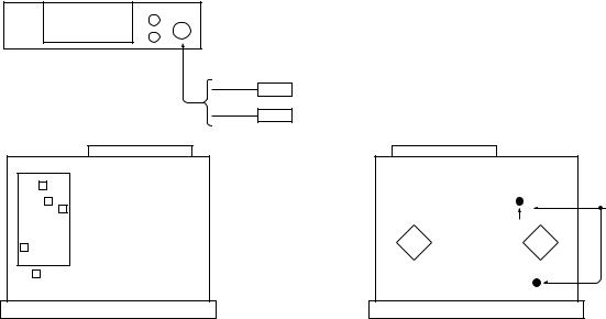
CD mechanism operation description is not in this sarvice manual. |
CD mechanism extension cord : W05-0618-00 |
|
Please, refer to sarvice manual X92-4030-0x (B51-7867-00). |
|
|
Panel assy |
Front glass |
Escutcheon |
(A64-2907-02): KDC-122 |
(B10-4355-01): KDC-122 |
(B07-3060-02): KDC-122 |
(A64-2908-02): KDC-122S |
(B10-4356-01): KDC-122S |
(B07-3022-02): KDC-122S |
KDC-122
COMPACT
DIGITAL AUDIO
45Wx4
 CRSC
CRSC
LOUD |
SCAN |
RDM |
REP |
CLK ADJ AUTO AME |
OFF |
|
|
|
AUD |
Panel assy |
Front glass |
Escutcheon |
(A64-2909-02): KDC-1023 |
(B10-4357-01): KDC-1023 |
(B07-3001-02): KDC-1023 |
(A64-2910-02): KDC-1023S |
(B10-4358-01): KDC-1023S |
(B07-3022-02): KDC-1023S |
KDC-1023
COMPACT
DIGITAL AUDIO
50Wx4
 CRSC
CRSC
LOUD |
SCAN |
RDM |
REP |
CLK ADJ AUTO AME |
OFF |
|
|
|
AUD |
DC cord |
Mounting hardware assy |
Lever |
Screw set |
(E30-4784-05) |
(J21-9716-03) |
(D10-4589-04)x2 |
(N99-1719-05) |

2
|
FM+B |
|
|
A8V |
|
|
|
FM(J,K) : 1800mV |
|
|
|
Q502 |
|
IC10 |
|
|
|
Q223,224 |
FM(E) : 1372mV |
CD : 3600mV |
|
|
|
|
|
|
|
|
PRE |
AM(J,K) : 600mV |
PRE |
|
ANT |
FM AGC |
|
FM AGC OUT |
|
|
AM(E) : 855mV |
CH : 3600mV |
|||
|
|
|
|
|
MUTE |
IC4 |
|
OUT |
||
|
AM+B |
|
|
|
|
|
|
|||
|
|
|
|
|
|
|
|
|
||
|
|
|
|
|
|
|
|
|
|
|
|
Q501 |
|
|
|
|
|
|
|
|
|
|
AM AGC |
|
AM AGC OUT |
|
|
IC8 |
POWER IC |
|
SP |
|
|
|
|
|
|
|
|
||||
|
|
|
|
TUNER,MPX & |
|
|
OUT |
|||
|
CD |
SERVO |
|
E-VOL. |
|
|
MUTE |
MUTE |
|
|
|
|
|
|
LOGIC |
|
|
||||
|
|
OUT |
|
|
|
|
|
|||
|
|
BU5V |
|
|
|
|
|
|
|
|
|
|
A8V |
|
TUNER |
|
|
|
|
|
|
|
AUDIO OUT |
1200mV |
CH |
|
|
|
Q10 |
|
|
|
|
|
|
|
|
|
|
||||
|
|
|
|
|
|
BU |
|
BACK |
||
|
|
|
CD |
|
|
|
|
|
||
|
12EJE |
|
|
|
|
|
DET |
|
UP |
|
|
|
|
|
|
|
|
|
|||
|
LO/S |
1200mV |
|
IC6 |
|
|
|
ACC |
|
|
|
SCLK |
|
|
IC12 |
|
|
||||
|
SDA |
|
|
|
|
|
EEP-ROM |
Q20 |
|
|
|
8EJE |
|
|
|
|
|
|
|
|
|
|
MUTE |
|
|
|
|
|
|
DET |
|
ACC |
|
RST |
|
|
RDS |
BU5V |
IC11 |
|
|
||
|
STOP |
|
|
|
|
|
||||
|
|
|
DECODER |
|
|
RESET |
|
IC7 |
|
|
|
LO/EJ |
|
|
|
|
|
|
|||
|
MO |
|
|
|
|
|
IC |
|
POWER |
|
|
LOE/LIM |
|
|
|
|
|
|
|
|
|
|
|
|
|
|
|
|
|
SUPPLY IC |
|
|
|
|
|
IC1 |
|
|
|
|
|
|
|
|
|
|
|
|
|
|
|
|
|
|
|
|
|
|
|
|
|
|
|
P-CON |
P-CON |
|
CHANGER |
|
|
|
|
|
|
|
P-ANT |
P-ANT |
|
|
|
|
|
|
|
|
|
|
|
|
AUDIO OUT |
|
|
|
|
|
|
Q51,55 |
|
|
|
RST |
|
|
MI-COM |
|
SERVO |
SERVO |
VCC |
|
|
|
REQ C |
|
|
|
|
|
|
|||
|
CLK |
|
|
|
|
|
|
|
SW1 |
|
|
DATA H |
|
|
|
|
|
|
|
SW2 |
|
|
CH-CON |
|
|
|
|
|
|
Q50 |
|
|
|
REQ H |
|
|
|
|
|
|
SW5V |
BU5V |
|
|
DATA C |
|
|
|
|
|
SW5V |
|
||
|
MUTE |
|
|
|
|
|
BU5V |
|
|
|
|
|
|
|
|
|
|
FM+B |
|
||
|
|
BACK UP |
|
|
|
|
FM+B |
|
||
|
|
|
|
|
|
AM+B |
AM+B |
|
||
|
|
|
|
|
|
|
|
|
||
|
|
|
|
BU5V |
|
|
SW5V |
A8V |
AUDIO+B |
|
|
|
|
|
|
|
|
ILLUMI |
|
||
|
|
|
|
|
|
IC2 |
BACKLIGHT |
|
||
|
|
|
|
|
|
|
|
|||
|
|
|
|
|
|
|
KEYILLUMI |
|
|
|
|
|
|
LCD |
LCD DRIVER |
|
|
REMOCON |
|
|
|
|
|
|
|
WITH |
|
|
|
|
|
|
|
|
|
|
KEY MATRIX |
|
|
|
|
|
|
1023/1023S/122/122S-KDC DIAGRAM BLOCK
KDC-1023/1023S/122/122S
COMPONENTS DESCRIPTION
● SWITCH UNIT (X16-1460-13/2370-11)
Ref.No. |
Application/Functions |
Operation/Condition/Compatibility |
IC1 |
LCD driver & key matrix |
|
|
|
|
Q1 |
Key scan start |
When Q1 base goes Lo, key scan start. |
|
|
|
● ELECTRIC UNIT (X25-9600-xx)
Ref.No. |
|
Application/Functions |
Operation/Condition/Compatibility |
IC1 |
System control µ-com |
System µ-com |
|
|
|
|
|
IC4 |
Power amplifire |
E-Vol output encoder power amplification for speaker. |
|
|
|
|
|
IC7 |
Power supply (Multi AVR) |
- |
|
|
|
|
|
|
|
|
When a pin 1, 2, or 13 is "H", MUTE turns on |
IC8 |
MUTE Logic |
When a pin 3, 4, or 5 is "H", P-AMP mute turns ON. |
|
|
|
|
Changer is RESET when a pin 9, 10, or 11 is "L". |
|
|
|
|
IC10 |
Tuner & E-Vol. |
FM/AM tuner & stereo decoder & E-Vol. |
|
|
|
|
|
IC11 |
Power on reset |
When B.U. 5V voltage is less than 3.5V, power reset. |
|
|
|
|
|
IC12 |
E2P-ROM |
Writing and read-out of adjustment data for a tuner |
|
|
|
|
|
Q10 |
B.U. detector |
BU on (base "H") : Collector "H" |
|
|
|
|
|
Q20 |
A.C.C |
detector |
ACC ON (base : "H") : Collector "L" |
|
|
|
|
Q40 |
MUTE |
driver |
Base "L" : Mute on (collector "L") |
|
|
|
|
Q50 |
SW 5V |
|
Base "L" : SW5V on |
|
|
|
|
Q51 |
SERBO AVR control |
Pin 2 "H" : Serbo on (pin 4 "H") |
|
|
|
|
|
Q53 |
|
|
|
|
|
|
|
Q55 |
SERBO AVR |
Base "H" : Serbo on |
|
|
|
|
|
Q70 |
Surge detector |
Base "H" : Surge detect |
|
|
|
|
|
Q223,224 |
MUTE |
|
Base "H" : Mute on |
|
|
|
|
Q251 |
|
|
|
|
|
|
|
Q501 |
AM RF amplifire |
Base "H" : Gain UP |
|
|
|
|
|
Q502 |
FM RF amplifire |
Gate "H" :Gain UP |
|
3
KDC-1023/1023S/122/122S
MICROCOMPUTER'S TERMINAL DESCRIPTION
● SYSTEM MICROCOMPUTER uPD780058GC501 (X25 : IC1)
|
Pin No. |
Name |
I/O |
Description |
|
Processing Operation |
||
|
|
|
|
|
|
|
||
|
1 |
TDF DET |
I |
Panel detection |
H:Panel detached |
L:Panel attached |
||
|
|
|
|
|
|
|||
|
2 |
8EJE SW |
I |
|
H:Eject is completed |
|||
|
|
Except 8cm CD model:always output L |
||||||
|
|
|
|
|
||||
|
3 |
NC |
O |
Not used (out put L) |
|
|
|
|
|
4 |
Avss |
|
|
|
|
|
|
|
|
|
|
|
H:Panel detached |
L:RESET |
||
|
5 |
L-RST |
O |
LCD driver RESET |
∆3 normal H , Power off L |
|||
|
|
|
|
|
When 7seg model,output L |
|||
|
|
|
|
|
|
|||
|
6 |
L-CE |
O |
LCD driver selection |
H:Select (panel communication) |
|||
|
When panel attached,output L |
|||||||
|
|
|
|
|
||||
|
7 |
AVREF1 |
|
|
|
|
|
|
|
8 |
NC |
|
Not used (connected to 9pin) |
|
|
|
|
|
9 |
IC10-DATA |
I/O |
IC10,E2PROM data communication |
∆3 non communication : H |
|||
|
10 |
IC10-CLK |
O |
IC10,E2PROM clock communication |
∆3 non communication : H |
|||
|
|
|
|
|
Non communication : H |
|||
|
11 |
L-DATAL |
I |
Data input from the LCD driver |
When panel detached : L |
|||
|
|
|
|
|
∆3 Pull down on X25 unit,Pull up on X16 unit |
|||
|
12 |
L-DATAS |
O |
Data output to the LCD driver |
When panel detached , output L |
|||
|
13 |
L-CLK |
O |
Clock output to the LCD driver |
When panel detached , output L |
|||
|
14 |
R-DATA |
I |
Data input from the RDS |
Except RDS model : output L |
|||
|
15 |
R-QUAL |
I |
Quality input from the RDS |
Except RDS model : output L |
|||
|
16 |
CH-DATAC |
I |
Data input from the changer (new 5L) |
Except changer model : output L |
|||
|
17 |
CH-DATAH |
O |
Data output to the changer (new 5L) |
When non communication ,last data keeping |
|||
|
Except changer model : output L |
|||||||
|
|
|
|
|
||||
|
|
|
|
|
|
|||
|
18 |
CH-CLK |
I/O |
Clock input/output with the Changer (new 5L) |
Check the old and new |
|||
|
Except changer model : output L |
|||||||
|
|
|
|
|
||||
|
|
|
|
|
|
|
|
|
|
19 |
CH-REQH |
O |
Request output to the changer (new 5L) |
L:Requset |
|
|
|
|
Except changer model : output L |
|||||||
|
|
|
|
|
||||
|
20 |
NC |
O |
Not used (output L) |
|
|
|
|
|
21 |
AFS |
O |
Noise detection time constant switching terminal |
H:Normal |
L:FM/AM seek and AF search |
||
|
∆3 (When tuner SRC auto zero , L) |
|||||||
|
22-24 |
NC |
O |
Not used (output L) |
|
|
|
|
|
25 |
CH-CONT |
O |
Changer control |
H:Changer on |
L:Changer off |
||
|
Except changer model : output L |
|||||||
|
|
|
|
|
||||
|
|
|
|
|
|
|||
|
26 |
TYPE REF |
O |
5V lines output for destination setting |
H:During destination reading |
|||
|
27 |
SD |
I |
Tuner SD input |
H:Station detected |
|
||
|
28 |
NC |
O |
Not used (output L) |
|
|
|
|
|
29 |
TYPE2 |
I |
Destination type selection terminal 2 |
Refer to destination type list. |
|||
|
30 |
TYPE1 |
I |
Destination type selection terminal 1 |
Refer to destination type list. |
|||
|
31 |
TYPE0 |
I |
Destination type selection terminal 0 |
Refer to destination type list. |
|||
|
32 |
TUNER-TYPE1 |
I |
Destination available/genuine model rool off |
H:genuine model 1 |
L:available model |
||
|
33 |
Vss1 |
|
|
|
|
|
|
|
34 |
TUNER-TYPE0 |
I |
Destination available/genuine model noise cancel |
H:genuine model 0 |
L:available model |
||
|
35 |
MUTE |
O |
Mute (E.Vol,Preset) control |
H:mute on |
L:mute off |
||
|
Power off after that 15 second L |
|||||||
|
|
|
|
|
||||
|
36 |
M-DATA |
I/O |
Data input/output with the CD mechanism |
∆3 non communication : H |
|||
|
37 |
M-CLK |
O |
Clock output to the CD mechanism |
∆3 non communication : H |
|||
|
|
|
|
|
When adjustment = H |
|||
|
38 |
ADJ |
O |
Tuner lines adjustment |
PS1-0,1=L |
|
PS1-2,2-0,1=Hi-z |
|
|
|
|
|
|
IC10-DATA,CLK=Hi-z |
|||
|
|
|
|
|
|
|
||
|
39 |
P-MUTE |
O |
Power IC mute control |
H:mute off |
L:mute on |
||
|
Power off after that 15 second H |
|||||||
|
|
|
|
|
||||
|
|
|
|
|
|
|||
|
40 |
SVR |
O |
Power IC servo control |
H:When momentary power down detected |
|||
|
L:Nomal |
|
|
|
||||
|
|
|
|
|
|
|
|
|
|
41 |
P-STBY |
O |
Power IC standby control |
H:Power IC ON |
L:Power IC OFF |
||
|
42 |
SW5V |
O |
SW 5V control |
H:SW5V OFF |
L:SW5V ON |
||
|
|
Power off after that 10 second H |
||||||
4 |
|
|
|
|
||||
|
|
|
|
|
|
|
|
|
|
|
|
|
|
|
|
|
|

KDC-1023/1023S/122/122S
MICROCOMPUTER'S TERMINAL DESCRIPTION
Pin No. |
Name |
I/O |
Description |
|
|
|
|
|
|
Processing Operation |
|
|
|
|
|
||||||||||||
|
|
|
|
|
|
|
|
|
|
|
|
|
|
|
|
|
|
|
|
|
|
||||||
43 |
B.U-DET |
I |
Back up detection terminal |
H:power down |
L:B.U. on |
|
|
|
|
|
|
|
|
||||||||||||||
44 |
ACC-DET |
I |
ACC detection terminal |
H:ACC OFF L:ACC ON |
|
|
|
|
|
|
|
|
|||||||||||||||
|
|
|
Power supply IC SW1 control 0 |
|
|
|
|
|
|
|
|
|
|
|
|
|
|
|
|
||||||||
45 |
PS1-0 |
O |
|
|
|
BA4911 SW1 |
|
|
Power supply IC output |
|
|||||||||||||||||
Audio 8V,P-CON |
|
PS1-2 |
|
PS1-1 |
|
PS1-0 |
|
A8V |
|
P-CON |
|
P-ANT |
|
||||||||||||||
|
|
|
|
|
|
|
|
|
|
||||||||||||||||||
|
|
|
|
|
|
L |
|
|
L |
|
|
L |
|
|
|
STANBY |
|
|
|
||||||||
|
|
|
Power supply IC SW1 control 1 |
|
|
|
|
|
|
|
|
|
|
||||||||||||||
46 |
PS1-1 |
O |
|
|
L |
|
L(H) |
|
H(L) |
|
ON |
|
OFF |
|
OFF |
|
|||||||||||
Audio 8V,P-CON |
|
|
|
|
|
|
|
|
|||||||||||||||||||
|
|
L |
|
|
H |
|
|
H |
|
ON |
|
ON |
|
|
OFF |
|
|||||||||||
|
|
|
|
|
|
|
|
|
|
|
|
|
|
||||||||||||||
47 |
PS1-2 |
O |
Power supply IC SW1 control 2 P-ANT |
|
|
H |
|
|
H |
|
|
H |
|
ON |
|
ON |
|
|
ON |
|
|||||||
|
|
|
|
|
|
|
|
|
|
|
|
|
|
|
|
|
|
|
|
|
|
|
|
|
|
|
|
48 |
PS2-0 |
O |
Power supply IC SW2 control 0 |
|
|
|
|
|
|
|
|
|
|
|
|
|
|
|
|
|
|
|
|
|
|
|
|
|
|
|
BA4911 SW2 |
|
Power supply IC output |
|
|
||||||||||||||||||||
ILL,FM,AM |
|
|
|
|
|
||||||||||||||||||||||
|
|
|
|
|
|
PS2-1 |
|
PS2-0 |
|
ILLUMI |
|
FM |
|
AM |
|
|
|||||||||||
|
|
|
|
|
|
|
|
L |
|
L |
|
|
|
|
|
STANBY |
|
|
|
|
|
||||||
|
|
|
|
|
|
|
|
|
|
|
|
|
|
|
|
|
|||||||||||
49 |
PS2-1 |
O |
Power supply IC SW2 control 1 |
|
|
|
L(H) |
|
H(L) |
|
ON |
|
|
ON |
|
OFF |
|
|
|||||||||
|
|
|
|
H |
|
H |
|
|
ON |
|
|
OFF |
|
ON |
|
|
|||||||||||
ILL,FM,AM |
|
|
|
|
|
|
|
|
|
|
|
||||||||||||||||
|
|
|
|
|
|
|
|
|
|
|
|
|
|
|
|
|
|
|
|
|
|
|
|
|
|
||
|
|
|
|
|
|
|
|
|
|
|
|
|
|
|
|
|
|
|
|
|
|
|
|
|
|
|
|
50 |
BEEP |
|
BEEP |
|
|
|
|
|
|
|
|
|
|
|
|
|
|
|
|
|
|
|
|
|
|
|
|
|
|
|
|
H:Light on |
|
L:Light off |
|
|
|
|
|
|
|
|
|
|
|||||||||||
51 |
DSI |
O |
DSI control |
When panel attached,output L |
|
|
|
|
|
||||||||||||||||||
When panel detached,flashing at the panel (H/L) |
|||||||||||||||||||||||||||
|
|
|
|
||||||||||||||||||||||||
|
|
|
|
FIX model is output L |
|
|
|
|
|
|
|
|
|
|
|||||||||||||
52 |
NC |
O |
Not used (out put L) |
|
|
|
|
|
|
|
|
|
|
|
|
|
|
|
|
|
|
|
|
|
|
|
|
53 |
NC |
O |
Not used (out put L) |
|
|
|
|
|
|
|
|
|
|
|
|
|
|
|
|
|
|
|
|
|
|
|
|
54 |
LOE/LIM SW |
I |
CD mechanism down&limit detection |
H:Chucking detection L:Normal |
|
|
|
|
|
||||||||||||||||||
55 |
MO SW |
O |
CD mechanism loading motor control output |
H:Loading,Eject,Break |
L:Play |
|
|
|
|
|
|||||||||||||||||
56 |
LO/EJ |
I/O |
CD mechanism loading/Eject switching terminal |
H:Eject |
|
L:Loading |
|
|
|
|
|
|
|
|
|
|
|||||||||||
57 |
M-STOP |
O |
Stop output to the CD mechanism |
H:Play |
|
L:Stop |
|
|
|
|
|
|
|
|
|
|
|
|
|
|
|||||||
58 |
M-RST |
O |
Reset output to the CD mechanism |
H:Normal |
L:CD mechanism reset |
|
|
|
|
|
|||||||||||||||||
59 |
M-MUTE |
I |
Mute input from the CD mechanism |
H:mute off |
|
L:mute on |
|
|
|
|
|
|
|
|
|
|
|||||||||||
60 |
RESET |
|
Reset input from the System microcomputer |
|
|
|
|
|
|
|
|
|
|
|
|
|
|
|
|
|
|
|
|
|
|
|
|
61 |
REMO |
I |
Remote control input |
|
|
|
|
|
|
|
|
|
|
|
|
|
|
|
|
|
|
|
|
|
|
|
|
62 |
R-CLK |
I |
RDS clock input |
Except RDS model : output L |
|
|
|
|
|
||||||||||||||||||
|
|
|
|
H:Changer detection |
|
|
|
|
|
|
|
|
|
|
|||||||||||||
63 |
CH-REQC |
I |
Request input from the changer (new 5L) |
L:Request |
|
|
|
|
|
|
|
|
|
|
|
|
|
|
|
|
|
||||||
|
|
|
|
Except Changer model : output L |
|
|
|
|
|
||||||||||||||||||
|
|
|
|
|
|
|
|
|
|
|
|
|
|
|
|
|
|
|
|
|
|
|
|
|
|||
64 |
LOS SW |
I |
CD mechanism loading's switch detected |
H:No disc |
|
|
|
|
|
|
|
|
|
|
|
|
|
|
|
|
|
||||||
L:DISK IN(Loading Start) |
|
|
|
|
|
|
|
|
|||||||||||||||||||
|
|
|
|
|
|
|
|
|
|
|
|
||||||||||||||||
|
|
|
|
|
|
|
|
|
|
|
|
|
|
|
|
|
|
|
|
|
|
|
|
||||
65 |
KEY-REQ |
I |
Key input detected |
H:Key no input |
|
|
|
|
|
|
|
|
|
|
|
|
|
|
|||||||||
(11pin L connected to the DATA L) |
L:Key input (edge key data reading start) |
||||||||||||||||||||||||||
|
|
|
|||||||||||||||||||||||||
66 |
12EJE SW |
I |
12cm disc detected |
L:12cm disc |
|
|
|
|
|
|
|
|
|
|
|
|
|
|
|||||||||
67 |
Vss0 |
|
|
|
|
|
|
|
|
|
|
|
|
|
|
|
|
|
|
|
|
|
|
|
|
|
|
68 |
VDD1 |
|
|
|
|
|
|
|
|
|
|
|
|
|
|
|
|
|
|
|
|
|
|
|
|
|
|
69 |
X2 |
|
∆3 MAIN X'tal oscillating circuit |
∆3 |
|
4.19MHz X'tal connection |
|
|
|
|
|
||||||||||||||||
70 |
X1 |
|
∆3 MAIN X'tal oscillating circuit |
∆3 |
|
4.19MHz X'tal connection |
|
|
|
|
|
||||||||||||||||
71 |
IC |
|
TEST |
|
|
|
|
|
|
|
|
|
|
|
|
|
|
|
|
|
|
|
|
|
|
|
|
72 |
XT2 |
|
Not used |
OPEN |
|
|
|
|
|
|
|
|
|
|
|
|
|
|
|
|
|
|
|
||||
73 |
XT1 |
|
|
|
|
|
|
|
|
|
|
|
|
|
|
|
|
|
|
|
|
|
|
|
|
|
|
74 |
VDD0 |
|
VDD |
Connected to VDD |
|
|
|
|
|
|
|
|
|
|
|||||||||||||
75 |
AVREF0 |
|
A/D converter reference voltage control output, |
|
|
|
|
|
|
|
|
|
|
|
|
|
|
|
|
|
|
|
|
|
|
|
|
|
connection to the 80pin AVCONT |
|
|
|
|
|
|
|
|
|
|
|
|
|
|
|
|
|
|
|
|
|
|
|
|||
|
|
|
|
|
|
|
|
|
|
|
|
|
|
|
|
|
|
|
|
|
|
|
|
|
|
||
76 |
S-METER |
I |
S-meter input |
|
|
|
|
|
|
|
|
|
|
|
|
|
|
|
|
|
|
|
|
|
|
|
|
77 |
NOISE |
I |
FM noise detection input |
∆3 |
|
|
|
|
|
|
|
|
|
|
|
|
|
|
|
|
|
|
|
|
|
||
|
|
|
|
2.5V or greater:NAVI MUTE |
|
|
|
|
|
||||||||||||||||||
78 |
PHONE |
I |
2way mute |
1.0V or less:TEL MUTE |
|
|
|
|
|
|
|
|
|
|
|||||||||||||
|
|
|
|
Except phone mute model : output L |
|
|
|
||||||||||||||||||||
79 |
NC |
O |
Not used (out put L) |
|
|
|
|
|
|
|
|
|
|
|
|
|
|
|
|
|
|
|
|
|
|
|
|
80 |
AVCONT |
O |
A/D converter standard voltage control output |
H:During A/D converter active |
|
|
|
|
|
||||||||||||||||||
same timing with PON |
|
|
|
|
|
|
|
|
|
|
|||||||||||||||||
|
|
|
|
|
|
|
|
|
|
|
|
|
|
||||||||||||||
5
KDC-1023/1023S/122/122S
MICROCOMPUTER'S TERMINAL DESCRIPTION
● MECHANISM MICROCOMPUTER MN6627771KP (X32 : IC2)
|
Pin No. |
Name |
I/O |
Description |
Processing Operation |
|
|
|
|
|
|
|
1 |
TVD |
O |
Traverse driver output (PWM output) |
|
|
|
|
|
|
|
|
2 |
SPL |
O |
Spindle motor drive output (PWM output) |
|
|
|
|
|
|
|
|
3 |
PC |
O |
Spindle motor ON output |
L:ON H:OFF (default ) |
|
|
|
|
|
|
|
4 |
PWM |
O |
multi-purpose PWM output |
It's possible to setup the TOSF2 |
|
|
|
|
|
|
|
5 |
TBAL |
O |
Tracking balance adjust output (PWM output) |
|
|
|
|
|
|
|
|
6 |
FBAL |
O |
Focus balance adjust output (PWM output) |
|
|
|
|
|
|
|
|
7 |
NRFDET |
I |
RF detection signal input |
L:detected |
|
|
|
|
|
|
|
8 |
OFT |
I |
Off-track signal input |
H:detected |
|
|
|
|
|
|
|
9 |
BDO |
I |
Drop out signal input |
H:detected |
|
|
|
|
|
|
|
10 |
LDON |
O |
Laser on signal output H:ON |
When command FO on,LDON is H |
|
|
|
|
|
|
|
11 |
DSLB |
O |
DSL balance output |
|
|
|
|
|
|
|
|
12 |
DVDD1 |
- |
Power supply for digital circuit |
|
|
|
|
|
|
|
|
13 |
DVSS1 |
- |
Ground lines for digital circuit |
|
|
|
|
|
|
|
|
14 |
AVSS2 |
- |
Ground lines for analog circuit |
For DSL,PLL and AD |
|
|
|
|
|
|
|
15 |
DSLF |
I/O |
Loop filter terminal for DSL |
The bias of ARF output terminal in one |
|
|
|
|
|
|
|
16 |
ARF |
I |
RF signal input |
|
|
|
|
|
|
|
|
17 |
RFSW |
I |
When DSL circuit,constant switch terminal |
|
|
|
|
|
|
|
|
18 |
PLLF |
I/O |
Loop filter terminal for PLL |
|
|
|
|
|
|
|
|
19 |
PLLF2 |
I/O |
Loop filter characteristic switching terminal for PLL |
|
|
|
|
|
|
|
|
20 |
IREF |
I |
Standard voltage input terminal |
|
|
|
|
|
|
|
|
21 |
RFENV |
I |
RF envelope signal input |
Analog input |
|
|
|
|
|
|
|
22 |
TRCRS |
I |
Track cross signal input |
Analog input |
|
|
|
|
|
|
|
23 |
TE |
I |
Tracking error signal input |
Analog input |
|
|
|
|
|
|
|
24 |
FE |
I |
Focusing error signal input |
Analog input |
|
|
|
|
|
|
|
25 |
AVDD2 |
- |
Power supply for analog circuit |
For DSL,PLL and AD |
|
|
|
|
|
|
|
26 |
AVSS1 |
- |
Ground lines for analog circuit |
For audio output (Lch and Rch in one) |
|
|
|
|
|
|
|
27 |
OUTR |
O |
Rch audio output |
|
|
|
|
|
|
|
|
28 |
AVDD1 |
- |
Power supply for analog circuit |
For audio output (Lch and Rch in one) |
|
|
|
|
|
|
|
29 |
OUTL |
O |
Lch audio output |
|
|
|
|
|
|
|
|
30 |
DVSS3 |
- |
Ground lines for digital circuit |
|
|
|
|
|
|
|
|
31 |
CSEL |
I |
Oscillation frequency specification terminal |
H:33.8488MHz L:16.9344MHz |
|
|
|
|
|
|
|
32 |
NC |
O |
Not used |
|
|
|
|
|
|
|
|
33 |
ASEL |
I |
Audio output polarity switching terminal |
L:Reverse H:Non reverse |
|
|
|
|
|
|
|
34 |
MSEL0 |
I |
Destination type selection port (set 2bit) |
Order "MSEL 0" and "MSEL 1" Set up |
|
|
|
|
|
|
|
35 |
MSEL1 |
I |
Destination type selection port (set 2bit) |
Order "MSEL 0" and "MSEL 1" Set up |
|
|
|
|
|
|
|
36 |
ICRST |
O |
Reset control terminal for external DAC |
|
|
|
|
|
|
|
|
37 |
BCLK |
O |
Bit clock output for serial data |
|
|
|
|
|
|
|
|
38 |
LRCK |
O |
L/R identification signal output |
|
|
|
|
|
|
|
|
39 |
SRDATA |
O |
Sirial data output |
|
|
|
|
|
|
|
|
40 |
VREFP |
I |
A/D converter standard power supply input |
|
|
|
|
|
|
|
|
41 |
HOT |
I |
Temperature protection detection terminal (AD input) |
Over C5(h):on |
|
|
|
|
|
|
|
42 |
8EJE_SW |
I |
8cm disc eject stop detection terminal |
H:Stop |
|
|
|
|
|
|
|
43 |
12EJE/SDET_SW |
I |
Judge the 8cm or 12cm disc |
12cm disc stop detection terminal |
|
|
|
|
|
|
|
44 |
LOE/LIM_SW |
I |
Pick-up inside detected |
Loading end detection terminal |
|
|
|
|
|
|
|
45 |
PCK |
O |
PLL extracted clock output,etc |
|
|
|
|
|
|
|
|
46 |
EFM |
O |
EFM signal output,etc |
|
|
|
|
|
|
|
|
47 |
SENSE |
O |
Optics servo status signal output,etc |
|
|
|
|
|
|
|
|
48 |
CLVS |
O |
Spindle servo phase synchronous signal output,etc |
L:Normal operation H:Luff servo |
|
|
|
|
|
|
|
49 |
DEMPH |
O |
Dephase detection signal output,etc |
H:on |
|
|
|
|
|
|
|
50 |
DVDD2 |
- |
Power supply for digital circuit |
|
|
|
|
|
|
|
6 |
51 |
X1 |
I |
Main clock input terminal |
|
|
|
|
|
|

KDC-1023/1023S/122/122S
MICROCOMPUTER'S TERMINAL DESCRIPTION
Pin No. |
Name |
I/O |
Description |
Processing Operation |
|
|
|
|
|
52 |
X2 |
O |
Main clock output terminal |
|
|
|
|
|
|
53 |
DVSS2 |
- |
Ground lines for digital circuit |
|
|
|
|
|
|
54 |
XSUB1 |
I |
When external DAC,external clock input terminal |
|
|
|
|
|
|
55 |
XSUB2 |
O |
|
|
|
|
|
|
|
56 |
TEST1 |
I |
Test port 1 |
Normal operation is H fixed |
|
|
|
|
|
57 |
TEST2 |
I |
Test port 2 |
Normal operation is H fixed |
|
|
|
|
|
58 |
NC |
O |
Not used |
|
|
|
|
|
|
59 |
VER/HOR |
O |
Put length or breadth switching motor terminal |
H:Put length L:Put breadth |
|
|
|
|
|
60 |
DRV_MUTE |
O |
Driver mute control terminal |
L:MUTE ON H:MUTE OFF |
|
|
|
|
|
61 |
/MUTE_L |
O |
Audio Lch MUTE output |
L:MUTE |
|
|
|
|
|
62 |
/MUTE_R |
O |
Audio Rch MUTE output |
L:MUTE |
|
|
|
|
|
63 |
/RST |
I |
LSI reset input terminal |
H:Normal L:Reset |
|
|
|
|
|
64 |
OCD_CLK |
I |
When OCD connected, clock input |
|
|
|
|
|
|
65 |
/MSTOP |
I |
Standby detection terminal |
H:Normal L:Mecha stop |
|
|
|
|
|
66 |
DATA |
I/O |
I2C bus data line (communication line with system computer) |
At that time serial writer connected |
|
|
|
|
|
67 |
SBIO |
I |
When connected to serial writer,data input terminal |
|
|
|
|
|
|
68 |
/CLK |
I/O |
I2C bus clock line (communication line with system computer) |
At that time serial writer connected |
|
|
|
|
|
69 |
TX |
O |
Digital audio interface signal output |
|
|
|
|
|
|
70 |
EQCNT |
O |
RF EQ switching terminal |
L:x2 times H:x1 times |
|
|
|
|
|
71 |
XSEL |
I |
During the external DAC connection |
MCLK external input (H:input) |
|
|
|
|
|
72 |
MCNT |
I |
CD mecha Loading/Eject control ON/OFF |
L:OFF (HOST control) H:mechanism control |
|
|
|
|
|
73 |
P-ON |
O |
Audio and servo origin power control terminal |
L:power on H:power off |
|
|
|
|
|
74 |
MOTOR |
O |
Loading/Eject control switching terminal |
At that time LO/EJ is "H" |
|
|
|
|
|
75 |
LO/EJ |
O |
Loading/Eject control terminal or output L |
When 72pin (P82) is "L",output "L" |
|
|
|
|
|
76 |
CD-RW |
O |
CD-RW control terminal |
H:CD-RW L:normal |
|
|
|
|
|
77 |
LDCNT |
O |
LD control terminal |
Operation is same LDON as timing |
|
|
|
|
|
78 |
DVDD3 |
- |
Power supply for digital circuit |
|
|
|
|
|
|
79 |
FOD |
O |
Focus driver output (PWM output) |
|
|
|
|
|
|
80 |
TRD |
O |
Tracking driver output (PWM output) |
|
System mi-com Destination type list
|
TYPE2 |
TYPE1 |
TYPE0 |
MODEL NAME |
|
|
|
|
|
|
|
|
L |
L |
L |
KDC-2024SA/SYA, 2024SG/SYG |
|
|
|
|
|
|
|
uPD780058GC499 |
L |
L |
H |
KDC-2022, 2022V,202MR |
|
|
|
|
|
||
L |
H |
L |
RY-391CD, RX-491CD |
||
|
|||||
|
|
|
|
|
|
|
L |
H |
H |
KDC-4023, 2023, 3023 |
|
|
|
|
|
|
|
|
L |
L |
H |
KDC-122, 122S |
|
|
|
|
|
|
|
uPD780058GC501 |
L |
H |
H |
KDC-1023, 1023S |
|
|
|
|
|
|
|
|
H |
L |
H |
KDC-222, 222S |
|
|
|
|
|
|
|
|
L |
L |
L |
KDC-3024G/YG, 307G/YG |
|
|
|
|
|
|
|
uPD780058GC502 |
L |
H |
H |
KDC-3023R |
|
|
|
|
|
||
H |
L |
L |
KDC-3024A/YA, 307A/YA |
||
|
|||||
|
|
|
|
|
|
|
H |
L |
H |
KDC-4024/Y/V/YV |
|
|
|
|
|
|
|
uPD780058GC503 |
L |
L |
L |
KDC-2094YA/YG |
|
|
|
|
|
|
|
H: |
R135 |
R137 |
R139 |
|
|
|
|
|
|
|
|
L: |
R136 |
R138 |
R140 |
|
|
|
|
|
|
|
7
KDC-1023/1023S/122/122S
ADJUSTMENT
1.IC10 (TDA7513) -The Tuner adjustment method
•When IC10 and its circumference are fixed, according to the following order, it readjusts if needed.
•The adjustment item changes with parts to exchange. Please refer to "Parts vs Adjustment item table".
1-1. VCO Coil Adjustment -- Adjustment of Tunning Voltage
Voltage Check Point |
|
: Vt-Check Land |
|
|||
|
|
|
|
(PWB Side_B, around D506) |
||
Adjustment Coil |
|
: L507 (VCO Coil) |
|
|||
The adjustment method |
: VCO coil is turned and adjusted |
|||||
|
|
|
|
according to the following tables. |
||
|
|
|
|
|
|
|
TYPE |
Mode |
|
|
freq. |
Voltage |
Fig |
|
|
|
|
|
|
|
E/M |
AM |
|
1611kHz |
5.5 ± 0.1(V) |
(C) |
|
|
|
|
|
|
|
|
K |
AM |
|
1700kHz |
5.8 ± 0.1(V) |
(C) |
|
|
|
|
|
|
|
|
J |
FM |
|
90.0MHz |
5.6 ± 0.1(V) |
(C) |
|
|
|
|
|
|
|
|
W(Wide Band) |
FM |
|
108.0MHz |
7.2 ± 0.1(V) |
(C) |
|
M : AM Adjustment
For Your Information : The frequency of SET is only set up by Pre-Set-Key in case this adjustment
1-2. Adjustment of 1st & 2nd-MIX Coil |
|
|
||||
Voltage Check Point |
: S_METER-Check Land |
|
||||
|
|
|
(PWB Side_B, around W572) |
|||
Adjustment Coil |
|
: 1stIFT = L508 / 2ndIFT = L509 |
||||
Setting of Signal Generator : Refer to the following tables |
||||||
|
|
|
|
|
|
|
TYPE |
MODE |
freq. |
Mod. |
|
ANT Input |
Fig |
|
|
|
|
|
|
|
K |
AM |
1000kHz |
OFF |
|
35dBuEMF |
(B),(C) |
|
|
|
|
|
|
|
E,M,J,W |
AM |
999kHz |
OFF |
|
35dBuEMF |
(B),(C) |
|
|
|
|
|
|
|
The appearance and the coil with which S-METER DC voltage serves as the maximum are turned and adjusted
in the above-mentioned SG input.
By the above-mentioned adjustment method, same adjustment is performed to both sides (1st&2nd MIX Coil).
(REAR VIEW) |
|
|
|
(TUNER ANT) |
|
[Fig.1] |
FM-SG |
(A) |
|
AM-SG |
(B) |
L505
L506
L507
L508
L509
(OVER VIEW)
[Fig.2]
1-3. Adjustment of FM_ANT&RF Coil |
|
|
||||||
Voltage Check Point |
: S_METER-Check Land (PWB |
|||||||
|
|
|
|
|
Side_B, around W572) |
|
||
Adjustment Coil |
|
: ANT_Coil = L505 |
|
|||||
|
|
|
|
|
RF_Coil = L506 |
|
||
Setting of Signal Generator : Refer to the following tables. |
||||||||
|
|
|
|
|
|
|
|
|
TYPE |
MODE |
|
freq. |
|
Mod. |
|
ANT Input |
Fig |
|
|
|
|
|
|
|
|
|
E/M |
FM |
|
87.5MHz |
|
OFF |
|
5 or 11dBuEMF |
(A),(C) |
|
|
|
|
|
|
|
|
|
K |
FM |
|
87.9MHz |
|
OFF |
|
5 or 11dBuEMF |
(A),(C) |
|
|
|
|
|
|
|
|
|
J |
FM |
|
76.0MHz |
|
OFF |
|
5 or 11dBuEMF |
(A),(C) |
|
|
|
|
|
|
|
|
|
W(Wide Band) |
FM |
|
65.0MHz |
|
OFF |
|
5 or 11dBuEMF |
(A),(C) |
|
|
|
|
|
|
|
|
|
The appearance and the coil with which S-METER DC voltage serves as the maximum are turned and adjusted
in the above-mentioned SG input.
By the above-mentioned adjustment method, same adjustment is performed to both sides (ANT&RF Coil).
1-4. Adjustment of STEREO (adjustment of 456k-VCO)
Adjust in TEST_MODE
•How to enter the test mode
While pressing on [ FM ] and [ PRESET 6 ] keys, reset the unit.
•Adjustment method
Complete on condition that show "ALL OFF" when pressing on [ PRESET 1 ] and [ PRESET 6 ] keys.
(Writing adjustment valve to the EEPROM.)
Effect of adjustment is in cofirmation of adjustment status at [ PRESET 4 ] key.
•Display of [ PRESET 4 ]
Adjustment "OK" : 14seg model "E2P OK" 7seg model "EPO" Adjustment "NG" : 14seg model "E2P ERR" 7seg model "EPE"
•Releasing the test mode Reset mode only.
ACC off, Power off, Power down and Remove the panel mode is not releasing.
(C) DC Voltmeter
Vt
Check Land
IC10
S-METER
Check Land
(UNDER VIEW)
[Fig.3]
8
KDC-1023/1023S/122/122S
ADJUSTMENT
2.IC10 (TDA7513) Replacement-Parts vs Adjustment Item Table
•When the parts in the following tables are exchanged, please readjust according to a table.
•When other parts are exchanged, please perform only a check of operation. There is no necessity for readjustment.
Replacement parts |
|
|
|
Adjustment Item |
|
|
|||
|
|
|
|
|
|
|
|
|
|
|
|
|
|
|
|
|
|
|
|
Parts Name |
Ref |
TYPE |
Parts Number |
VCOVt |
1st MIX |
2nd MIX |
ANT |
RF Coil |
Stereo |
Number |
Coil |
||||||||
|
IC10 |
ALL |
TDA7513 |
™ |
™ |
™ |
™ |
™ |
™ |
|
|
|
|
|
|
|
|
|
|
EEP-ROM |
|
|
M24C01-WMN6T |
|
|
|
|
|
|
|
IC12 |
ALL |
BR24C01AF-W |
™ |
™ |
™ |
™ |
™ |
™ |
|
|
|
S-24CS02AFJ-TB |
|
|
|
|
|
|
|
|
|
|
|
|
|
|
|
|
Antenna Coil |
|
J |
L31-0966-05 |
|
|
|
|
|
|
|
L505 |
E,K,M |
L31-0967-05 |
|
|
|
™ |
|
|
|
|
W(Wide Band) |
L31-0968-05 |
|
|
|
|
|
|
|
|
|
|
|
|
|
|
|
|
RF Coil |
|
J |
L31-0969-05 |
|
|
|
|
|
|
|
L506 |
E,K,M |
L31-0970-05 |
|
|
|
|
™ |
|
|
|
W(Wide Band) |
L31-0971-05 |
|
|
|
|
|
|
|
|
|
|
|
|
|
|
|
|
VCO Coil |
|
J |
L32-0932-05 |
|
|
|
|
|
|
|
L507 |
E,K,M |
L32-0933-05 |
™ |
™ |
™ |
™ |
™ |
|
|
|
W(Wide Band) |
L32-0934-05 |
|
|
|
|
|
|
1st MIX Coil |
L508 |
ALL |
L30-0770-05 |
|
™ |
|
|
|
|
2nd MIX Coil |
L509 |
ALL |
L30-0771-05 |
|
|
™ |
|
|
|
|
|
|
|
|
|
|
|
|
|
Variable Capacitance Diodes |
D504 |
J,E,K,M |
KV1720S |
™ |
™ |
™ |
™ |
™ |
|
|
W(Wide Band) |
KV1735S |
|
||||||
|
|
|
|
|
|
|
|
||
|
|
|
|
|
|
|
|
|
|
Variable Capacitance Diodes |
D505 |
J,E,K,M |
KV1720S |
™ |
™ |
™ |
™ |
™ |
|
|
W(Wide Band) |
KV1735S |
|
||||||
|
|
|
|
|
|
|
|
||
|
|
|
|
|
|
|
|
|
|
Variable Capacitance Diodes |
D506 |
J,E,K,M |
KV1720S |
™ |
™ |
™ |
™ |
™ |
|
|
W(Wide Band) |
KV1735S |
|
||||||
|
|
|
|
|
|
|
|
||
|
|
|
|
|
|
|
|
|
|
X'tal |
X501 |
ALL |
L77-2077-05 |
|
|
|
|
|
|
|
|
|
|
|
|
|
|
|
|
|
|
|
|
|
|
|
|
|
|
|
|
|
|
The "™" mark shows that the adjustment is need. |
|||||
|
|
|
|
|
|
|
|
|
|
9
Loading...