


SERVICE MANUAL
GPIB DC Power Supplies
Agilent Series 654xA, 655xA,
664xA, 665xA
For instruments with Serial Numbers:
Agilent Model 6541A: US36360101 and above *
Agilent Model 6542A: US36360101 and above *
Agilent Model 6543A: US36340101 and above *
Agilent Model 6544A: US36390101 and above *
Agilent Model 6545A: US36340101 and above *
Agilent Model 6551A: US36480101 and above *
Agilent Model 6552A: US36230101 and above *
Agilent Model 6553A: US36340101 and above *
Agilent Model 6554A: US36340101 and above *
Agilent Model 6555A: US36340101 and above *
Agilent Model 6641A: US36410101 and above *
Agilent Model 6642A: US36400101 and above *
Agilent Model 6643A: US36400101 and above *
Agilent Model 6644A: US36410101 and above *
Agilent Model 6645A: US36390101 and above *
Agilent Model 6651A: US36400101 and above *
Agilent Model 6652A: US36400101 and above *
Agilent Model 6653A: US36400101 and above *
Agilent Model 6654A: US36390101 and above *
Agilent Model 6655A: US36390101 and above *
* For instruments with higher serial numbers, a change page may be included. For instruments with lower serial numbers, see Appendix A.
Agilent Part No. 5959-3376 |
Printed in USA |
Microfiche Part No. 5959-3377 |
September, 2000 |

CERTIFICATION
Agilent Technologies, Inc. certifies that this product met its published specifications at time of shipment from the factory. Agilent Technologies, Inc. further certifies that its calibration measurements are traceable to the United States National Bureau of Standards, to the extent allowed by the Bureau’s calibration facility, and to the calibration facilities of other International Standards Organization members.
WARRANTY
This Agilent Technologies, Inc. hardware product is warranted against defects in material and workmanship for a period of three years from date of delivery. Agilent Technologies, Inc. software and firmware products, which are designated by Agilent Technologies, Inc. for use with a hardware product and when properly installed on that hardware product, are warranted not to fail to execute their programming instructions due to defects in material and workmanship for a period of 90 days from date of delivery. During the warranty period Agilent Technologies, Inc. will, at its option, either repair or replace products which prove to be defective. Agilent does not warrant that the operation of the software, firmware, or hardware shall be uninterrupted or error free.
For warranty service, with the exception of warranty options, this product must be returned to a service facility designated by Agilent Technologies, Inc. Customer shall prepay shipping charges by (and shall pay all duty and taxes) for products returned to Agilent for warranty service. Except for products returned to Customer from another country, Agilent Technologies, Inc. shall pay for return of products to Customer.
Warranty services outside the country of initial purchase are included in Agilent Technologies, Inc.’s product price, only if Customer pays Agilent Technologies, Inc. international prices (defined as destination local currency price, or U.S. or Geneva Export price).
If Agilent Technologies, Inc. is unable, within a reasonable time to repair or replace any product to condition as warranted, the Customer shall be entitled to a refund of the purchase price upon return of the product to Agilent Technologies, Inc.
LIMITATION OF WARRANTY
The foregoing warranty shall not apply to defects resulting from improper or inadequate maintenance by the Customer, Customer-supplied software or interfacing, unauthorized modification or misuse, operation outside of the environmental specifications for the product, or improper site preparation and maintenance. NO OTHER WARRANTY IS EXPRESSED OR IMPLIED. AGILENT TECHNOLOGIES, INC. SPECIFICALLY DISCLAIMS THE IMPLIED WARRANTIES OF MERCHANTABILITY AND FITNESS FOR A PARTICULAR PURPOSE.
EXCLUSIVE REMEDIES
THE REMEDIES PROVIDED HEREIN ARE THE CUSTOMER’S SOLE AND EXCLUSIVE REMEDIES. AGILENT SHALL NOT BE LIABLE FOR ANY DIRECT, INDIRECT, SPECIAL, INCIDENTAL, OR CONSEQUENTIAL DAMAGES, WHETHER BASED ON CONTRACT, TORT, OR ANY OTHER LEGAL THEORY.
ASSISTANCE
The above statements apply only to the standard product warranty. Warranty options, extended support contracts, product maintenance agreements and customer assistance agreements are also available. Contact your nearest Agilent Technologies, Inc. Sales and Service office for further information on Agilent ’s full line of Support Programs.
2

SAFETY CONSIDERATIONS
GENERAL. This is a Safety Class 1 instrument (provided with terminal for connection to protective earth ground).
OPERATION. BEFORE APPLYING POWER verify that the product is set to match the available line voltage, the correct line fuse is installed, and all safety precautions (see following warnings) are taken. In addition, note the instrument’s external markings described under "Safety Symbols".
WARNING.
∙Servicing instructions are for use by service-trained personnel. To avoid dangerous electrical shock, do not perform any servicing unless you are qualified to do so.
∙BEFORE SWITCHING ON THE INSTRUMENT, the protective earth terminal of the instrument must be connected to the protective conductor of the (mains) power cord. The mains plug shall be inserted only in an outlet socket that is provided with a protective earth contact. This protective action must not be negated by the use of an extension cord (power cable) that is without a protective conductor (grounding). Grounding one conductor of a two-conductor outlet is not sufficient protection.
∙If this instrument is to be energized via an auto-transformer (for voltage change), make sure the common terminal is connected to the earth terminal of the power source.
∙Any interruption of the protective (grounding) conductor (inside or outside the instrument), or disconnecting of the protective earth terminal will cause a potential shock hazard that could result in personal injury.
∙Whenever it is likely that the protective earth connection has been impaired, this instrument must be made inoperative and be secured against any unintended operation.
∙Only fuses with the required rated current, voltage, and specified type (normal blow, time delay, etc.) should be used. Do not use repaired fuses or short-circuited fuseholders. To do so could cause a shock or fire hazard.
∙Do not operate this instrument in the presence of flammable gases or fumes.
∙Do not install substitute parts or perform any unauthorized modification to this instrument.
∙Some procedures described in this manual are performed with power supplied to the instrument while its protective covers are removed. If contacted, the energy available at many points may result in personal injury.
∙Any adjustment, maintenance, and repair of this instrument while it is opened and under voltage should be avoided as much as possible. When this is unavoidable, such adjustment, maintenance, and repair should be carried out only by a skilled person who is aware of the hazard involved.
∙Capacitors inside this instrument may hold a hazardous electrical charge even if the instrument has been disconnected from its power source.
SAFETY SYMBOLS.
Instruction manual symbol. The instrument will be marked with this symbol when it is necessary for you to refer to the instruction manual in order to protect against damage to the instrument.
This sign indicates hazardous voltages.
This sign indicates an earth terminal (sometimes used in the manual to indicate circuit common connected to a ground chassis).
The WARNING sign denotes a hazard. It calls attention to a procedure, practice, or the like, which, if not correctly performed or adhered to, could result in personal injury. Do not proceed beyond a WARNING sign until the indicated conditions are fully understood and met.
The CAUTION sign denotes a hazard. It calls attention to an operating procedure, or the like, which, if not correctly performed or adhered to, could result in damage to or destruction of part or all of the product. Do not proceed beyond a CAUTION sign until the indicated conditions are fully understood and met.
.
3
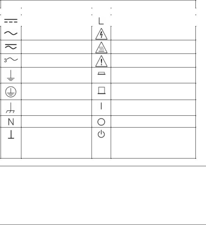
Safety Symbol Definitions
Symbol |
Description |
Symbol |
Description |
|
Direct current |
|
Terminal for Line conductor on permanently |
|
|
|
installed equipment |
Alternating current
Both direct and alternating current
Three-phase alternating current
Earth (ground) terminal
Protective earth (ground) terminal (Intended for connection to external protective conductor.)
Caution, risk of electric shock
Caution, hot surface
Caution (refer to accompanying documents)
In position of a bi-stable push control
Out position of a bi-stable push control
Frame or chassis terminal
Terminal for Neutral conductor on permanently installed equipment
Terminal is at earth potential (Used for measurement and control
circuits designed to be operated with one terminal at earth potential.)
On (supply)
Off (supply)
Standby (supply)
Units with this symbol are not completely disconnected from ac mains when this switch is off. To completely disconnect the unit from ac mains, either disconnect the power cord or have a qualified electrician install an external switch.
Notice
The information contained in this document is subject to change without notice. Agilent Technologies makes no warranty of any kind with regard to this material, including but not limited to, the implied warranties of merchantability, and fitness for a particular purpose.
Agilent Technologies shall not be liable for errors contained herein or for incidental or consequential damages in connection with the furnishing, performance or use of this material.
This document contains proprietary information which is protected by copyright. All rights are reserved. No part of this document may be photocopied, reproduced, or translated into another language without the prior written consent of Agilent Technologies.
ã Copyright 1993, 2000 Agilent Technologies, Inc.
Printing History
The edition and current revision of this manual are indicated below. Reprints of this manual containing minor corrections and updates may have the same printing date. Revised editions are identified by a new printing date. A revised edition incorporates all new or corrected material since the previous printing date.
First Edition ............ |
July, 1993 |
Second Edition ...... |
September, 2000 |
4
Table of Contents |
|
Introduction ............................................................................................................................................................................ |
7 |
Scope .................................................................................................................................................................................. |
7 |
Conventions Used In Text................................................................................................................................................... |
7 |
Manual Revisions................................................................................................................................................................ |
8 |
Safety Considerations ......................................................................................................................................................... |
8 |
Firmware Revisions ............................................................................................................................................................ |
8 |
Electrostatic Discharge ....................................................................................................................................................... |
8 |
Verification.............................................................................................................................................................................. |
9 |
Introduction......................................................................................................................................................................... |
9 |
Test Equipment Required.................................................................................................................................................... |
9 |
Measurement Techniques.................................................................................................................................................. |
11 |
Setup for Most Tests ...................................................................................................................................................... |
11 |
Electronic Load .............................................................................................................................................................. |
11 |
Current-Monitoring Resistor .......................................................................................................................................... |
11 |
Operation Verification Tests............................................................................................................................................. |
11 |
Performance Tests............................................................................................................................................................. |
11 |
Programming.................................................................................................................................................................. |
13 |
Constant Voltage (CV) Tests ......................................................................................................................................... |
13 |
CV Setup ..................................................................................................................................................................... |
13 |
Voltage Programming and Readback Accuracy .......................................................................................................... |
13 |
CV Load Effect ........................................................................................................................................................... |
14 |
CV Source Effect ........................................................................................................................................................ |
14 |
CV Noise (PARD)....................................................................................................................................................... |
14 |
Transient Recovery Time ............................................................................................................................................ |
15 |
Constant Current (CC) Tests .......................................................................................................................................... |
15 |
CC Setup ..................................................................................................................................................................... |
15 |
Current Programming and Readback Accuracy .......................................................................................................... |
15 |
Current Sink (CC-) Operation. .................................................................................................................................... |
16 |
CC Load and Line Regulation ..................................................................................................................................... |
16 |
CC Load Effect ........................................................................................................................................................... |
16 |
CC Source Effect......................................................................................................................................................... |
17 |
CC Noise (PARD)....................................................................................................................................................... |
17 |
Troubleshooting .................................................................................................................................................................... |
31 |
Introduction....................................................................................................................................................................... |
31 |
Test Equipment Required.................................................................................................................................................. |
31 |
Overall Troubleshooting ................................................................................................................................................... |
34 |
Power-On Self-Test........................................................................................................................................................... |
34 |
Signature Analysis ............................................................................................................................................................ |
35 |
Firmware Revisions (for Models 664xA & 665xA)....................................................................................................... |
41 |
Test Headers .................................................................................................................................................................. |
41 |
Troubleshooting Procedures ............................................................................................................................................. |
49 |
Flow Charts .................................................................................................................................................................... |
49 |
Bias and Reference Supplies .......................................................................................................................................... |
49 |
CV/CC Status Annunciators Troubleshooting................................................................................................................ |
49 |
Post Repair Calibration ..................................................................................................................................................... |
49 |
Inhibit Calibration Jumper ............................................................................................................................................. |
49 |
Calibration Password ..................................................................................................................................................... |
50 |
EEPROM Initialization ..................................................................................................................................................... |
66 |
Transferring Calibration Constants Into Factory Preset Locations ................................................................................... |
66 |
5
Disassembly Procedures ................................................................................................................................................... |
72 |
List of Required Tools ................................................................................................................................................... |
74 |
Top Cover, Removal & Replacement ............................................................................................................................ |
74 |
A2 GPIB Board, Removal & Replacement (for 664xA & 665xA Models Only) .......................................................... |
74 |
A2 Isolator Board, Removal & Replacement (for 654xA & 655xA Only) .................................................................... |
75 |
Front Panel Assembly, Removal and Replacement........................................................................................................ |
75 |
S1 Line Switch, Removal and Replacement................................................................................................................... |
76 |
A3 Front Panel Board, Removal and Replacement ........................................................................................................ |
76 |
A1 Main Board .............................................................................................................................................................. |
77 |
A4 Heatsink Assembly (500 Watt Models 6x5xA Only) ............................................................................................... |
77 |
A4A1 or A4A3 Left Tunnel Board, Removal and Replacement.................................................................................... |
78 |
A4A2 or A4A4 Right Tunnel Board .............................................................................................................................. |
78 |
B1 Fan, Removal and Replacement ............................................................................................................................... |
78 |
T1 Power Transformer, Removal and Replacement....................................................................................................... |
78 |
Principles of Operation ........................................................................................................................................................ |
81 |
Introduction....................................................................................................................................................................... |
81 |
I/O INTERFACE SIGNALS............................................................................................................................................. |
81 |
Overall Block Diagram (Figure 4-2) ................................................................................................................................. |
83 |
Detailed Block Diagram Discussion ................................................................................................................................. |
83 |
Secondary Interface Circuits (Figure 4-3) ...................................................................................................................... |
83 |
Output Power and Control Circuits (Figure 4-4)............................................................................................................ |
86 |
Output Power .............................................................................................................................................................. |
86 |
Control Circuits ........................................................................................................................................................... |
86 |
A3 Front Panel Board Circuits (Figure 4-5)................................................................................................................... |
89 |
A2 GPIB Board Circuits For Agilent Models 664xA and 665xA Only ......................................................................... |
90 |
Isolator Board Circuits for Agilent Models 654xA and 665xA Only (Figure 4-7) ........................................................ |
91 |
Replaceable Parts ................................................................................................................................................................. |
95 |
Introduction....................................................................................................................................................................... |
95 |
Chapter Organization ..................................................................................................................................................... |
95 |
Model Applicability ....................................................................................................................................................... |
95 |
How To Order Parts.......................................................................................................................................................... |
95 |
Diagrams ............................................................................................................................................................................. |
137 |
Introduction..................................................................................................................................................................... |
137 |
Interconnections.............................................................................................................................................................. |
137 |
AC Input and Transformer Connections ......................................................................................................................... |
137 |
Circuit Board Schematics................................................................................................................................................ |
137 |
Component Location Diagrams ...................................................................................................................................... |
137 |
Test Points ...................................................................................................................................................................... |
139 |
Manual Backdating Changes............................................................................................................................................. |
169 |
Index .................................................................................................................................................................................... |
173 |
6

1
Introduction
Scope
This manual contains information for troubleshooting and repairing four generic models of Agilent power supplies. The different power supply models described in this manual are listed in Table 1-1.
Note |
The information provided in this manual applies to all Agilent models listed in Table 1-1. Where |
|
differences exist among any of the models, these differences are explained in text. |
|
|
For installation, operation, programming, and calibration procedures, refer to the appropriate Operating Manual as listed in Chapter 2, Table 2-1. For information in determining the performance level of the power supply, either before or after repair, refer to Chapter 2, Verification. The functional circuit operation of the various Agilent models is described in Chapter 4. Replaceable parts lists and circuit diagrams are included in Chapters 5 and 6, respectively.
Table 1-1. Agilent Power Supplies Described In This Manual
Agilent Models |
200 Watt Models |
500 Watt Models |
GPIB |
Agilent 6641A-6645A |
Agilent 6651A-6655A |
Analog Programmable |
Agilent 6541A-6545A |
Agilent 6551A-6555A |
Conventions Used In Text
1.Power supply models can be divided into 200 watt and 500 watt models. A "4" in the third position of the model number indicates a 200 watt supply, while the digit "5" in the third position indicates a 500 watt unit.
2.In addition, power supplies can be divided according to GPIB supplies or Analog Programmable supplies. All GPIB models have a “6” in the second position of the model number, while Analog Programmable supplies have a “5” in the second position of the model number. The GPIB models include a GPIB board which permits communications between the supply and an external computer over the GPIB bus. Analog Programmable supplies use an Isolator Board instead of the GPIB board, and do not have the ability to communicate with an external computer.
3.When referring in text to either the 200 watt or 500 watt GPIB power supply models, the convention “models 664xA or 665xA,” respectively, is used. When referring to either the 200 watt or 500 watt nonGPIB (or Analog Programmable) models, the convention “models 654xA or 655xA,” respectively, is used.
4.In this manual all complementary signal names in text are shown with an asterisk (*) after the signal name. Example; PCLR*. In some schematic diagrams you may see a bar above the signal name, which is identical to the signal name shown in text with an asterisk.
Introduction 7
Manual Revisions
Agilent Technologies instruments are identified by a ten-character, serial number, such as, US36360101. This manual was written for power supplies with serial numbers equal to, or higher than, those shown on the title page.
If the serial number on the rear panel of your power supply is higher than the one on the title page, then the power supply was made after publication of this manual, and may have hardware and/or firmware differences not covered in this manual. If there are such differences, they are documented in one or more yellow “Manual Changes” sheets sent with the manual.
If the serial number of your power supply is below that listed on the title page, or if it uses an older serial number format such as 3023A-01456, then your power supply was made prior to those covered in this manual. If this is the case, refer to Appendix A for any backdating information that may apply.
Safety Considerations
This product is a Safety Class 1 instrument that has a protective earth terminal. Refer to the Safety Summary page at the beginning of this manual for general safety procedures and for the meaning of safety symbols appearing in the manual and on the power supply.
Hazardous voltages exist within the power supply chassis, at the output terminals, and at the programming terminals.
Firmware Revisions
The supply's firmware resides in the front panel board's ROM chip (A3U4), and in the main board's microprocessor chip (AlU504). For models 664xA and 665xA, firmware also resides in the GPIB board ROM chip (A2U106).
For GPIB models 664xA and 665xA, you can use the “*IDN?” query, as described in Chapter 3, to get the firmware revision numbers of your power supply's firmware. For Agilent models 654xA and 655xA, the revision number can be read from the label affixed atop the IC chip.
Electrostatic Discharge
The power supply has components that can be damaged by ESD (electrostatic discharge). Failure to observe standard antistatic practices can result in serious degradation of performance, even if complete failure does not occur.
When working on the power supply, observe all standard antistatic work practices. This includes, but is not limited to:
■Working at a static-free station, such as, a table covered with static-dissipative laminate or with an Agilent 9300-0797 conductive table mat.
■Using a conductive wrist strap, such as, an Agilent 9300-0969 or an Agilent 9300-0970 wrist strap.
■Grounding all metal equipment at the station to a single, common ground.
■Connecting low-impedance test equipment to static-sensitive components only when those components have power applied to them.
■Removing power from the power supply before removing, or installing, printed circuit boards.
8 Introduction
2
Verification
Introduction
This Chapter contains test procedures to verify that the Agilent Power Supply is operating normally. There are three types of tests as follows:
Test |
Description |
Built-In Self-Tests |
These tests are run automatically when the power supply is turned on. |
Operation Verification |
These tests verify that the power supply is operating normally but the tests |
|
do not check all specified operating parameters. |
Performance Tests |
These tests check that the supply meets all of the operating specifications |
|
as listed in the Operating Manual. |
Note |
The power supply must pass the built-in self-tests before the tests in this chapter can be performed. If the |
|
supply fails the self test, refer to the overall troubleshooting procedures in Chapter 3 of this manual. |
|
|
If any failures are encountered, or if abnormal test results are observed, refer to the Troubleshooting Procedures in Chapter 3 of this manual. The troubleshooting procedures will determine if repair and/or calibration is required. Calibration procedures are given in Appendix A of the appropriate Operating Manual.
Table 2-1. Applicable Agilent Power Supply Operating Manuals
For Agilent Model |
Operating Manual Part Number |
GPIB Models 664xA & 665xA |
5964-8267 |
Analog Programmable Models 654xA & 655xA |
5959-3374 |
Test Equipment Required
Table 2-2 lists the equipment required to perform the verification tests.
SHOCK HAZARD. The test should only be performed by qualified personnel. During the performance of these tests, hazardous voltages may be present at the output of the supply.
Verification 9

|
Table 2-2. Test Equipment Required for Verification |
||
|
|
|
|
Type |
|
Required Characteristics |
Recommended Model |
|
|
|
|
Current Monitor Resistor |
|
100 A (0.01 Ω) ±0.04% for Agilent |
Guildline 9230/100 |
|
|
6541A, 6551A, 6552A, 6641A, |
|
|
|
6651A, & 6652A models. |
|
|
|
15 A (0.1 Ω) ±0.04% for Agilent |
Guildline 9230/15 |
|
|
||
|
|
6542A, 6543A, 6544A, 6545A, |
|
|
|
6553A, 6554A, 6555A, 6642A, |
|
|
|
6643A, 6644A, 6645A, 6653A, |
|
|
|
6654A, 6655A models. |
|
|
|
|
|
DC Power Supply
Digital Voltmeter
Electronic Load
GPIB Controller1
Load Resistor
Oscilloscope
5 V @ 10 A
Resolution: 10 nV @ 1 V
Readout: 8 1/2 digits
Accuracy: 20 ppm
Voltage and current range must exceed range of supply under test. Power range: 250 W minimum
Full GPIB capabilities
0.1 Ω ±5%, 300 W for Agilent 6541A, 6641A, 6551A, 6651A, 6552A, 6652A models.
l.0 Ω ±5%, 300 W for Agilent 6542A, 6543A, 6544A, 6545A, 6553A, 6554A, 6555A, 6642A, 6643A, 6644A, 6645A, 6653A, 6654A, 6655A models.
Sensitivity: 1 mV Bandwidth Limit: 20 MHz Probe: 1:1 with RF tip
Agilent 66 Agilent 42A, 6653A
Agilent 3458A
Agilent N3300A mainframe with
Agilent N3306A (60 V) plug-in module or Agilent N3305A (150 V)
plug-in module.
Agilent 82350B
Ohmite C300KRlO
Ohmite C300KlRO
Agilent Infiniium
RMS Voltmeter
Variable-Voltage Transformer
1 For 664xA and 665xA models only.
True RMS Bandwidth: 20 MHz
Sensitivity: 100 μV
Adjustable from -13% to +6% of input range. Power: 1 kVA minimum.
Agilent 3400B
10 Verification
Measurement Techniques
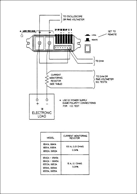
Setup for Most Tests
Most tests are performed at the rear terminals of the supply as shown in Figure 2-1. Measure the DC voltage directly at the +S and -S terminals. Set the output for remote sensing and use adequate wire gauge for the load leads as described in Chapter 4 of the Operating Manual.
Note |
All tests are performed as follows: Set the SENSE switch at the back of the supply to the Remote position. |
|
Connect the remote sensing leads from +OUT to +S, and from -OUT to -S. |
Electronic Load
Many of the test procedures require the use of a variable load capable of dissipating the required power. If a variable resistor is used, switches must be used to either; connect, disconnect, or short the load resistor. For most tests, an electronic load can be used. The electronic load is considerably easier to use than load resistors, but it may not be fast enough to test transient recovery time and may be too noisy for the noise (PARD) tests.
Fixed load resistors may be used in place of a variable load, with minor changes to the test procedures in this chapter. Also, if computer controlled test setups are used, the relatively slow (compared to computers and system voltmeters) settling times and slew rates of the power supply may have to be taken into account. "Wait" statements can be used in the test program if the test system is faster than the supply.
Current-Monitoring Resistor
To eliminate output-current measurement error caused by voltage drops in the leads and connections, connect the current monitoring resistor between the -OUT and the load as a four terminal device. Connect the current-monitoring leads inside the load-lead connections directly at the monitoring points on the resistor element.
Operation Verification Tests
To assure that the supply is operating properly, without testing all specified parameters, perform the following test procedures:
a.Perform the turn-on and checkout procedures given in Chapter 3 of the Operating Manual.
b.Perform the Voltage Programming and Readback Accuracy test, and the Current Programming and Readback Accuracy Performance test which are given in this chapter.
Performance Tests
Note |
A full Performance Test consists of those items listed as Specifications in Table 1-1 of the Operating |
|
Manual, that have a procedure in the Verification section of this chapter. |
|
|
The following paragraphs provide test procedures for verifying the supply’s compliance with the specifications listed in Table 1-1 of the Operating Manual. All of the performance test specifications are listed in the appropriate Performance Test Record Form for your specific model. You can record the actual measured values in the column provided in this form.
Verification 11
(CV TESTS)
(CV TESTS)
Figure 2-1. Basic Test Setup
12 Verification

Programming
You can program the supply from the front panel keyboard or from a GPIB controller (for models 664xA and 665xA) when performing the tests. The test procedures are written assuming that you know how to program the supply either; remotely from a GPIB controller (for 664xA and 665xA models), or locally using the control keys and indicators on the supply’s front panel. For models 654xA and 655xA you must use the front panel. Complete instructions on remote and local programming are given in the Operating Manual.
Constant Voltage (CV) Tests
CV Setup
If more than one meter or if a meter and an oscilloscope are used, connect each to the terminals by a separate pair of leads to avoid mutual coupling effects. For constant voltage DC tests, connect only to +S and -S, since the unit regulates the output voltage that appears between +S and -S, and not between the (+) and (-) output terminals. Use coaxial cable or shielded two-wire cable to avoid noise pickup on the test leads.
Voltage Programming and Readback Accuracy
This test verifies that the voltage programming, GPIB readback (on 664xA and 665xA models), and front panel display functions are within specifications. Note that the values read back over the GPIB should be identical to those displayed on the front panel.
a.Turn off the supply and connect a digital voltmeter between the +S and the -S terminals as shown in Figure 2-1.
b.Turn on the supply and program the supply to zero volts and the maximum programmable current (see Table 2-3) with the load off.
c.Record the output voltage readings on the digital voltmeter (DVM) and the front panel display. The readings should be within the limits specified in the performance test record form for the appropriate model under CV PROGRAMMING @ 0 VOLTS. Also, note that the CV annunciator is on. The output current reading should be approximately zero.
d.Program the output voltage to full-scale (see Table 2-3).
e.Record the output voltage readings on the DVM and the front panel display. The readings should be within the limits specified in the performance test record form for the appropriate model under CV PROGRAMMING @ FULL SCALE.
Table 2-3. Voltage and Current Values
Agilent Model |
Full-Scale |
Max. Prog. |
Full-Scale |
Max. Prog. |
Max. Prog. |
|
Voltage |
Voltage |
Current |
Current |
Overvoltage |
|
|
200 Watt Supplies |
|
|
|
|
|
|
|
|
|
6541A, 6641A |
8 V |
8.190 V |
20 A |
20.475 A |
8.8 V |
6542A, 6642A |
20 V |
20.475 V |
10 A |
10.237 A |
22 V |
6543A, 6643A |
35 V |
35.831 V |
6 A |
6.142 A |
38.5 V |
6544A, 6644A |
60 V |
61.425 V |
3.5 A |
3.583 A |
66.0 V |
6545A, 6645A |
120 V |
122.85 V |
1.5 A |
1.535 A |
132 V |
|
|
500 Watt Supplies |
|
|
|
|
|
|
|
|
|
6551A, 6651A |
8 V |
8.190 V |
50 A |
51.188 A |
8.8 V |
6552A, 6652A |
20 V |
20.475 V |
25 A |
25.594 A |
22 V |
6553A, 6653A |
35 V |
35.831 V |
15 A |
15.536 A |
38.5 V |
6554A, 6654A |
60 V |
61.425 V |
9 A |
9.214 A |
66.0 V |
6555A, 6655A |
120 V |
122.85 V |
4 A |
4.095 A |
132 V |
Verification 13
CV Load Effect
This test measures the change in output voltage resulting from a change in output current from full load to no load.
a.Turn off the supply and connect the output as shown in Figure 2-1 with the DVM connected between the +S and -S terminals.
b.Turn on the supply and program the current to the maximum programmable value and the voltage to the full-scale value (see Table 2-3).
c.Adjust the load for the full-scale current (see Table 2-3) as indicated on the front panel display. The CV annunciator on the front panel must be on. If it is not, adjust the load so that the output current drops slightly.
d.Record the output voltage reading on the DVM connected to +S and -S.
e.Open the load and again record the DVM voltage reading.
The difference between the DVM readings in steps (d) and (e) is the load effect voltage, and should not exceed the value listed in the Performance Test Record Form for the appropriate model under CV LOAD EFFECT.
CV Source Effect
This test measures the change in output voltage that results from a change in AC line voltage from the minimum to maximum value within the line voltage specifications.
a.Turn off the supply and connect the AC power line through a variable voltage transformer.
b.Connect the output as shown in Figure 2-1 with the DVM connected between the +S and the -S terminals. Set the transformer to nominal line voltage.
c.Turn on the supply and program the current to the maximum programmable value and the output voltage to the full-scale value (see Table 2-3).
d.Adjust the load for the full-scale current value (see Table 2-3) as indicated on the front panel display. The CV annunciator on the front panel must be on. If it is not, adjust the load so that the output current drops slightly.
e.Adjust the transformer to 13% below the nominal line voltage (e.g., l04.4 Vac for a 120 Vac nominal line voltage input).
f.Record the output voltage reading on the DVM.
g.Adjust the transformer to 6% above the nominal line voltage (e.g., 127.2 Vac for 120 Vac nominal line voltage input).
h.Record the output voltage reading on the DVM.
The difference between the DVM reading in steps (f) and (h) is the source effect voltage and should not exceed the value listed in the Performance Test Record Form for the appropriate model under CV SOURCE EFFECT.
CV Noise (PARD)
Periodic and random deviations (PARD) in the output (ripple and noise) combine to produce a residual AC voltage superimposed on the DC output voltage. CV PARD is specified as the rms or peak-to-peak output voltage in a frequency range from 20 Hz to 20 MHz.
a.Turn off the supply and connect the output as shown in Figure 2-1 to an oscilloscope (AC coupled) between the (+) and the (-) terminals. Set the oscilloscope’s bandwidth limit to 20 MHz and use an RF tip on the oscilloscope probe.
b.Turn on the supply and program the current to the maximum programmable value and the output voltage to the full-scale value (see Table 2-3).
c.Adjust the load for the full-scale current value (see Table 2-3) as indicated on the front panel display.
d.Note that the waveform on the oscilloscope should not exceed the peak-to-peak limits in the Performance Test Record Form for the appropriate model under CV NOISE (PARD).
e.Disconnect the oscilloscope and connect an AC rms voltmeter in its place. The rms voltage reading should not exceed the RMS limits in the Performance Test Record Form for the appropriate model under CV NOISE (PARD).
14 Verification
Transient Recovery Time
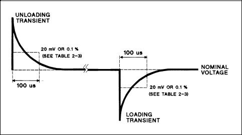
This test measures the time for the output voltage to recover to within the specified value following a 50% change in the load current.
a.Turn off the supply and connect the output as in Figure 2-1 with the oscilloscope across the +S and the -S terminals.
b.Turn on the supply and program the output voltage to the full-scale value and the current to the maximum programmable value (see Table 2-3).
c.Set the load to the Constant Current mode and program the load current to 1/2 the power supply full-scale rated current.
d.Set the electronic load’s transient generator frequency to l00 Hz and its duty cycle to 50%.
e.Program the load’s transient current level to the supply’s full-scale current value and turn the transient on.
f.Adjust the oscilloscope for a waveform similar to that in Figure 2-2.
g.The output voltage should return to within 0.1% or 20 mV, whichever is greater, of the nominal value in less than 100 microseconds. Check both loading and unloading transients by triggering on the positive and negative slope.
Figure 2-2. Transient Response Wavetorm
Constant Current (CC) Tests
CC Setup
Follow the general setup instructions in the Measurement Techniques paragraph and the specific instructions given in the following paragraphs.
Current Programming and Readback Accuracy
This test verifies that the current programming and readback are within specification. The accuracy of the current monitoring resistor must be 0.04% or better.
a.Turn off the supply and connect the current monitoring resistor across the output and a DVM across the resistor. See Current Monitoring Resistor.
b.Turn on the supply and program the output voltage to 5 V and the current to zero.
c.Divide the voltage drop (DVM reading) across the current monitoring resistor by its resistance to convert to amps and record this value (Iout). Also, record the current reading on the front panel display. The readings should be within the limits specified in the Performance Test Record Form for the appropriate model under CC PRGRAMMING @ 0 AMPS.
d.Program the output voltage to 5 V and the current to full-scale (see Table 2-3).
Verification 15
e.Divide the voltage drop (DVM reading) across the current monitoring resistor by its resistance to convert to amps and record this value (Iout). Also, record the current reading that appears on the front panel display. The readings should be within the limits specified in the performance test record form for the appropriate model under CC PROGRAMMING @ FULL-SCALE.
Current Sink (CC-) Operation.
This test verifies current sink operation and readback.
a.Turn off the supply and connect the output as shown in Figure 2-1, except connect a DC power supply in place of the electronic load as indicated.
b.Set the external power supply to 5 V and its current limit to 20% of the full scale current value (see Table 2-3) of the supply under test. For example, if the full scale current value is 25 A, set the external supply’s current limit to 5 A.
c.Turn on the supply under test and program the output voltage to zero. The current on the UUT display should be approximately 20% of the full-scale current.
d.Divide the voltage drop across the current monitoring resistor by its resistance to obtain the current sink value in amps and subtract this from the current reading on the display. The difference between the readings should be within the limits specified in the Performance Test Record Form for the appropriate model under, CURRENT SINK DISPLAY AND READBACK.
CC Load and Line Regulation
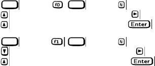
These tests (CC Load Effect and CC Source Effect given below) are tests of the DC regulation of the power supply’s output current. To insure that the values read are not the instantaneous measurement of the AC peaks of the output current ripple, several DC measurements should be made and the average of these reading calculated. An example of how to do this is given below using an Agilent 3458A System Voltmeter programmed from the front panel. Set up the voltmeter and execute the “Average Reading” program as follows:
a.Program 10 power line cycles per sample by pressing 

 .
.
b.Program 100 samples per trigger by pressing 

 .
.
c.Set up voltmeter to take measurements in the statistical mode as follows:
Press |
(shift key) |
(shift key) |
. |
|
Press |
until MATH function is selected, then press |
. |
||
Press |
until STAT function is selected, then press |
|
. |
|
d.Set up voltmeter to read the average of the measurements as follows:
Press |
(shift key) |
(shift key) |
. |
|
Press |
until RMATH function is selected, then press |
. |
||
Press |
until MEAN function is selected, then press |
. |
||
e.Execute the program by pressing 

 .
.
f.Wait for 100 readings and then read the average measurement by pressing  .
.
To repeat the measurement, perform steps (e) and (f).
CC Load Effect
This test measures the change in output current for a change in the load from full scale output voltage to short circuit.
a.Turn off the supply and connect the output as shown in Figure 2-1 with the DVM connected across the current monitoring resistor.
16 Verification
b.Turn on the supply and program the current to the full scale current value and the output voltage to the maximum programmable voltage value (see Table 2-3).
c.Adjust the load in the CV mode for full scale voltage as indicated on the front panel display. Check that the CC annunciator is on. If it is not, adjust the load so that the output voltage drops slightly.
d.*Record the output current reading (DVM reading/current monitor resistance value in ohms).
e.*Short the load switch and record the output current reading.
The difference in the current readings in steps (d) and (e) is the load effect and should not exceed the limit specified in the Performance Test Record Form for the appropriate model under CC LOAD EFFECT.
* You may want to use the average reading program described previously.
CC Source Effect
This test measures the change in output current that results when the AC line voltage changes from the minimum to the maximum value within the specifications.
a.Turn off the supply and connect the AC power line through a variable voltage transformer.
b.Connect the output terminals as shown in Figure 2-1 with the DVM connected across the current monitoring resistor. Set the transformer to the nominal line voltage.
c.Turn on the supply and program the current to the full scale value and the output voltage to the maximum programmable value (see Table 2-3).
d.Adjust the load in the CV mode for full scale voltage as indicated on the front panel display. Check that the CC annunciator is on. If it is not, adjust the load so that the output voltage drops slightly.
e.Adjust the transformer to 13% below the nominal line voltage.
f.*Record the output current reading (DVM reading/current monitoring resistor in ohms).
g.Adjust the transformer to 6% above the nominal line voltage.
h.*Record the output current reading again.
The difference in the current readings in steps (f) and (h) is the CC source effect and should not exceed the values listed in the Performance Test Record Form for the appropriate model under CC SOURCE EFFECT.
*You may want to use the average reading program described previously.
CC Noise (PARD)
Periodic and random deviations (PARD) in the output (ripple and noise) combine to produce a residual AC current, as well, as an AC voltage superimposed on the DC output. Constant current (CC) PARD is specified as the rms output current in a frequency range 20 Hz to 20 MHz with the supply in CC operation.
a.Turn off the supply and connect the load resistor and rms voltmeter as shown in Figure 2-3. Leads should be as short as possible to reduce noise pick-up. Use only a resistive load for this test.
b.Check the test setup for noise with the supply turned off. Other equipment (e.g. computer, DMM, etc.) may affect the reading.
c.Turn on the supply and program the current to full scale and the output voltage to the maximum programmable value (see Table 2-3).
d.The output current should be at the full scale rating with the CC annunciator on.
e.Divide the reading on the rms voltmeter by the load resistance to obtain rms current. It should not exceed the values listed in the Performance Test Record Form for the appropriate model under CC NOISE (RMS).
Verification 17

Figure 2-3. CC RMS Noise Measurement Test Setup
18 Verification

Table 2-4. Performance Test Record Form
Test Facility:
__________________________________________ |
Report No.__________________________________________ |
__________________________________________ |
Date______________________________________________ |
__________________________________________ |
Customer___________________________________________ |
__________________________________________ |
Tested By___________________________________________ |
Model_____________________________________ |
Ambient Temperature__________________________________ |
Serial No.__________________________________ |
Relative Humidity_____________________________________ |
Options ___________________________________ |
Nominal Line Frequency (Hz)___________________________ |
Firmware Revision___________________________ |
|
Special Notes: |
|
____________________________________________________________________________________________
____________________________________________________________________________________________
____________________________________________________________________________________________
____________________________________________________________________________________________
____________________________________________________________________________________________
____________________________________________________________________________________________
____________________________________________________________________________________________
____________________________________________________________________________________________
____________________________________________________________________________________________
Test Equipment Used:
Description |
Model No. |
Trace No. |
Cal. Due Date |
||
1. |
AC Source |
________ |
___________ |
___________ |
|
2. |
DC Voltmeter |
________ |
___________ |
___________ |
|
3. |
RMS Voltmeter |
________ |
___________ |
___________ |
|
4. |
Oscilloscope |
________ |
___________ |
___________ |
|
5. |
Electronic Load |
________ |
___________ |
___________ |
|
6. |
Current Monitoring |
________ |
___________ |
___________ |
|
|
Shunt |
|
|
|
|
|
|
|
|
|
|
|
|
|
|
|
|
|
|
|
|
|
|
Verification 19

Table 2-5. Performance Test Record for Agilent Model 6541A or 6641A
MODEL Agilent _____________ |
|
|
|
|
|
Report No.______________ |
Date_____________________ |
||
|
|
|
|
|
Test Description |
Minimum |
Results |
Maximum |
|
|
Spec. |
* |
Spec. |
|
|
Constant Voltage Tests |
|
|
|
Voltage Programming |
|
|
|
|
and Readback |
|
|
|
|
|
|
|
|
|
Low Voltage (0 V) Vout
Front Panel Display Readback
High Voltage (8 V) Vout
Front Panel Display Readback
Load Effect
Source Effect
PARD (Ripple and Noise)
Peak-to-Peak
RMS
Transient Response Time
(at 100 μs)
Current Programming
and Readback
Low Current (0 A) Iout
Front Panel Display Readback
High Current (20 A) Iout
Front Panel Display Readback
Current Sink (4 A) Display Readback
PARD (Ripple and Noise)
RMS
-5 mV |
________mV |
+5 mV |
|
Vout - 6 mV |
________mV |
Vout + 6 mV |
|
7.9902 V |
_________V |
8.0098 V |
|
Vout - 11.6 mV |
_______mV |
Vout + 11.6 mV |
|
Vout - 1 mV |
_______mV |
Vout + 1 mV |
|
Vout - 0.5 mV |
_______mV |
Vout + 0.5 mV |
|
0 |
_______mV |
3 mV |
|
0 |
_______μV |
300 μV |
|
0 |
_______mV |
20 mV |
|
|
|
|
Constant Current Tests
-26 mA |
_______mA |
+26 mA |
|
Iout - 18 mA |
_______mA |
Iout + 18 mA |
|
+19.944 A |
_________A |
+20.056 A |
|
Iout - 48 mA |
_______mA |
Iout + 48 mA |
|
Isink - 54 mA |
_______mA |
Isink + 54 mA |
|
0 |
________mA |
10 mA |
|
|
|
|
Load Effect |
|
Iout - 1 mA |
________mA |
Iout + 1 mA |
|
Source Effect |
|
Iout - 1 mA |
________mA |
Iout + 1 mA |
|
|
|
||||
|
|
|
|
|
|
|
*Enter your test results in this column. |
|
|
||
20 Verification
Table 2-6. Performance Test Record for Agilent Model 6542A or 6642A
MODEL Agilent _____________ |
|
|
|
|
|
Report No.______________ |
Date_____________________ |
||
|
|
|
|
|
Test Description |
Minimum |
Results |
Maximum |
|
|
Spec. |
* |
Spec. |
|
|
Constant Voltage Tests |
|
|
|
Voltage Programming |
|
|
|
|
and Readback |
|
|
|
|
|
|
|
|
|
Low Voltage (0 V) Vout
Front Panel Display Readback
High Voltage (20 V) Vout
Front Panel Display Readback
Load Effect
Source Effect
PARD (Ripple and Noise)
Peak-to-Peak
RMS
Transient Response Time
(at 100 μs)
Current Programming
and Readback
Low Current (0 A) Iout
Front Panel Display Readback
High Current (10 A) Iout
Front Panel Display Readback
Current Sink (2 A) Display Readback
PARD (Ripple and Noise)
RMS
Load Effect
-10 mV |
________mV |
+10 mV |
|
Vout - 15 mV |
________mV |
Vout + 15 mV |
|
19.978 V |
_________V |
20.022 V |
|
Vout - 29 mV |
_______mV |
Vout + 29 mV |
|
Vout - 2 mV |
_______mV |
Vout + 2 mV |
|
Vout - 0.5 mV |
_______mV |
Vout + 0.5 mV |
|
0 |
_______mV |
3 mV |
|
0 |
_______μV |
300 μV |
|
0 |
_______mV |
20 mV |
|
|
|
|
Constant Current Tests
-13 mA |
_______mA |
+13 mA |
||
Iout - 9.1 mA |
_______mA |
Iout + |
9.1 mA |
|
+ 9.972 A |
_________A |
+10.028 A |
||
Iout - 24.1 mA |
_______mA |
Iout + 24.1 mA |
||
Isink - 27 mA |
_______mA |
Isink + |
27 mA |
|
0 |
________mA |
5 mA |
||
Iout - 0.5 mA |
________mA |
Iout + |
0.5 mA |
|
|
|
|
|
|
Source Effect |
Iout - 0.5 mA |
________mA |
Iout + 0.5 mA |
|
|
|
|
*Enter your test results in this column.
Verification 21

Table 2-7. Performance Test Record for Agilent Model 6543A or 6643A
MODEL Agilent _____________ |
|
|
|
|
|
Report No.______________ |
Date_____________________ |
||
|
|
|
|
|
Test Description |
Minimum |
Results |
Maximum |
|
|
Spec. |
* |
Spec. |
|
|
Constant Voltage Tests |
|
|
|
Voltage Programming |
|
|
|
|
and Readback |
|
|
|
|
|
|
|
|
|
Low Voltage (0 V) Vout
Front Panel Display Readback
High Voltage (35 V) Vout
Front Panel Display Readback
Load Effect
Source Effect
PARD (Ripple and Noise)
Peak-to-Peak
RMS
Transient Response Time
(at 100 μs)
Current Programming
and Readback
Low Current (0 A) Iout
Front Panel Display Readback
High Current (6 A) Iout
Front Panel Display Readback
Current Sink (1.2 A) Display Readback
PARD (Ripple and Noise)
RMS
Load Effect
-15 mV |
________mV |
+15 mV |
|
Vout - 25 mV |
________mV |
Vout + 25 mV |
|
34.964 V |
_________V |
35.036 V |
|
Vout - 49.5 mV |
_______mV |
Vout + 49.5 mV |
|
Vout - 3 mV |
_______mV |
Vout + 3 mV |
|
Vout - 1 mV |
_______mV |
Vout +1 mV |
|
0 |
_______mV |
4 mV |
|
0 |
_______μV |
400 μV |
|
0 |
_______mV |
35 mV |
|
|
|
|
Constant Current Tests
-6.7 mA |
_______mA |
+6.7 mA |
|
Iout - 5 mA |
_______mA |
Iout + 5 mA |
|
+5.9843 A |
_________A |
+6.0157 A |
|
Iout - 14 mA |
_______mA |
Iout + 14 mA |
|
Isink -16.2 mA |
_______mA |
Isink +16.2 mA |
|
0 |
________mA |
3 mA |
|
Iout - 0.25 mA |
________mA |
Iout + 0.25 mA |
|
|
|
|
Source Effect |
Iout - 0.25 mA |
________mA |
Iout + 0.25 mA |
|
|
|
|
*Enter your test results in this column.
22 Verification

Table 2-8. Performance Test Record for Agilent Model 6544A or 6644A
MODEL Agilent _____________ |
|
|
|
|
|
Report No.______________ |
Date_____________________ |
||
|
|
|
|
|
Test Description |
Minimum |
Results |
Maximum |
|
|
Spec. |
* |
Spec. |
|
|
Constant Voltage Tests |
|
|
|
Voltage Programming |
|
|
|
|
and Readback |
|
|
|
|
|
|
|
|
|
Low Voltage (0 V) Vout
Front Panel Display Readback
High Voltage (60 V) Vout
Front Panel Display Readback
Load Effect
Source Effect
PARD (Ripple and Noise)
Peak-to-Peak
RMS
Transient Response Time
(at 100 μs)
Current Programming
and Readback
Low Current (0 A) Iout
Front Panel Display Readback
High Current (3.5 A) Iout
Front Panel Display Readback
Current Sink (0.7 A) Display Readback
PARD (Ripple and Noise)
RMS
Load Effect
-26 mV |
________mV |
+26 mV |
|
Vout - 40 mV |
________mV |
Vout + 40 mV |
|
59.938 V |
_________V |
60.062 V |
|
Vout - 82 mV |
_______mV |
Vout + 82 mV |
|
Vout - 4 mV |
_______mV |
Vout + 4 mV |
|
Vout - 1 mV |
_______mV |
Vout + 1 mV |
|
0 |
_______mV |
5 mV |
|
0 |
_______μV |
500 μV |
|
0 |
_______mV |
60 mV |
|
|
|
|
Constant Current Tests
-4.1 mA |
_______mA |
+4.1 mA |
|
Iout - 3 mA |
_______mA |
Iout + 3 mA |
|
+3.49065 A |
_________A |
+3.50935 A |
|
Iout - 8.25 mA |
_______mA |
Iout + 8.25 mA |
|
Isink - 9.25 mA |
_______mA |
Isink + 9.25 mA |
|
0 |
________mA |
1.5 mA |
|
Iout - 0.25 mA |
________mA |
Iout + 0.25 mA |
|
|
|
|
Source Effect |
Iout - 0.25 mA |
________mA |
Iout + 0.25 mA |
|
|
|
|
*Enter your test results in this column.
Verification 23

Table 2-9. Performance Test Record for Agilent Model 6545A or 6645A
MODEL Agilent _____________ |
|
|
|
|
|
Report No.______________ |
Date_____________________ |
||
|
|
|
|
|
Test Description |
Minimum |
Results |
Maximum |
|
|
Spec. |
* |
Spec. |
|
|
Constant Voltage Tests |
|
|
|
Voltage Programming |
|
|
|
|
and Readback |
|
|
|
|
|
|
|
|
|
Low Voltage (0 V) Vout
Front Panel Display Readback
High Voltage (120 V) Vout
Front Panel Display Readback
Load Effect
Source Effect
PARD (Ripple and Noise)
Peak-to-Peak
RMS
Transient Response Time
(at 100 μs)
Current Programming
and Readback
Low Current (0 A) Iout
Front Panel Display Readback
High Current (1.5 A) Iout
Front Panel Display Readback
Current Sink (0.3 A) Display Readback
PARD (Ripple and Noise)
RMS
Load Effect
-51 mV |
________mV |
+51 mV |
|
Vout - 80 mV |
________mV |
Vout + 80 mV |
|
119.877 V |
_________V |
120.123 V |
|
Vout - 164 mV |
_______mV |
Vout + 164 mV |
|
Vout - 5 mV |
_______mV |
Vout + 5 mV |
|
Vout - 2 mV |
_______mV |
Vout + 2 mV |
|
0 |
_______mV |
7 mV |
|
0 |
_______μV |
700 μV |
|
0 |
_______mV |
120 mV |
|
|
|
|
Constant Current Tests
-1.7 mA |
_______mA |
+1.7 mA |
|
Iout - 1.3 mA |
_______mA |
Iout + 1.3 mA |
|
+1.49605 A |
_________A |
+1.50395 A |
|
Iout - 3.55 mA |
_______mA |
Iout + 3.55 mA |
|
Isink - 3.95 mA |
_______mA |
Isink + 3.95 mA |
|
0 |
________mA |
1 mA |
|
Iout - 0.25 mA |
________mA |
Iout + 0.25 mA |
|
|
|
|
Source Effect |
Iout - 0.25 mA |
________mA |
Iout + 0.25 mA |
|
|
|
|
*Enter your test results in this column.
24 Verification

Table 2-10. Performance Test Record for Agilent Model 6551A or 6651A
MODEL Agilent _____________ |
|
|
|
|
|
Report No.______________ |
Date_____________________ |
||
|
|
|
|
|
Test Description |
Minimum |
Results |
Maximum |
|
|
Spec. |
* |
Spec. |
|
|
Constant Voltage Tests |
|
|
|
Voltage Programming |
|
|
|
|
and Readback |
|
|
|
|
|
|
|
|
|
Low Voltage (0 V) Vout
Front Panel Display Readback
High Voltage (8 V) Vout
Front Panel Display Readback
Load Effect
Source Effect
PARD (Ripple and Noise)
Peak-to-Peak
RMS
Transient Response Time
(at 100 μs)
Current Programming
and Readback
Low Current (0 A) Iout
Front Panel Display Readback
High Current (50 A) Iout
Front Panel Display Readback
Current Sink (10 A) Display Readback
PARD (Ripple and Noise)
RMS
Load Effect
-5 mV |
________mV |
+5 mV |
|
Vout - 6 mV |
________mV |
Vout + 6 mV |
|
7.9902 V |
_________V |
8.0098 V |
|
Vout - 11.6 mV |
_______mV |
Vout + 11.6 mV |
|
Vout - 1 mV |
_______mV |
Vout + 1 mV |
|
Vout - 0.5 mV |
_______mV |
Vout + 0.5 mV |
|
0 |
_______mV |
3 mV |
|
0 |
_______μV |
300 μV |
|
0 |
_______mV |
20 mV |
|
|
|
|
Constant Current Tests
-60 mA |
_______mA |
+60 mA |
|
Iout - 67 mA |
_______mA |
Iout + 67 mA |
|
+49.865 A |
_________A |
+50.135 A |
|
Iout - 142 mA |
_______mA |
Iout + 142 mA |
|
Isink -135 mA |
________mA |
Isink +135 mA |
|
0 |
________mA |
25 mA |
|
Iout - 2 mA |
________mA |
Iout + 2 mA |
|
|
|
|
Source Effect |
Iout - 2 mA |
________mA |
Iout + 2 mA |
|
|
|
|
*Enter your test results in this column.
Verification 25

Table 2-11. Performance Test Record for Agilent Model 6552A or 6652A
MODEL Agilent _____________ |
|
|
|
|
|
Report No.______________ |
Date_____________________ |
||
|
|
|
|
|
Test Description |
Minimum |
Results |
Maximum |
|
|
Spec. |
* |
Spec. |
|
|
Constant Voltage Tests |
|
|
|
Voltage Programming |
|
|
|
|
and Readback |
|
|
|
|
|
|
|
|
|
Low Voltage (0 V) Vout
Front Panel Display Readback
High Voltage (20 V) Vout
Front Panel Display Readback
Load Effect
Source Effect
PARD (Ripple and Noise)
Peak-to-Peak
RMS
Transient Response Time
(at 100 μs)
Current Programming
and Readback
Low Current (0 A) Iout
Front Panel Display Readback
High Current (25 A) Iout
Front Panel Display Readback
Current Sink (5 A) Display Readback
PARD (Ripple and Noise)
RMS
Load Effect
-10 mV |
________mV |
+10 mV |
|
Vout - 15 mV |
________mV |
Vout + 15 mV |
|
19.978 V |
_________V |
20.022 V |
|
Vout - 29 mV |
_______mV |
Vout + 29 mV |
|
Vout - 2 mV |
_______mV |
Vout + 2 mV |
|
Vout - 0.5 mV |
_______mV |
Vout + 0.5 mV |
|
0 |
_______mV |
3 mV |
|
0 |
_______μV |
300 μV |
|
0 |
_______mV |
20 mV |
|
|
|
|
Constant Current Tests
-25 mA |
_______mA |
+25 mA |
|
Iout - 26 mA |
_______mA |
Iout + 26 mA |
|
+24.9375 A |
_________A |
+25.0625 A |
|
Iout - 63.5 mA |
_______mA |
Iout + 63.5 mA |
|
Isink -61.5 mA |
_______mA |
Isink +61.5 mA |
|
0 |
________mA |
10 mA |
|
Iout - 1 mA |
________mA |
Iout + 1 mA |
|
|
|
|
Source Effect |
Iout - 1 mA |
________mA |
Iout + 1 mA |
|
|
|
|
*Enter your test results in this column.
26 Verification
Table 2-12. Performance Test Record for Agilent Model 6553A or 6653A
MODEL Agilent _____________ |
|
|
|
|
|
Report No.______________ |
Date_____________________ |
||
|
|
|
|
|
Test Description |
Minimum |
Results |
Maximum |
|
|
Spec. |
* |
Spec. |
|
|
Constant Voltage Tests |
|
|
|
Voltage Programming |
|
|
|
|
and Readback |
|
|
|
|
|
|
|
|
|
Low Voltage (0 V) Vout
Front Panel Display Readback
High Voltage (35 V) Vout
Front Panel Display Readback
Load Effect
Source Effect
PARD (Ripple and Noise)
Peak-to-Peak
RMS
Transient Response Time
(at 100 μs)
Current Programming
and Readback
Low Current (0 A) Iout
Front Panel Display Readback
High Current (15 A) Iout
Front Panel Display Readback
Current Sink (3 A) Display Readback
PARD (Ripple and Noise)
RMS
Load Effect
-15 mV |
________mV |
+15 mV |
|
Vout - 25 mV |
________mV |
Vout + 25 mV |
|
34.964 V |
_________V |
35.036 V |
|
Vout - 49.5 mV |
_______mV |
Vout + 49.5 mV |
|
Vout - 3 mV |
_______mV |
Vout + 3 mV |
|
Vout - 1 mV |
_______mV |
Vout +1 mV |
|
0 |
_______mV |
4 mV |
|
0 |
_______μV |
400 μV |
|
0 |
_______mV |
35 mV |
|
|
|
|
Constant Current Tests
-13 mA |
_______mA |
+13 mA |
|
Iout - 15 mA |
_______mA |
Iout + 15 mA |
|
+14.9645 A |
_________A |
+15.0355 A |
|
Iout - 37.5 mA |
_______mA |
Iout + 37.5 mA |
|
Isink -34.5 mA |
_______mA |
Isink +34.5 mA |
|
0 |
________mA |
5 mA |
|
Iout -0.5 mA |
________mA |
Iout + 0.5 mA |
|
|
|
|
Source Effect |
Iout - 0.75 mA |
________mA |
Iout + 0.75 mA |
|
|
|
|
*Enter your test results in this column.
Verification 27

Table 2-13. Performance Test Record for Agilent Model 6554A or 6654A
MODEL Agilent _____________ |
|
|
|
|
|
Report No.______________ |
Date_____________________ |
||
|
|
|
|
|
Test Description |
Minimum |
Results |
Maximum |
|
|
Spec. |
* |
Spec. |
|
|
Constant Voltage Tests |
|
|
|
Voltage Programming |
|
|
|
|
and Readback |
|
|
|
|
|
|
|
|
|
Low Voltage (0 V) Vout
Front Panel Display Readback
High Voltage (60 V) Vout
Front Panel Display Readback
Load Effect
Source Effect
PARD (Ripple and Noise)
Peak-to-Peak
RMS
Transient Response Time
(at 100 μs)
Current Programming
and Readback
Low Current (0 A) Iout
Front Panel Display Readback
High Current (9 A) Iout
Front Panel Display Readback
Current Sink (1.8 A) Display Readback
PARD (Ripple and Noise)
RMS
Load Effect
-26 mV |
________mV |
+26 mV |
|
Vout - 40 mV |
________mV |
Vout + 40 mV |
|
59.938 V |
_________V |
60.062 V |
|
Vout - 82 mV |
_______mV |
Vout + 82 mV |
|
Vout - 4 mV |
_______mV |
Vout + 4 mV |
|
Vout - 1 mV |
_______mV |
Vout + 1 mV |
|
0 |
_______mV |
5 mV |
|
0 |
_______μV |
500 μV |
|
0 |
_______mV |
60 mV |
|
|
|
|
Constant Current Tests
-8 mA |
_______mA |
+8 mA |
|
Iout - 7 mA |
_______mA |
Iout + 7 mA |
|
+8.9785 A |
_________A |
+9.0215 A |
|
Iout - 20.5 mA |
_______mA |
Iout + 20.5 mA |
|
Isink -21.3 mA |
_______mA |
Isink +21.3 mA |
|
0 |
________mA |
3 mA |
|
Iout - 0.5 mA |
________mA |
Iout + 0.5 mA |
|
|
|
|
Source Effect |
Iout -0.5 mA |
________mA |
Iout + 0.5 mA |
|
|
|
|
*Enter your test results in this column.
28 Verification

Table 2-14. Performance Test Record for Agilent Model 6555A or 6655A
MODEL Agilent _____________ |
|
|
|
|
|
Report No.______________ |
Date_____________________ |
||
|
|
|
|
|
Test Description |
Minimum |
Results |
Maximum |
|
|
Spec. |
* |
Spec. |
|
|
Constant Voltage Tests |
|
|
|
Voltage Programming |
|
|
|
|
and Readback |
|
|
|
|
|
|
|
|
|
Low Voltage (0 V) Vout
Front Panel Display Readback
High Voltage (120 V) Vout
Front Panel Display Readback
Load Effect
Source Effect
PARD (Ripple and Noise)
Peak-to-Peak
RMS
Transient Response Time
(at 100 μs)
Current Programming
and Readback
Low Current (0 A) Iout
Front Panel Display Readback
High Current (4 A) Iout
Front Panel Display Readback
Current Sink (0.8 A) Display Readback
PARD (Ripple and Noise)
RMS
Load Effect
-51 mV |
________mV |
+51 mV |
|
Vout - 80 mV |
________mV |
Vout + 80 mV |
|
119.877 V |
_________V |
120.123 V |
|
Vout - 164 mV |
_______mV |
Vout + 164 mV |
|
Vout - 5 mV |
_______mV |
Vout + 5 mV |
|
Vout - 2 mV |
_______mV |
Vout + 2 mV |
|
0 |
_______mV |
7 mV |
|
0 |
_______μV |
700 μV |
|
0 |
_______mV |
120 mV |
|
|
|
|
Constant Current Tests
- 4 mA |
_______mA |
+4 mA |
|
Iout - 3 mA |
_______mA |
Iout + 3 mA |
|
3.990 A |
_________A |
+4.010 A |
|
Iout - 9 mA |
_______mA |
Iout + 9 mA |
|
Isink -9.8 mA |
________mA |
Isink +9.8 mA |
|
0 |
________mA |
2 mA |
|
Iout - 0.5 mA |
________mA |
Iout + 0.5 mA |
|
|
|
|
Source Effect |
Iout - 0.5 mA |
________mA |
Iout + 0.5 mA |
|
|
|
|
*Enter your test results in this column.
Verification 29
 Loading...