


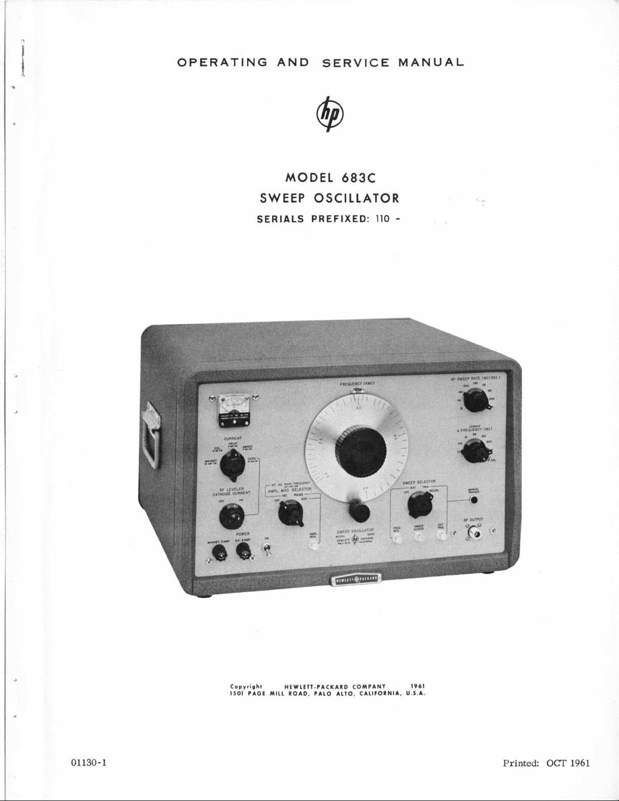
683C
3
P
!
OPERATING
AND
SERVICE
MANUAL
MODEL
6a3c
SWEEP OSCILLATOR
SERIALS PREFIXED:
J
110
-
01130-1
Copyright HEWLETT-PACKARD COMPANY
1501
PAGE
MILL
ROAD, PAL0
ALTO,
CALIFORNIA, U.S.A.
1961
Printed:
Om
1961
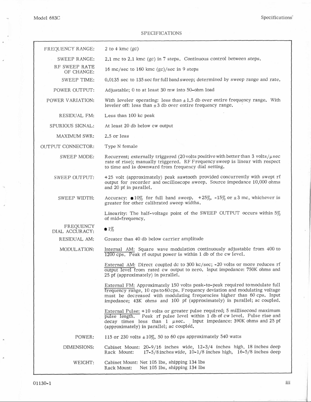
Model 683C Specifications’
SPECIFICATIONS
FREQUENCY RANGE:
SWEEP RANGE:
RF SWEEP RATE
OF CHANGE:
SWEEP TIME:
POWER OUTPUT:
POWER
SPURIOUS SIGNAL:
OUTPUT CONNECTOR:
VARIATION:
RESIDUAL FM:
MAXIMUM SWR:
SWEEP MODE:
SWEEP OUTPUT:
2 to 4 kmc (gc)
2.1 mc to 2.1 kmc (gc) in
16 mc/sec to 160 kmc (gc)/sec in 9 steps
0.0135
Adjustable;
With leveler operating:
leveler
Less than 100
At least 20 db below
2.5 or
Type N female
Recurrent; externally triggered (20 volts positive with better than 3 volts/psec
rate
to time and
+25 volt (approximately) peak sawtooth provided concurrently with swept
output for recorder and oscilloscope sweep. Source impedance 10,000 ohms
and 20 pf in parallel.
sec
to 135
sec
0
to
at least 30 mw into 50-ohm load
off:
less
than & 3 db over entire frequency range.
kc
peak
less
of
rise); manually triggered. RF Frequency sweep
is
downward from frequency dial setting.
7
steps. Continuous control between steps.
for full band sweep; determined by sweep range and rate.
less
cw
than f 1.5 db over
output
entire
frequency range.
is
.
linear with respect
With
rf
SWEEP WIDTH:
FREQUENCY
DIAL ACCURACY:
RESIDUAL AM:
MODULATION:
POWER:
Accuracy:
greater for other calibrated sweep widths.
Linearity: The half-voltage point of the SWEEP OUTPUT occurs within
of mid-frequency.
1%
Greater than 40 db below carrier amplitude
Internal
1200 cps. Peak
External AM: Direct coupled dc to 300 kc/sec; -20 volts or more reduces
output
25 pf (approximately) in parallel.
External FM: Approximately 150 volts peak-to-peak required to modulate full
frequency range, 10 cps to 60 cps, Frequency deviation and modulating voltage
be decreased with modulating frequencies higher than 60 cps. Input
must
impedance; 43K ohms and 100 pf (approximately) in parallel; ac coupled.
External Pulse:
pulse length.
decay times
(approximately) in parallel; ac coupl6d.
115 or 230 volts
AM:
level
10%
for full band sweep.
Square wave modulation continuously adjustable from 400 to
rf
output power
from rated
+
10 volts or greater pulse required: 5 millisecond maximum
Peak
less
f
lvo,
cw
rf
than 1 psec. Input impedance: 390K ohms and 25 pf
50
is
output to zero. Input impedance: 750K ohms and
pulse level within 1 db of
to 60 cps approximately 540 watts
+25%, -15% or
within 1 db of the
&
3
mc, whichever
cw
level.
cw
level. Pulse
rise
is
5%
rf
and
0
1130-
1
DIMENSIONS:
WEIGHT:
Cabinet Mount: 20-9/16 inches wide, 12-3/4 inches high, 18 inches deep
Rack Mount: 17-5/8inches wide,
Cabinet Mount: Net 105 lbs, shipping 134 lbs
Rack Mount:
Net
105 lbs, shipping 134 lbs
10-1/8
inches high, 16-5/8 inches deep
iii
Table of Contents
List of Tables
Model 683C
TABLE
Section Page
I
GENERAL INFORMATION
1.1
.
Description
1.2
.
Instrument Cooling System.
1.3
.
Three-Conductor Power Cable
1.4
.
1.5
1.6
I1
OPERATING INSTRUCTIONS
2.1
2.2
2.3
2.4
2.5
2.6
2.7
2.8
111
THEORY OF OPERATION
3-
3.2
3.3
3.4
3.5
3.6
3.7 . Helix Supply Reference Voltage and
3.8
3.9
230-Volt
.
Rack Mounting Instructions
.
BWOTube Information
.
Contents
.
Installation
.
Turn-On Procedure
Using the Sweep Oscillator
.
a CW Signal Source
.
Sweep Operation of the Oscillator
.
Amplitude Modulating the Oscillator
Frequency Modulating the Oscillator
.
.
Application
1
.
Contents
.
Backward-Wave Oscillator Tube
.
RF Leveler and Anode
Reference Circuit
.
Amplitude Modulator
.
Helix Modulator
.
Linear Sweep Generator
Exponential Voltage Generators
.
Regulated Power Supplies
.
Magnet Current Supply (Regulated)
...........
...
. .
Operation
.......
...
.....
............
...........
.......
as
......
.
..........
............
.
.......
......
.........
.....
.
....
1-1
1-1
1-1
1-2
1-2
1-3
2-
1
2-1
2-
1
2-2
2-2
2-2
2-2
2-8
3-
1
3-1
3-3
3-4
3-5
3-5
3-8
3-10
3-11
OF
CONTENTS
Section
IV
MAINTENANCE
4.1
.
General
4.2
.
General Precautions
4.3
4.4
4.5
4.6
4.7
4.8
4.10
4.11
4.12
4.13
4.14
4.15
4.16
4.17
4.18
4.19
4.20
4.21
V REPLACEABLE PARTS
5.1
5.2
Air Filter
.
.
Cabinet Removal
Quick-Check Procedure
.
.
Maintenance
Required
.
Magnet Supply (Regulated)
-150
.
.
Helix Supply
Filament Regulated
.
Measurement of Linear SweepTimes 4-9
.
Replacement
.
Calibration Procedure
RF Sweep Linearity
.
.
Square-Wave Generator
RF
.
Voltage Adjustment
.
Servicing the Sweep Circuits
Replacing Neon DC Coupling
.
Elements
Positioning Frequency Dial on
.
Potentiometer Shaft
.
Tube Replacement
.
Troubleshooting Procedure
.
Introduction
.
Ordering Information
...........
.....
..........
.......
....
Test
Equipment
.........
...
Volt Regulated Supply
.
..........
......
of
BWO Tube. and
...
.....
....
Leveler and Reference Anode
.....
. .
.........
.....
......
.
.........
.....
.
.
Page
c
4-1
4-1
4-2
4-2
4-2
4-6
4-6
4-7
4-7
4-9
4-10
4-14
4-15
4-15
4-17
4-19
4-19
4-22
4-22
5-1
5-1
iv
Number
1.1
.
Electronic Sweep Oscillators
3.1
.
Condition of
RF Sweep
4
.
1
.
Tube Replacement
4.2
.
Troubleshooting Procedure
5.1
.
Replaceable
Tubes
..
Parts
LIST
OF
TABLES
Title
........
During CW and
............
Chart
..........
.........
.............
Page
1-1
3-9
4 . 23
4-24
5-1
01130-1
Model 683C
LIST
OF
ILLUSTRATIONS
List of Illustrations
Number Title Page
1.1
.
2.1
2.2
2.3
2.4
2.5
2.6
2.7
2.8
2.9
2.10
3.1
3.2
3.3
3.4
3.5
3.6
3.7
3.8
3.9
Warranty Sheet
Turn-On Procedure and CW Operation
.
Using the Sweep Oscillator
.
as
a
Internal Sweep Modulation
.
Internal Square-Wave Modulation
.
External Pulse Modulation
.
External Amplitude Modulation
.
External Frequency Modulation
.
Allowable External Frequency
.
Suitable Setup for Measuring
.
Input and Output Connector
.
Backward- Wave Oscillator
.
Block Diagram Model 683C
.
RF
.
Adjustable Segments of
.
RF Leveler Circuit
.
Amplitude Modulation EXT
.
Frequency Modulator Waveforms
.
Simplified Schematic
.
Simplified Schematic of
.
CW Signal Source
Modulation Voltage Amplitude vs
Modulation Voltage Frequency
Frequency Deviation Limits when
using External FM
Characteristics
Tube Construction
Sweep Oscillator
Leveler Detected Waveform
(Leveled and Unleveled Positions)
Compensated Helix Voltage
Exponential Sweepcircuit
...........
.
.
.
.
.
2-2
2-3
2-4
2-5
2-6
2-7
2-8
2-9
2-10
3-1
3-2
3-3
3-3
3-4
3-5
3-6
3-7
3-8
......
......
...
......
....
....
...
........
..........
........
..........
....
.........
.
Position
...
of
Sweep Circuit
.....
1-2
2-0
Number
.
4.1
4.2
.
4.3
.
4.4
.
4.5
.
4.6
.
4.7
.
4.8
.
4.9
.
4.10
.
4.11
.
4.12
.
4.13
.
4.14
.
4.15
.
4.16
.
4.17
.
4.18
.
4.19
.
4.20
.
4.21
.
4.22
.
4.23
.
4.24
.
4.25
.
4.26
.
Title
Measuring RF Power Output
Checking Frequency Calibration and
General Performance
Setup for Measuring Residual AM
Measuring Magnet Circuit Ripple
Model 683C Top View
Sweep Output Voltage
Model 683C Bottom View
Model 683C Rear View
Positioning the BWO Tube at the
Front and Rear of Magnet
Calibration Pips on CRO Sweep
Example of Calibration Pips on
CRO Sweep
Crystal Detector-Attenuator
Response Curve
RF
Leveler Circuit Board
RF Leveler Calibration Setup
Model 683C Right Side View
Model 683C
Sweep Output Voltage Linearity
Troubleshooting Chart
Magnet Power Supply
(Current Regulated)
Regulated Primary Power and
Magnet Current Supply
Regulated +300 and -150 Volt PS
Frequency Supply and Low Voltage PS
RF Power Leveler and
Amplitude Modulator
Amplitude Modulator and Anode Section
Exponential and Linear Sweep Gen
Frequency (Helix) Modulator
............
Left
........
........
.........
.........
Side View
........
........
........
.....
.......
...
...
.......
......
....
......
.....
.....
......
....
.......
...
. .
.....
.
Page
4-2
4-3
4-5
4-7
4-8
4-9
4-12
4-12
4-13
4-14
4-15
4-16
4-18
4-19
4-20
4-21
4-22
4-28
4-30
4-31
4-32
4-33
4-34
4-35
4-36
4-37
01130-1
V
MODEL 683C
ELECTRONIC SWEEP OSCILLATOR
Model 683C
*
This manual specifically describes Model 683C of the
683C sweep oscillators. If, however, the serial number of your instrument
TllO
series, and
in
general describes all
is
prefixed by TO24
or T044, there are parts of themanual which do not apply to your instrument. If your instrument
carries one of these serial numbers, information specific to your instrument
is
furnished with
this manual. This supplementary material includes schematics, parts list, and replacement
paragraphs and illustrations for those items in the manual that do not describe your instrument.
The supplementary data
is
indexed; paragraph and figure numbers are the same as those used
in the manual for the corresponding information.
If
it
is
necessary to order replacement parts, consult the supplementary
the component
always
use
the part number in your supplementary parts list.
is
not listed,
use
the part number given in section V of the manual; otherwise,
parts
list first.
If
vi
01
130-
1
Model 683C
Paragraphs
Section
1-1
to
T
1-3
SECTION
GENERAL INFORMATION
1-1.
DESCRIPTION.
The @ Model 683C Sweep Oscillator
($3
Electronic Sweep Oscillators which
microwave bands as shown in table
Table 1-1. Electronic Sweep Oscillators
($9
Model
682C
683C
684C
H01
686C
686C
687C
Sweep oscillators are used as signal
wide variety of laboratory and production tests. They
provide a high-level relatively constant-amplitude
signal that can be rapidly changed in frequency. Thus
they permit the characteristics of microwave systems
or components to be quickly checked over an entire
band of frequencies.
The
@
Model 683C Sweep Oscillator covers the com-
plete
S
wave oscillator (bwo) tube to generate the
The bwo tube has several advantages over previously
used klystron type microwave oscillator tubes when
used in sweep sources.
The bwo tube output frequency and power level are
determined by the values of applied voltage only.
There are no cavity or reflector voltages to adjust or
track. There
lation. Since frequency and power-level adjustments
are electronic, all mechanical problems associated
with tunable-cavity Hystron-type oscillators are
inated. Control of frequency and power level are
simple, positive, and straightforward. By
rf
put from the bwo input, power variations of i1.5 db
are realized,
power from the bwo
full power from the bwo tube
output power
which
The Model 683C Sweep Oscillator
output can be either
internal square-wave source provides square-wave
modulation at any frequency between 400and 12OOcps.
The instrument can be externally pulse modulated or
band from 2 to 4 kmc (gc) and
is
no tendency to switch modes of oscil-
leveler circuit, which programs the
With
the
is
is
adjustable from 0 to a maximum
is
not
less
than 30 milliwatts.
cw
Frequency Range
1.0 to 2.0 kmc (gc)
2.0 to 4.0 kmc (gc)
4.0 to 8.1 kmc (gc)
7.0 to 11.0 kmc (gc)
8.2 to 12.4 kmc (gc)
12.4 to 18.0 kmc (gc)
rf
leveler inoperative, output
kept constant within 6 db, but
or amplitude modulated. An
is
one of several
cover
1-1.
sources
uses
a backward
rf
rf
power out-
is
obtained. The
is
versatile. The
signal.
use
major
for a
elim-
of
an
rf
I
amplitude modulated by
at any percentage from
oscillator can be externally frequency modulated or
swept
in
frequency over any portion or all
4-kmc (gc) range, or
taneously amplitude and frequency modulated.
When used for
lator, the internal circuitry provides an extremely
wide choice of sweeping rates and bandwidth swept.
The rate
and adjustable in calibrated steps from 16 mc/sec to
160 kmc(gc)/sec. The frequency range swept can be
small as 2.1 mc or as wide as 2.1 kmc (gc), as
as
selected by the calibrated seven position
QUENCY switch. In addition, there
control associated with the
which gives continuous adjustment between the fixed
positions
The minimum sweep time of the Model 683C
milliseconds. The sweep time
combined settings of the RF SWEEP RATE and the
A
FREQUENCY switches. These switches are inter-
locked by a differential gear drive which automatically
prevents any combination which would produce a sweep
time
less
The swept
linear with time and, by adjustment of
SELECTOR switch, can be made recurrent or
single sweeps. Single sweeps are started either by
the front-panel pushbutton or by an external positive
pulse (rise time greater than
In addition, a sawtooth voltage of approximately
25 volts
to supply a linear time base for an oscilloscope or
X-Y
recorder.
1-2.
INSTRUMENT COOLING SYSTEM.
The instrument
fan system. The incoming air
excessive dust. This filter must be inspected
quently to insure that it
dirty
filter
excessive heating of the instrument which can cause
early component failure (see figure 4-3).
1-3.
THREE-CONDUCTOR POWER CABLE.
To protect operating personnel, the National Electrical
Manufacturers’ Association (NEMA) recommends that
the instrument panel and cabinet be grounded. All
Hewlett-Packard instruments are equipped with a
three-conductor power cable which,
an appropriate receptacle, grounds the instrument.
The
offset pin
nector
is
its
primary purpose as a sweep oscil-
of
change of frequency
.
than 13.2 milliseconds.
rf
output frequency from the oscillator
is
provided concurrent with each
is
forced-air cooled by a high velocity
may restrict air flow sufficiently to cause
on
the power cable three-prongcon-
the ground pin.
sine
or complex waveforms
0
to
lOC%.
if
desired the 683C can be simul-
A
FREQUENCY switch
3
volts per microsecond).
is
is
not clogged with dirt.
In addition the
of
the 2- to
is
linear with time
A
is
a VERNIER
is
is
determined by the
the
SWEEP
set
rf
sweep
filtered to remove
when
plugged into
FRE-
13.2
is
for
fre-
A
0
1
130-
1
1-1
Section
Paragraphs
I
1-4
to 1-5
To preserve the protection feature when operating
the instrument from a two-contact outlet,
use
a threeprong to two-prong adapter and connect the green
pigtail on the adapter to ground.
1-4.
230-VOLT
The @ Model 683C
operation, but
OPERATION.
is
usually shipped wired for 115 vac
is
quickly and easily converted to
operation from a nominal 230-volt 50/60 cps source.
To convert, remove two jumpers between terminals
A2 and A3.
In
addition, remove the jumper
wire
(connecting the two rear terminals of the MAGNET
AMP and
3
minal of the
minal of
a pink lead attached to
either the MAGNET
the
H.
V.
3
AMP.
fuses)
from the rear
H.V.
fuse and reconnect to the side
H.V.
fuse.
This side terminal also has
it.
Do
not change the size of
fuse
or the
H.V.fuse.
ter-
ter-
When
operating from a 230-volt source, T101, the magnet
supply and the fan operate on 115 volts supplied by
T1
primary windings which act as a 2:l autotransformer. This additional load
load carried by the
sets
the expected reduction in current due to 230-volt
H.V.
is
added to the normal
fuse
and approximately off-
operation.
Model 683C
1-5.
RACK MOUNTING INSTRUCTIONS.
When mounting a rack model instrument, leave at
least three inches clearance behind the air intake to
insure
that the air intake
ment which
proper
is
air
circulation. In addition, be certain
is
not near another piece of equip-
discharging hot air
in
the
vicinity of
the Model 6836 air intake.
The following instructions should be followed for easy
installation of a rack model instrument (683CR)
in
an
equipment rack.
Remove the four
1)
screws
from
the
rear of the
in-
strument cabinet and slide the instrument forward
from the cabinet.
the
2) Mount
empty cabinet
four oval head machine
side
of
1-3/4
the cabinet
inches from the top and bottom edges of the
in
the
in
the equipment rack with
screws:
two
screws
on each
mounting holes approximately
mounting flanges.
3) Raise the instrument chassis and slide it gently
into the cabinet. Be certain the power cable passes
freely through the hole in the rear of the cabinet.
WARRANTY
CLAIM
AND
ADJUSIMINT PROCIDURI
MICROWAVE
INFORMATION
TUBE
WARRANTY CLAIM
Slp.t"re
Title
FORM
9/12/61
Figure
1-1.
Warranty Sheet
1-2 01130-1
Model 683C
4)
Fasten the instrument panel securely to the rack.
5)
Replace the four
(if
desired).
This instrument weighs over
If the rack installation
tion or rough handling, additional means of
support should be provided at the rear of
the instrument.
screws
Note
at the rear of the cabinet
100
pounds.
is
subject
to
vibra-
Section
Paragraph 1-6
1-6.
BWO
The bwo tube used in this instrument
and has a shorter guaranteed
tional tubes. See the Tube Warranty sheet, figure
for
details. A sheet for your
appendix of this manual. To
useful
suggested that the instrument be turned off when not in
use.
Wave Oscillator Tube Claims and Adjustment Pro-
cedure sheet in this manual should be read and the
instructions followed carefully.
hours of
When replacing the bwo tube, the Backward-
TUBE
service
INFORMATION.
is
very expensive
life
than that of conven-
use
is
increase
obtained from each tube, it
included in the
the number
1-1,
of
is
I
01130-1
Section I1
Figure 2-1
Model 6836
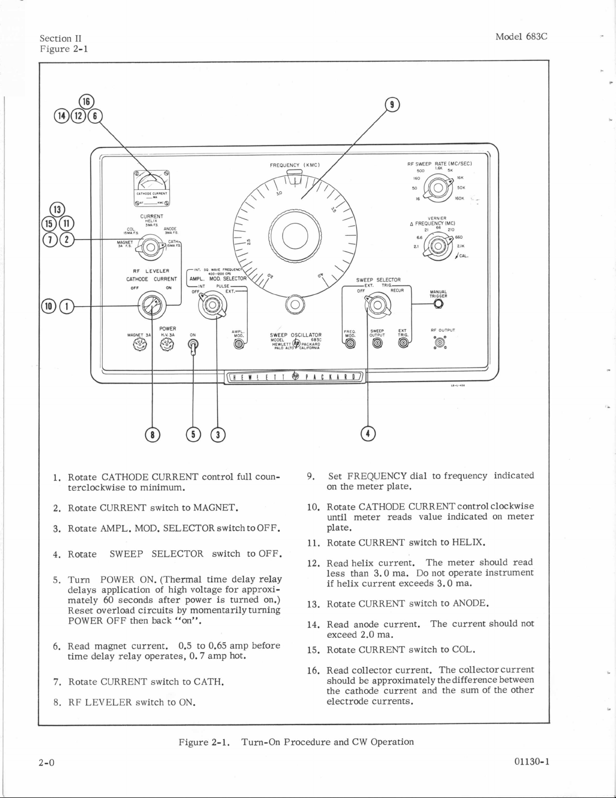
9.
1.
Rotate CATHODE CURRENT control
terclockwise to minimum.
2. Rotate CURRENT switch to MAGNET.
3. Rotate AMPL. MOD. SELECTOR switch toOFF.
4. Rotate SWEEP SELECTOR switch to
5. Turn POWER ON. (Thermal time delay relay
delays application of high voltage for approxi-
mately 60 seconds after power
Reset overload circuits by momentarily turning
POWER
6.
Read magnet current.
time delay relay operates,
7.
Rotate CURRENT switch to CATH.
8.
RF LEVELER switch to
2-0 01130-1
OFF
then back “on”.
0.5
to 0.65 amp before
0.7
amp hot.
ON.
Figure 2-1.
full
coun-
OFF.
is
turned on.)
Turn-On Procedure and CW Operation
Set FREQUENCY dial to frequency indicated
on the meter plate.
10. Rotate CATHODE CURRENT control clockwise
until meter reads value indicated on meter
plate.
11.
Rotate CURRENT switch to HELIX.
12. Read helix current. The meter should read
less
than
3.0
ma. Do not operate instrument
if
helix current exceeds
13.
Rotate CURRENT switch to ANODE.
14. Read anode current. The current should not
exceed 2.0 ma.
15.
Rotate CURRENT switch to COL.
16. Read collector current. The collector current
should be approximately the difference between
the cathode current and the sum of the other
electrode currents.
3.0
ma.
Model 683C
Paragraphs 2-1 to 2-3
Section I1
SECTION
OPERATING INSTRUCTIONS
2-1.
CONTENTS.
Section
operating the sweep oscillator, instructions for modulating the
cations of the instrument.
2-2.
The Model 683C Sweep Oscillator should be placed on
a work bench or table with at least 3 inches of clearance at
the filter. To avoid seriously restricted air flow,
be careful not to let loose pieces of paper, etc.
main in the rear area since they can be pulled against
the air filter.
The power cable should be used in a NEMA approved
standard three-prong grounding receptacle (paragraph 1-3).
Complete installation instruction for rack model
struments are given in paragraph 1-5.
2-3.
Good operating practice dictates that you follow ,a
given step-by-step procedure when turning on the
Model 683C, to protect the bwo tube. This routine
will
critical circuits to insure normal operation.
Under normal operation no damage can be done by
improper setting of front panel controls since builtin
high-voltage transformer
in
by momentarily turning off power to the instrument.
In addition to the overload protection, internal
driver-adjust controls preset limits on front panel
controls to safe values. BWO tube currents aremonitored with built-in metering circuits, which provide
a positive check that the bwo tube
in
To place the instrument in operation, the steps outlined
in
Additional data on some of the steps are given below
under STEPS; before performing the turn-on procedure
for the first time, read this supplemental information.
Figure 2-1 shows the front panel controls as
briefly describing the steps of the turn-on procedure.
The unnumbered controls and terminals can be oper-
ated in any order desired, depending on the type of
operation selected. Characteristics of the input and
output connectors are given
With the completion of the turn-on procedure the instrument
set
I1
contains instructions for setting up and
rf
output, and a discussion of some appli-
INSTALLATION.
the
rear to insure adequate air flow through
re-
in-
TURN-ON PROCEDURE.
systematically check out proper operation of all
overload protection cuts off primary power to the
if
excessive current flows
the helix circuit. The overload circuits are reset
screw-
is
being operated
a safe manner.
figure 2-1 should be followed in the order given.
well
as
in
figure 2-10.
is
set
up for
on the FREQUENCY dial. Once
cw
operation at the frequency
cw
operation has
II
been established, the oscillator may be adjusted for
frequency and for amplitude modulation (paragraphs
2-4 through 2-7).
Until thoroughly familiar with instrument operation,
it
is
recommended that you
information which follows.
STEPS:
The number associated with each paragraph
the turn-on procedure step under discussion. See
figure 2-1 for
5. Set POWER to ON. The plastic graticule at the
top of the FREQUENCY dial
fan
will
delays application of high voltage to the main
cuits approximately 60 seconds after
ment
are partly energized when the POWER switch
turned on, but do not regulate until the time-delay
switch has operated and the filaments
lator circuits are energized.
6. Read magnet current on the monitor meter. The
current should be 0.5 to 0.65 ampere when
turned on and
after a
ATE INSTRUMENT IF AFTER WARMUP THE
MAGNET CURRENT
AND
8.
With RF LEVELER switch to
have a power output variation across the band of
i1.5 db or
tion the power variation across the band will not
exceed
9.
It
is
cathode current at the frequency indicated on the
meter plate. The reasons are: a) Only with the
rated cathode current at the frequency specified
will
conditions are not met, the RF LEVELER
give the desired leveling action
10.Rotate CATHODE CURRENT control in a clock-
wise
Normal (at least 30 milliwatts) output
tained with the value of cathode current stamped
on the panel meter. (The maximum
limited by internal adjustments.)
12.Read helix current. The current should be
than 3 ma. DO NOT OPERATE THE INSTRUMENT IF THE HELIX CURRENT EXCEEDS 3MA.
An
overload relay prevents excessive helix
rent. To
POWER off, then back to ON. Excessive helix
current may indicate misalignment of the bwo tube
in
the magnetic field
the
steps not discussed below.
operate.
is
energized. The magnet supply
will
few
minutes operation. DO NOT OPER-
0.725
AMPERE.
less.
3
db.
important that the meter reads the exact
adequate power be produced. b) If the latter
direction and observe the current reading.
reset
refer
to the supplemental
refers
will
glow. The cooling
A
thermal time-delay switch
cir-
the
instru-
circuits
in
the regu-
first
gradually settle to 0.70 ampere
IS
NOT BETWEEN 0.675
ON
the 683C
In the RF LEVELER OFF posi-
(+
1.5 db).
will
current
will
be ob-
less
will
not
is
cur-
the relay, momentarily turn
(see
section IV, Maintenance).
to
is
01130-1
2-
1
I
Section
I1
Paragraphs 2-4 to 2-7
Verify proper operation of the helix power supply
by rotating the FREQUENCY dial from 2 to 4 kmc
(gc) and noting that there
current. (BWO
in
helix voltage.
helix
Thus
as the FREQUENCY dial
range
is
a check that helix voltage
16. The collector
ference
current
between cathode current and
the helix and anode current readings.
is
a variation
in
helix
current varies with a change
a variation
in
helix
is
turned through
is
current
its
changing.)
reading should be the dif-
the
sum of
If
there
is
a large difference between this value of collector
current and that shown by the meter,
ment
is
not functioning properly
The instrument
ting a 30 milliwatt or more
is
now operating normally and genera-
cw
signal at the frequency
(see
the
instru-
section
IV).
indicated by the FREQUENCY dial.
2-4.
ment is
the AMPL. MOD. SELECTOR switch
LEVELER to ON.
is
of better than
The output power level
USING THE SWEEP OSCILLATOR AS
A CW SIGNAL SOURCE.
Upon completion of the turn-on procedure, the
set
up for cw operation. However, check that
is
OFF; RF
In
cw operation, output frequency
indicated by the FREQUENCY dial to an accuracy
-+
1%.
is
adjustable from at least
instru-
30 milliwatts down to zero by theCATHODE CURRENT
control. Monitor
the power level near rated value to
ratings are not being exceeded.
higher than 7 ma
helix
current
to 7 ma and check that helix current
This
is
a
check
the bwo
is
discussed in paragraph 4-13B.)
the
cathode current when adjusting
insure
If
cathode current
is
required to get rated power, and
is
higher than 3 ma, set cathode
is
less
that tube
focus
is
correct.
that tube
current
than 3 ma.
(Focusing
By the addition of a precision attenuator, the 683C can
be used as a signal generator. Figure 2-2 indicates
connection of equipment for such a setup.
fraction of the power
SWEEP OSCILLATOR
POWER METER
lpw TO lOmw
2-4gc
in
@gyL
the line
THERMISTOR
MOUNT
Ipw
TO
2-
4gc
is
IOmw
A
20-db
coupled to the
DIRECTIONAL
COUPLER
I
-4gc
cdb .5db
Figure 2-2. Using the Sweep Oscillator
as a CW Signal Source
Model 683C
auxiliary arm of
The power-monitoring branch
iliary arm. Thus the
on the 431A Power Meter plus 20 db, and the
at the load
is
the
761D Dual Directional Coupler.
is
taken from this aux-
rf
power in the
line
is
the reading
rf
power
the monitored rfpower minus the setting
of the attenuator. The accuracy with which the power
reaching the load can be monitored in this way
is
limited by the accuracy of theattenuator. Rated accuracies of the other components are shown
2-5.
SWEEP OPERATION
OF
THE OSCILLATOR.
After the oscillator has been set up for
the
rf
output should
be
set
to the desired power level
in
figure 2-2.
cw
operation
and the FREQUENCY dial set to the proper setting.
Refer
to figure 2-3, for instructions on how to obtain
sweep operation.
2-6.
AMPLITUDE MODULATING
THE OSCILLATOR.
The 683C provides facilities for modulation with internally-generated square waves, externally-supplied
pulses (683C input, ac coupled), or externally supplied
voltages (683C input, dc coupled). Operation at various
positions of the switch are described
in
figures 2-5,
2-6, and 2-7.
2-7.
FREQUENCY MODULATING
THE OSCILLATOR.
The oscillator can be frequency-modulated from an
external source by placing the SWEEP SELECTOR
switch
in
the
EXT. position and applying a modulating
voltage to the FREQ. MOD. jack (figure 2-7). The
jack
is
ac coupled to an impedance of 43K shunted by
approximately 100 pf.
The bwo
rf
output frequency varies with respect to the
voltage at the input to the FREQ. MOD. jack from
approximately 8.2 mc/volt at 4 kmc (gc) to 23.8 mc/
volt at 2 kmc (gc). The full frequency band (2.1 kmc
[gcJ) may be swept (at a rate of between
10
to 60 cps)
by applying a voltage of 150 volts peak-to-peak to
the FREQ.
MOD.
jack. When sweeping full band,
the FREQUENCY dial should be set at approximately
3.2 kmc (gc). Frequency modulation
is
up and down
from the frequency indicated on the FREQUENCY dial.
Positive-going voltage applied to the FREQ. MOD.
iack increases the freauencv.
is
When the full band
swept, the frequency of the
modulation voltage should be within 10 and 60 cps.
When
the frequency of the modulation voltage
is
higher
than 60 cps, the band swept must be reduced to avoid
overload of the helix power supply.
The
chart shown
as figure 2-8 shows the maximum voltages which
should be applied to the FREQ. MOD. jack
when
mod-
ulating frequencies above 60 cps are used.
For external frequency modulation of the 683C, consideration must be given to the modulation character-
istics
voltage produces an exponential change
of the
of the bwo.
rf
output.
If
A
linear change
in
modulation
in
the frequency
small modulation voltages are used,
2-2
01130-1
Model 683C
COL
CURRENT
HELIX
,wr,
ANODE
RF
SWEEP
RATE
IMC/SECI
Section
Figure 2-3
-0
-0
I1
3A
POWER
H.V.
3A
MAGNET
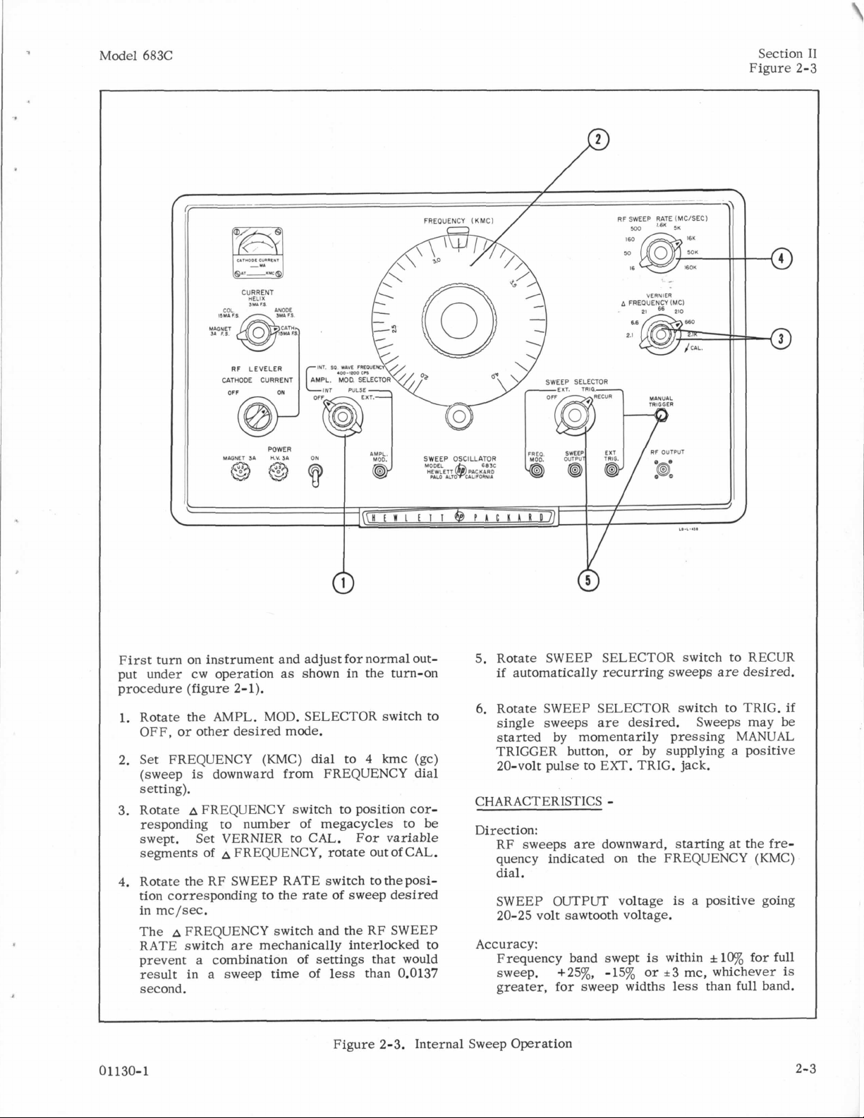
First turn on instrument and adjust for normal out-
put
under
cw
operation as shown in the turn-on
procedure (figure 2-1).
1.
Rotate the AMPL.
OFF,
or other desired mode.
2. Set FREQUENCY (KMC) dial to
(sweep
is
downward from FREQUENCY dial
MOD.
SELECTOR switch to
4
kmc (gc)
setting).
3.
Rotate A FREQUENCY switch to position cor-
responding to number of megacycles to be
swept. Set VERNIER to CAL. For variable
segments
4.
Rotate the RF SWEEP RATE switch totheposi-
of A FREQUENCY, rotate out of CAL.
tion corresponding to the rate of sweep desired
in mc/sec.
The
A
FREQUENCY switch and the RF SWEEP
RATE switch are mechanically interlocked to
prevent a combination
result in a sweep time of
of
settings that would
less
than 0.0137
second.
5.
Rotate SWEEP SELECTOR switch to RECUR
if
automatically recurring sweeps are desired.
6.
Rotate SWEEP SELECTOR switch to
TRIG.
single sweeps are desired. Sweeps may be
started by momentarily pressing MANUAL
TRIGGER button, or by supplying a positive
20-volt pulse to Em. TRIG. jack.
CHARACTERISTICS
-
Direction:
RF sweeps are downward, starting at the
quency indicated on the FREQUENCY (KMC)
dial.
SWEEP OUTPUT voltage
is
a positive going
20-25 volt sawtooth voltage.
Accuracy:
Frequency band swept
sweep. +25%, -15% or
greater, for sweep widths
is
within
i3
mc, whichever
less
f
10%
than full band.
for
if
fre-
full
is
O
1130-
~~
Figure 2-3. Internal Sweep Operation
1
2-3
Section
I1
Figure 2-4
Model 683C
RF
LEVELER
CATHODE CURRENT
FREQUENCY
(KMC)
RF SWEEP RATE (MCISECI
SW
5%
VERNIER
First turn on instrument and adjust
for
normal output under cw operation as shown in the turn-on
procedure (figure 2-1).
1.
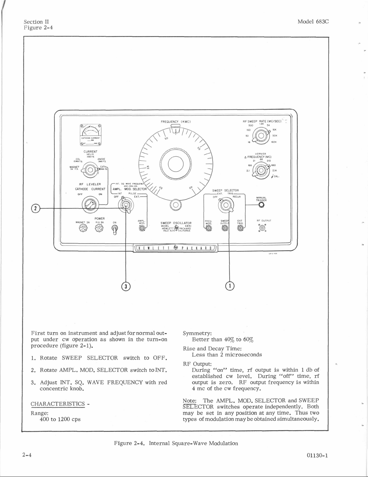
Rotate SWEEP SELECTOR switch to OFF.
2. Rotate AMPL. MOD. SELECTOR switch toINT.
3.
Adjust
INT.
SQ. WAVE FREQUENCY with red
concentric knob.
CHARACTERISTICS
-
Range:
400 to 1200 cps
Figure
2-4.
2-4
Symmetry:
Better than 4v0
Rise and Decay
Time:
Less than 2 microseconds
RF Output:
During "onyy time,
established
output
4
mc
of
cw
is
zero. RF output frequency
the
cw
frequency.
Note: The AMPL. MOD. SELECTOR and SWEEP
SELECTOR switches operate independently. Both
may be
types
set
in any position at any time. Thus two
of
modulation may be obtained simultaneously.
Internal Square-Wave Modulation
to
60%
rf
output
level. During
is
within 1 db
"off"
time,
is
within
01
of
rf
130-
1
Model 683C
Section
Figure 2-5
I1
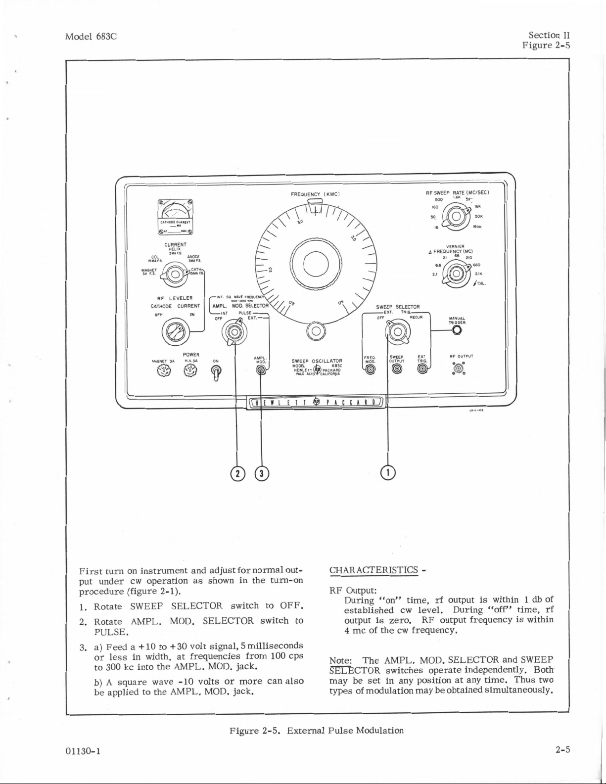
First turn on instrument and adjustfor normal output under
procedure (figure 2-1).
1.
Rotate SWEEP SELECTOR switch to OFF.
2. Rotate AMPL. MOD. SELECTOR switch to
PULSE.
3.
a) Feed
or
to
b)
be applied to the AMPL. MOD. jack.
01130-
1
cw
operation as shown in the turn-on
a
+
10
to
+30
volt signal, 5 milliseconds
less
in width, at frequencies from
300
kc into the AMPL. MOD. jack.
A
square wave
-10
volts
100
or
more can also
Figure 2-5. External Pulse Modulation
cps
CHARACTERISTICS
RF
Output:
During "on" time,
established
output
4
Note: The AMPL. MOD. SELECTOR and SWEEP
-
SELECTOR switches operate independently. Both
may be set in any position
types
is
zero. RF output frequency
mc
of
the cw frequency.
of
modulation may be obtained simultaneously.
-
rf
cw
level. During "off" time,
output
is
within 1 db
at
any time. Thus two
is
of
rf
within
2-5
Section
I1
Figure 2-6
RF
SWEEP RATE (MCISEC)
yI0
5x
Model 683C
CURRENT
HELIX
,udrs
COL
RF
CATHODE CURRENT
OFF
LEVELER
ANODE
3YA
@
31
POWER
n.v.m
MAGNET
16
FS
I601
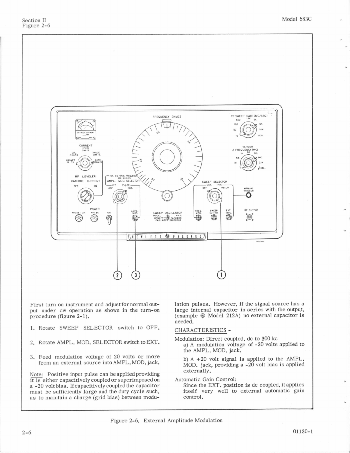
First turn on instrument and adjust for normal output under
procedure (figure 2-
cw
operation as shown
1).
in
the turn-on
lation pulses. However,
large internal capacitor in
(example
($9
Model 212A) no external capacitor
if
the signal source has a
series
with the output,
needed.
1.
Rotate SWEEP SELECTOR switch to OFF.
2. Rotate AMPL. MOD. SELECTOR switch to EXT.
CHARACTERISTICS
-
Modulation: Direct coupled, dc to 300 kc
a)
A
modulation voltage of -20 volts applied to
the AMPL. MOD. jack.
3.
Feed modulation voltage
from an external source into AMPL. MOD. jack.
Note:
-
Positive input pulse can be applied providing
it is either capacitively coupled or superimposed on
a -20 volt bias.
If
capacitively coupled the capacitor
must be sufficiently large and the duty cycle such,
as to maintain a charge (grid bias) between modu-
of
20 volts or more
b)
A
+20 volt signal
is
applied to the AMPL.
MOD. jack, providing a -20 volt bias
externally.
Automatic Gain Control:
Since the EXT. position
itself very
well
is
dc coupled,
to external automatic gain
control.
is
applied
it
applies
Figure 2-6. External Amplitude Modulation
2-6 01
is
130-
1
I
Model 683C
RF
LEVELER
CATHODE CURRENT
FREQUENCY (KMCI
RF SWEEP RAT€ IMCISEC)
VERNIER
Section
Figure 2-7
I1
31
POWER
H.V.3A
MAGNET
@@
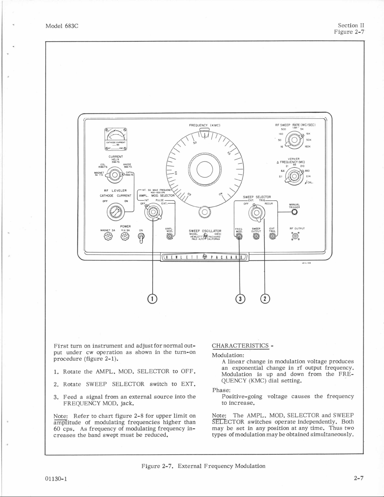
First
turn on instrument and adjust
put under
cw
operation as shown in the turn-on
procedure (figure 2-1).
Rotate the AMPL. MOD. SELECTOR
1.
2. Rotate SWEEP SELECTOR switch to EXT.
3.
Feed a signal from an external source into the
FREQUENCY MOD. jack.
for
normal out-
to
OFF.
CHARACTERISTICS
-
Modulation:
A
linear change in modulation voltage produces
an exponential change in
Modulation
is
up and down from the FRE-
rf
output frequency.
QUENCY (KMC) dial setting.
Phase:
Positive-going voltage causes the frequency
to increase.
Note: Refer to chart figure 2-8 for upper limit on
amplitude of modulating frequencies higher than
60 cps.
As
frequency
of
modulating frequency in-
creases the band swept must be reduced.
Figure
2-7.
01130-1
Note:
The AMPL. MOD. SELECTOR and SWEEP
SELECTOR switches operate independently. Both
may be
set
in any position at any time. Thus two
types of modulation may be obtained simultaneously.
External Frequency Modulation
2-7
Section 11
Model 683C
Paragraph 2-8
the
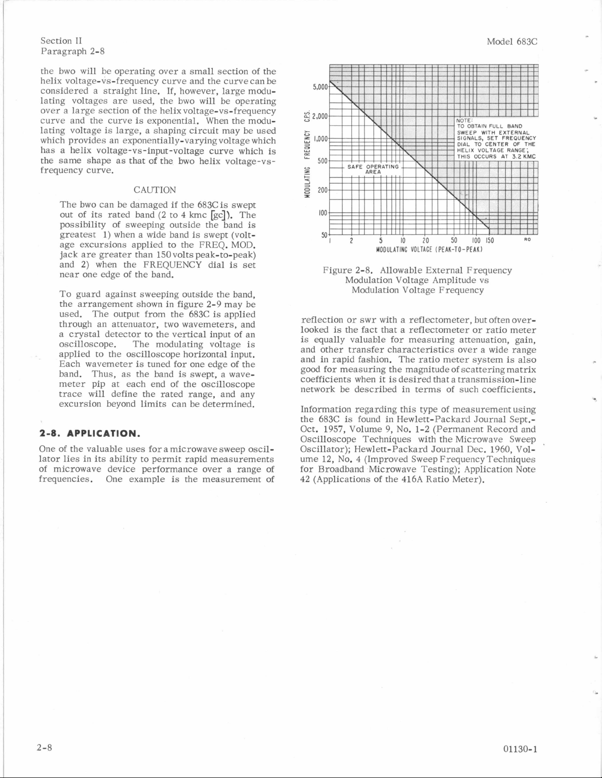
bwo will be operating over a small section of the
helix voltage-vs-frequency
considered a straight
curve
and the
line.
If, however, large modu-
curve
can be
lating voltages are used, the bwo will be operating
over a large section of the helix voltage-vs-frequency
curve and
lating voltage
the
curve
is
large, a shaping
is
exponential. When the modu-
circuit
may be used
which provides an exponentially-varying voltage which
has a helix
the same shape as that
voltage-vs-input-voltage
of
the bwo helix voltage-vs-
curve which
is
frequency curve.
CAUTION
The bwo can be damaged if
out of its rated band (2 to
possibility of sweeping outside
greatest 1) when a wide band
age excursions applied to the FREQ. MOD.
jack are greater than 150 volts peak-to-peak)
and
2)
when the FREQUENCY dial
near one edge of
the
band.
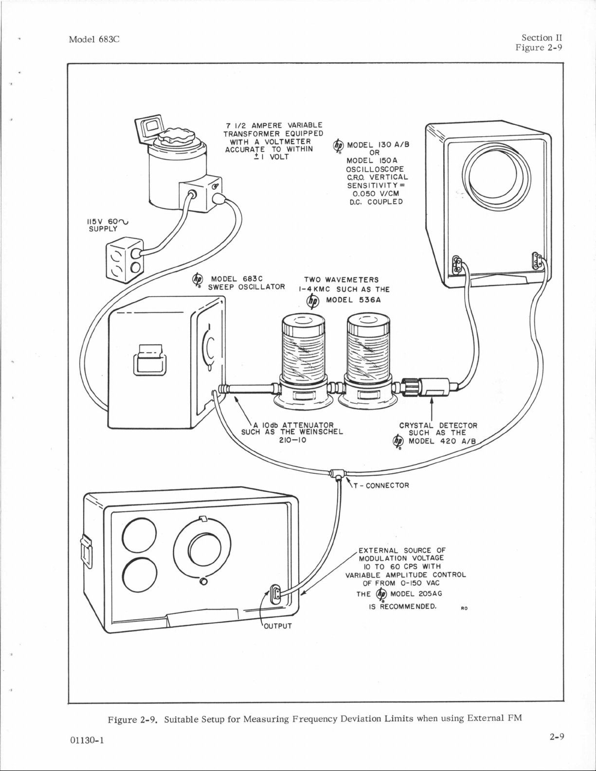
To guard against sweeping outside the band,
the arrangement shown
used. The output from
through an attenuator, two wavemeters, and
a crystal detector to the vertical input of an
oscilloscope. The modulating voltage
applied to the oscilloscope horizontal input.
Each wavemeter
band. Thus, as
is
tuned for one edge of the
the
meter pip at each end of the oscilloscope
trace will define the rated range. and any
excursion beyond limits can be ietermined.
2-8.
APPLICATION.
the
683Cis swept
4
kmc [gc]). The
is
swept (volt-
in
figure 2-9 may be
the
683C
band
is
swept, a wave-
the
is
band
is
set
applied
is
is
5
10
20
50
100
150
MODULATING VOLTAGE (PEAK-TO-PEAK)
RO
Figure 2-8. Allowable External Frequency
Modulation Voltage Amplitude
vs
Modulation Voltage Frequency
reflection or
looked
is
equally valuable for measuring attenuation, gain,
swr
with a reflectometer, but often over-
is
the fact that a reflectometer or ratio meter
and other transfer characteristics over a wide range
and
in
rapid fashion. The ratio meter system
is
also
good for measuring the magnitude of scattering matrix
coefficients when it
is
desired that a transmission-line
network be described in terms of such coefficients.
Information regarding this type of measurement using
the 683C
is
found in Hewlett-Packard Journal Sept.Oct. 1957, Volume 9, No. 1-2 (Permanent Record and
Oscilloscope Techniques with the Microwave Sweep
One of the valuable uses for a microwave sweep oscil- Oscillator); Hewlett-Packard Journal Dec. 1960, Vollator lies in its ability to permit rapid measurements ume 12, No.
4
(Improved Sweep Frequency Techniques
of microwave device performance over a range of for Broadband Microwave Testing); Application Note
frequencies.
One example
is
the measurement of 42 (Applications of
the
416A Ratio
Meter).
,
2-8
01130-1
Model
683C
7
1/2
AMPERE VARIABLE
TRANSFORMER €QUI PP ED
WITH A VOLTMETER
ACCURATE TO WITHIN
+I
VOLT
@
MODEL 150A
OSCILLOSCOPE
C.R.O. VERTICAL
SENSITIVITY
0.050
D.C. COUPLED
V/CM
A/B
=
Section
Figure 2-9
I1
SWEEP I-4-KMC
TWO WAVEMETERS
SUCH
AS THE
EXTERNAL SOURCE OF
MODULATION VOLTAGE
IO
TO
60
VARIABLE AMPLITUDE CONTROL
OF
IS
CPS WITH
FROM
0-150
MODEL 205AG
RECOMMENDED.
VAC
RO
11130-1
Figure
2-9.
Suitable Setup
for
Measuring Frequency Deviation Limits when using External FM
2-9
Section
Figure 2-10
I1
Model 683C
.
RF
OUTPUT
s
1.
PULSE
Ixto AMPL. MOD. jack
Input Pulse:
maximum length.
Impedance: 390K shunted by 25 pf.
EXT.
Input
to AMPL. MOD. jack dc
-20 volts
level to zero.
Impedance: 750K shunted by 25 pf, with diode
CR301
2. FREQ. MOD. Input: Positive pulse, 20 volts
Input Impedance:
approximately
+
10
or
more reduces
biased off.
100
volts or more; 5 milliseconds
ac coupled; 43K shunted by
pf.
is
ac coupled.
to
300
rf
level from cw
kc;
Frequency Response: Full band may be swept
10
cps
to
to avoid overload
chart figure 2-8 for limits at higher modulating
frequencies.
Sensitivity: 29.2 mc/volt at 2 kmc (gc) and
8.5 mc/volt at
3.
SWEEPOUTPUT
Output: 20-25 volts positive-slope sawtooth,
concurrent with
Internal Impedance:
4. EXT.TRIG.
time greater than
Impedance: 10K shunted by
60 cps, input voltage must be reduced
of
4
kmc (gc).
rf
output.
3
volts/psec.
power supplies. Refer to
10K
shunted by 20 pf.
10
pf.
or
more,
rise
2-10
Figure 2-
10.
Input and Output Connector Characteristics
01
130-
1
Model 683C
Paragraphs 3-1 to 3-2
Section
Ill
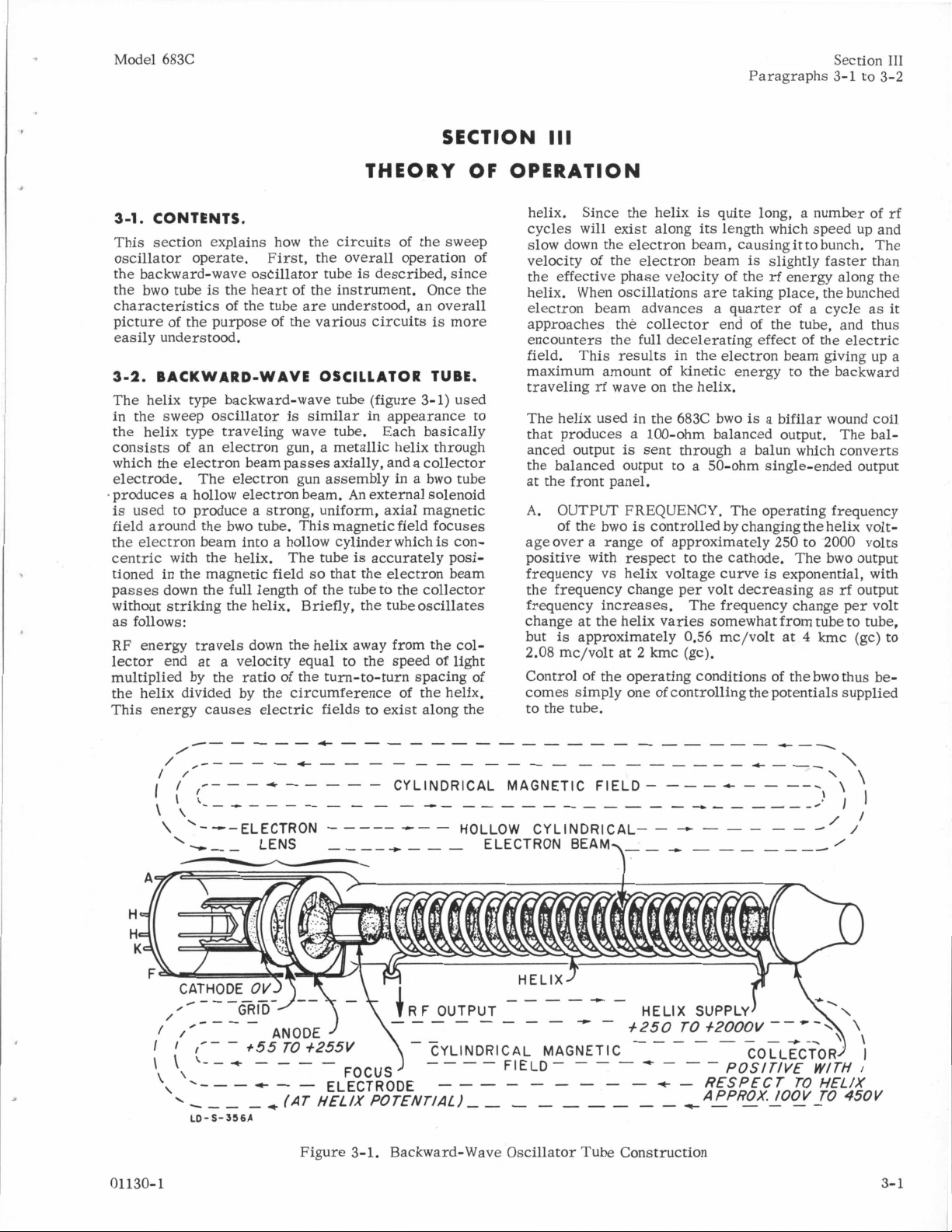
SECTION
THEORY
3-1.
CONTENTS.
This section explains how the circuits of the sweep
oscillator operate. First, the overall operation of
the backward-wave osCillator tube
the bwo tube
characteristics of the tube are understood, an overall
picture of the purpose of the various circuits
easily understood.
3-2.
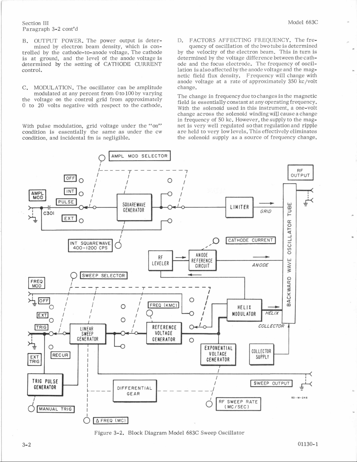
BACKWARD-WAVE OSCILLATOR TUBE.
The helix type backward-wave tube (figure 3in
the sweep oscillator
the helix type traveling wave tube, Each basically
consists of an electron gun, a metallic helix through
which the electron beam passes axially, and a collector
electrode. The electron gun assembly
.produces a hollow electron beam.
is
used to produce a strong, uniform, axial magnetic
field around the bwo tube. This magnetic field focuses
the electron beam into a hollow cylinder which
centric with the helix. The tube
tioned
passes down the full length of the tube to the collector
without striking the helix. Briefly, the tube oscillates
as follows:
RF energy travels down the helix away from the
lector end at a velocity equal to the speed of light
multiplied by the ratio of the turn-to-turn spacing of
the helix divided by the circumference of the helix.
This energy causes electric fields to exist along the
is
the heart of the instrument. Once
in
the magnetic field
is
similar
so
is
described, since
the
is
more
1)
used
in
appearance to
in
a bwo tube
An
external solenoid
is
con-
is
accurately posi-
that the electron beam
col-
111
OF
OPERATION
helix. Since the helix
cycles will exist along its length which speed up and
slow down the electron beam, causingit
velocity of the electron beam
the effective phase velocity of the
helix. When oscillations are taking place, the bunched
electron beam advances a quarter of a cycle as it
approaches
encounters the full decelerating effect of the electric
field. This results
maximum amount of kinetic energy to the backward
traveling
The helix used
that produces a 100-ohm balanced output.
anced output
the balanced output to a 50-ohm single-ended output
at the front panel.
A.
OUTPUT FREQUENCY. The operating frequency
of the bwo
ageover a range of approximately 250 to 2000 volts
positive with respect to the cathode.
frequency
the frequency change per volt decreasing as
frequency increases. The frequency change per volt
change at the helix varies somewhat from tube to tube,
but
is
2.08 mc/volt at
Control of the operating conditions of the bwo thus be-
comes simply one of controlling the potentials supplied
to the tube.
is
quite long, a number of
to
is
slightly faster than
rf
the
collector end of the tube, and thus
in
the electron beam giving up a
rf
wave on the helix.
in
the 683C bwo
is
sent through a balun which converts
is
controlled by changing the helix volt-
vs
helix voltage curve
approximately 0.56 mc/volt at 4 kmc (gc) to
2
kmc (gc).
is
a bifilar wound coil
is
bunch. The
energy along the
The bal-
The bwo output
exponential, with
rf
rf
output
01 130-
Figure 3-1. Backward-Wave Oscillator Tube Construction
3-
1
1
Section 111
Paragraph 3-2 cont’d
B.
OUTPUT POWER. The power output
mined by electron beam density, which
trolled by the cathode-to-anode voltage. The cathode
is
at
ground, and the level of the anode voltage
determined
control.
C. MODULATION. The oscillator can be amplitude
modulated at any percent from
the voltage on the control grid from approximately
0
to
With pulse modulation, grid voltage under the “on”
condition
condition, and incidental fm
by
the setting of CATHODE CURRENT
0
20 volts negative with respect
is
essentially the same
is
negligible.
AMPL
I
/-----
I
to
as
is
deter-
is
con-
100
by varying
to
the cathode.
under the cw
MOD
SELECTOR
r-------
I
I
is
Model 6836
D.
FACTORS AFFECTING FREQUENCY. The
quency
by the velocity
determined by the voltage difference between the cathode and the focus electrode. The frequency
lation
netic field flux density. Frequency will change with
anode voltage
change.
The change in frequency due
field
With the solenoid used in this instrument,
change
in frequency of
net
is
are
held
the solenoid supply
-7
I
01
of
oscillation
of
the electron beam. This in turn
is
alsoaffected by the anode voltageand the mag-
at
a
is
essentially constant
across
very well regulated
the solenoid winding will cause a change
50
kc. However, the supply
to
very low levels. This effectively eliminates
rate
as
of
the bwo tube
of
approximately
to
changes in the magnetic
at
any operating frequency.
is
to
so
that regulation and ripple
a
source
of frequency change.
determined
350
a
fre-
is
of
oscil-
kc/volt
one-volt
the mag-
.
>I
%
-
w
C301
I\
e.
.,
IEXTIO
Q
ISWEEP
LINEAR
SWEEP
GENE R ATOR GENERATOR
I
I
t
I
SELECTOR
SOUARE WAVE
GENERATOR
i
I
I
I--------
I
LEVELER
VOLTAGE
RF
I
I
“
---c
-
0
LIMITER
0
CATHODE
/
.
ANODE
REFERENCE
CIRCUIT
-1
I
41
EXPONENTIAL COLLECTOR
CURRENT
-
ANODE
I-
I
-W
GRID
1
m
~
3
IY
0
I-
U
-I
J
-
V
v)
0
W
>
4
0
U
a
s
Y
TRIG PULSE
It
GENERATOR
I
3-2
I
I
I
I
Figure 3-2. Block Diagram Model 683C Sweep Oscillator
SWEEP OUTPUT
ED-H-248
01130-1
Model 683C
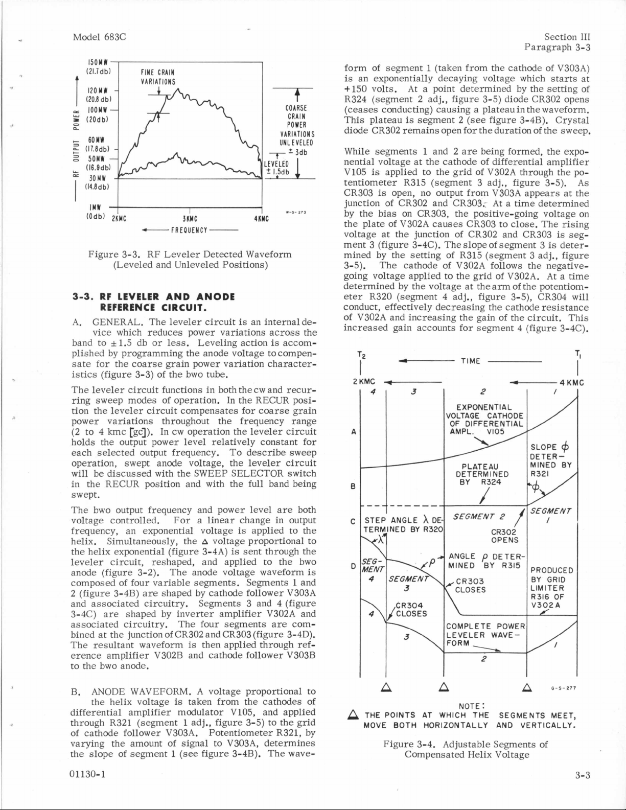
15OWW
(2I.Td b)
w
=
(20db)
0
@-
IWW
(Odb)
Figure 3-3.
3-3.
RF LEVELER
REFERENCE CIRCUIT.
A.
GENERAL. The leveler circuit
vice which reduces power variations across the
band to 1.5 db or
plished by programming the anode voltage to compensate for the coarse grain power variation characteristics (figure 3-3) of the bwo tube.
The leveler circuit functions
ring sweep modes of operation.
tion the leveler circuit compensates for coarse grain
power variations throughout the frequency range
(2 to 4 kmc [gc]).
holds the output power level relatively constant for
each selected output frequency. To describe sweep
operation, swept anode voltage, the
will be discussed with the SWEEP SELECTOR switch
in
the RECUR position and with the
swept.
The bwo output frequency and power level are both
voltage controlled. For a linear change in output
frequency, an exponential voltage
helix. Simultaneously, the
the
helix exponential (figure 3-4A)
leveler circuit, reshaped, and applied to the bwo
anode (figure 3-2). The anode voltage waveform
composed of four variable segments. Segments 1 and
2 (figure 3-4B) are shaped by cathode follower V303A
and associated circuitry. Segments 3 and 4 (figure
3-4C) are shaped by inverter amplifier V302A and
associated circuitry. The four segments are combined at the junction of CR302 and CR303 (figure 3-4D).
The resultant waveform
erence
to the bwo anode.
B. ANODE WAVEFORM.
differential amplifier modulator V105, and applied
through R321 (segment
of cathode follower V303A. Potentiometer R321, by
varying the amount of signal to V303A. determines
the slope of segment
amplifier V302B and cathode follower V303B
the helix voltage
FINE
GRAIN
-+-
Lx
2
1.5db
2KYC 3KWC 4KWC
-FREOUENCY
RF Leveler Detected Waveform
(Leveled and Unleveled Positions)
I
-
AND
ANODE
is
an internal de-
less.
Leveling action
in
both the
In the RECUR posi-
In
cw
operation the
A
voltage proportional to
is
then applied through
A
is
1
voltage proportional to
taken from the cathodes of
1
adj., figure 3-5) to the grid
(see
figure 3-4B). The wave-
leveler
leveler
full
is
is
sent through the
is
cw
and
band being
applied to the
COARSE
GRAIN
POWER
VARIATIONS
UNLEVELED
2
3db
*-I-
273
accom-
recur-
circuit
circuit
is
ref-
Section
Paragraph 3-3
form of segment
is
an exponentially decaying voltage which starts at
+I50 volts.
R324 (segment 2 adj., figure 3-5) diode CR302 opens
(ceases conducting) causing a plateau
This plateau
diode CR302 remains open for the duration of the sweep.
While segments
nential voltage at the cathode of differential amplifier
VI05
is
applied to the grid of V302A through the potentiometer R315 (segment 3 adj., figure 3-5).
CR303
junction of CR302 and CR303.r At a time determined
by the bias on CR303, the positive-going voltage on
the plate of V302A causes CR303 to close. The rising
voltage at the junction of CR302 and CR303
ment
mined by the setting of R315 (segment
3-5). The cathode of V302A follows the negativegoing voltage applied to the grid of V302A. At a time
determined by the voltage at thearm of the potentiom-
eter
conduct, effectively decreasing the cathode resistance
of V302A and increasing the gain of the circuit. This
increased gain accounts for segment
is
open, no output from V303A appears at the
3
(figure 3-4C). The slope of segment
R320 (segment 4 adj., figure 3-5), CR304
i'
2KMC
41
STEP ANGLE
EG-h
VENT
4
SEGMEN
1
(taken from the cathode of V303A)
At
a point determined by
is
segment 2
-
3
/p
1
and 2 are being formed, the expo-
(see
TIME
I
EXPONENTIAL
VOLTAGE CATHODE
OF DIFFERENTIAL
P LATE AU
DETERMINED
BY A324
1
MINED ANGLE
COMPLETE POWER
in
figure 3-4B).
4
-
2
CR302
OPENS
p
BY
DETER- R315
2
the
setting of
the waveform.
3
is
3
adj., figure
(figure 3-4C).
i
SLOPE
DETERMINED BY
SEGMENT
/
PRODUCED
BY GRID
LIMITER
R316 OF
V302A
111
Crystal
As
is
seg-
deter-
will
4
KMC
4
I
A
A
A
THE POINTS AT WHICH THE
MOVE BOTH HORIZONTALLY AND VERTICALLY.
Figure 3-4. Adjustable Segments of
Compensated Helix Voltage
a
NOTE
SEGMENTS MEET,
6-5-217
01130-1
3-3
Section 111
Paragraph 3-4
The composite waveform (figure 3-4D) at the junction
of CR302 and CR303 is applied to
fier
V302B.
reference
ampli-
C. REFERENCE AMPLIFIER V302B AND CATH-
ODE FOLLOWER V303B. Characteristically,
anode voltage
vs
power
level
(30 mw)
is
different
from one tube to another. Thus to obtain the power
level (30 mw) specified by
reference
the
purpose of
ply a variable dc
anode voltage must be variable. The
the
reference amplifier, V302B,
reference
the
bwo tubemanufacturer,
is
voltage between
to sup-
+55
and
+255 volts at the bwo anode.
Model 683C
D.
RF LEVELER OFF POSITION. When RF LEVELER switch S302 is in the
cathode of Y302B
is
placed at a dc reference by the
OFF
position, the
combined settings of R327, R332, and R335. The
purpose of the RF LEVELER OFF position
is
to make
available at certain frequencies higher power outputs.
Since
rf
leveling action
point, power output is sacrificed to obtain
is
referenced atthelow power
the
desired
leveling action.
3-4.
AMPLITUDE MODULATOR.
Resistor R327
is
a front panel control (CATHODE
CURRENT) that varies the bwo output power from
0
to 100%. The waveform at the plate of V302B
coupled to
which
the
grid of
in
turn applies the complete waveform to the
the
cathode follower V303B
is
dc
bwo anode. Degenerative feedback from the cathode
of V303B
is
applied to the grid of V302B through
R330 to reduce drift caused by tube aging andline
voltage variations.
i3OOV
(REG)
A
TO
CATHODE
VIOSA
OF
a
B
V302A
R320
20K
Y
RF LEVELER AND
REFERENCE ANODE CIRCUIT
1
Signals for amplitude-modulating the
applied to
the
control grid of the bwo tube, through the
rf
power are
amplitude modulator circuit. Voltage from the internal
400- to 1200-cps square-wave generator or signals
(pulse, square wave,
sine
wave, or complex wave)
from an external source may be used to modulate
the
rf
output. Condition of the amplitude modulator
circuit under various types of operation
is
discussed
briefly below.
FILAMENT ARRANGEMENT
PART
OF
et-
i
300
I33231
68
K
!&a24
V/REG)
IOOK
TI01
300
V
c
A0
(REG1
tl5OVIREG)
t-/
3-4
JEGMENT
JEGMENT
ADJUST
ADJUST
pam
R321
1
IM@
\e/
3V
(REG1
3V
(REG1
1
1
CATHODE
FOLLOW
E R
S302
?F
-CR302
vu
BALANCE
Figure 3-5. RF Leveler Circuit
Figure 3-5. RF Leveler Circuit
LEVEL.ER
ON
R333
15K
-fx)V
-fx)V
(REG)
(REG)
"?"
\
\
\
\
ICATHODE
ICATHODE
CURRENT]
CURRENT]
R331
IOOK
R332
R332
IOOK
IOOK
..
RO
RO
01130-1
Model 683C
A.
CW
OPERATION.
In
cw operation (AMPL.
MOD.
SELECTOR at OFF) diode CR301 clamps the bwo
control grid to ground. The
mined by the voltage on
rf
output level
the
anode, which
is
is
adjusted
deter-
by means of the CATHODE CURRENT control.
B.
INTERNAL SQUARE-WAVE OPERATION. With
the AMPL.
MOD.
SELECTOR on INT dual triode
V301 operates as a symmetrical free-running multivibrator. The frequency
mined
by
the charge and discharge time of C302 and
of
the
square wave
is
deter-
series-connected R303 and R302 (INT. SQ. WAVE FREQUENCY control). The symmetry of
is
set by adjusting (with
R3lO)
the
square wave
the dc bias on the
B
section of V301. The two adjustments are slightly
interdependent. The square-wave amplitude
is
clamped
to ground through crystal diode CR301. Thus the level
of the
rf
output during the “on”portionof the squarewave cycle corresponds to the cw level, set by the
CATHODE CURRENT control.
Paragraphs 3-5 to 3-6
Section
OUTPU
r
OF
TO
BWO
’5
R304
GRID
-
RO
Figure 3-6. Amplitude Modulation EXT. Position
Ill
C. PULSE OPERATION. With the AMPL.
SELECTOR switch on PULSE, the AMPL.
jack
is
connected, through capacitor C301, to the
grid of the
diode CR301
A
section of V301. Dual triode V301,
in
the plate circuit of
its
B
MOD.
MOD.
with
section,
is
operated as a limiting amplifier to provide constant
amplitude pulses to the control grid of the bwo tube.
The
A
section of V301
lower and the
B
Before an externally-supplied pulse
section of V301
is
through contacts on the AMPL.
switch,
is
tied to the control grid of the bwo tube; both
is
operated as a cathode fol-
section as a single-stage amplifier.
is
received,
the
conducting. The B-section plate,
MOD.
SELECTOR
are tied to the anode of diode CR301. With V301B conducting, the bwo tube
pulse, coupled by capacitor C301 to theV301Agrid,
is
cut off. The incoming positive
is
coupled to theV301 cathode, and turns off the B section.
The B-section plate rises, and
is
clamped
to
ground
through diode CR301. Thus during the “on” time of the
pulse, the level of the bwo
rf
output corresponds to the
cw level (set by the CATHODE CURRENT control).
The PULSE position
is
intended primarily
for
applications where low voltage pulses are available.
Pulses of
tion for faster pulsing characteristics
D.
volt source
20
volts or more can beused on EXT. posi-
EXTERNAL
MOD.
SELECTOR
is
(see
below).
AM
OPERATION. With the AMPL.
in
the Em. position the 300-
removed (see figure 3-6), eliminating
bias current to diode CR301. Thegridof the bwo tube
is
returned through a 1-megohm resistor R312 to
ground (figure 3-6) which permits application of posi-
tive input pulses provided
they
are either capacitively
coupled or superimposed on an externally supplied
-20
volt bias. The coupling capacitor must be
sufficiently large and the duty cycle such, soas to maintain a charge (grid bias) between modulation pulses.
Generally
very fast
modulating the bwo tube with a sine wave
the
external modulation facility
rise
time pulse modulation. Amplitude
is
used for
is
also
possible but introduces frequency pulling.
B
3-5.
HELIX MODULATOR.
The helix modulator (figure 4-22) consists of three
major sections:
the
linear sweep generator, the helix
supply reference voltage generator, and the exponential
voltage generator. The linear sweep generator generates:
1)
a precision time interval to start and stop
the exponential voltage generator thus determining the
time duration of the
sweep output voltage concurrent with the
sweep. The length of the precision time interval
rf
output sweep, and
2)
a linear
rf
output
is
governed by the settings of both the AFREQUENCY
and the RF SWEEP RATE controls.
The helix supply reference voltage generator determines the
rf
output frequency for cw operation and
the starting frequency for swept operation. The output of the reference voltage generator
adjustable by means of the FREQUENCY
which controls the setting
in
the cathode circuit of control tube V207A. The
of
variable resistor R236
is
continuously
(KMC)
dial
reference voltage generator determines frequency by
supplying the reference voltage for the regulated helix
supply and the regulated dc voltage for the exponential
voltage generator.
The exponential voltage generator produces an exponentially-varying voltage to drive the bwo helix for
internal sweep operation. Since the voltage-vs-time
curve
of the exponential generator
is
essentially
the
same shape as that of the bwo helix voltage-vsfrequency characteristic, the bwo produces a linear
rf
output sweep.
3-6.
LINEAR SWEEP GENERATOR.
The linear sweep generator consists of a Miller feed-
back integrator (V204A) which generates a linear
voltage sweep whose slope can be adjusted by changing
the charging rate
of
the integrator capacitor ((2207 to
C213). The AFREQUENCY (MC) range switch (part
of which
is
shown in figures 3-8 and 4-26) changes
the values of the integrator resistors (R230 to R232)
and capacitors (C207 to (2213) to obtain step changes
01130-1
3-5
Section
Figure
111
3-7
Model
683C
:N
I I !
v201
PIN
7
(0)
I
:
-1I5V
v201
PIN
1
(C)
I
;
-I14V,
'J
I
I
V208
PIN
9
(
rn)
s2-40v
V208
v202
I
PIN
7
DIODE
I
I
-25V.
-1ov'
,-23V
V204
PIN
(e)
3-6
8
;
I
t3T0
tt
fpTO
A
.-2.0
14
=
SWEEP TIME
lz1
15
RECOVERY AN0 HOLD-OFF TIME
FREOUENCY
,
NOTES
2.
I
KMC
-
SET RF SWEEP RATE
(-bp150A, WITH AC-2tA PROBE, DC COUPLED)
-
SET RF SWEEP RATE
WITH
VOLTMETER
TO
t6OKMC WHEN YEASURING WITH OSCILLOSCOPE
TO
16YC/SEC
(-hp-4lOB,
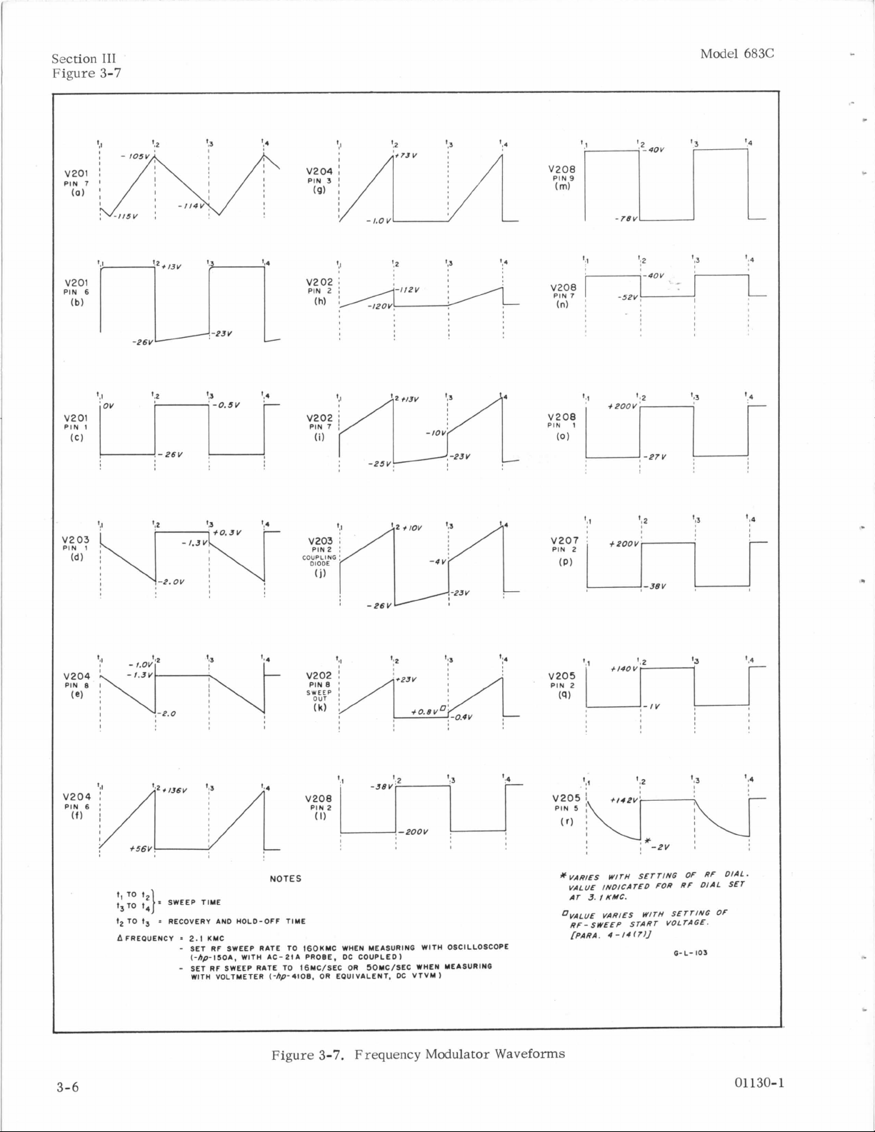
Figure
OR
OR
3-7.
SOMC/SEC WHEN MEASURlNO
EQUIVALENT, OC
Frequency Modulator
VTVM)
Waveforms
*VARIES
a~~~~~
WITH
f
KMC.
VARIES
4 - I4
SETTING
FOR
WITH
171J
RF
SETTING OF
G- L-
VALUE INDICATED
Ar
3.
RF-SWEEP START VOLTAGE.
[PARA.
OF
RF
DIAL
103
DIAL.
SET
01
130-
1
Model 683C
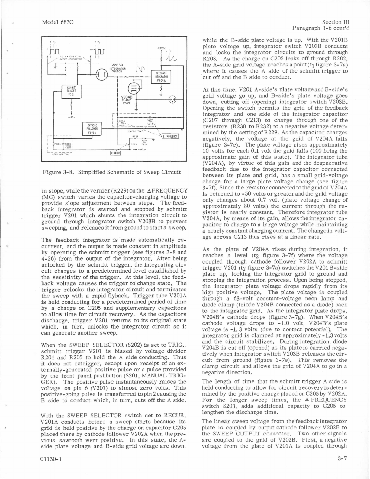
Paragraph 3-6 cont’d
Section
I11
Figure 3-8. Simplified Schematic of Sweep Circuit
in slope, while the
(MC) switch varies the capacitor-charging voltage to
provide slope adjustment between steps. The feedback integrator
trigger V201 which shunts the integration circuit to
ground through integrator switch V203B to prevent
sweeping, and releases
The feedback integrator
current, and the output
by operating the schmitt trigger
4-26) from the output of the integrator. After being
unlocked by the schmitt trigger, the integrating
cuit charges to a predetermined level established by
the sensitivity of the trigger.
back voltage causes the trigger to change state. The
trigger relocks the integrator circuit and terminates
the sweep with a rapid flyback. Trigger tube V201A
is
held conducting for a predetermined period of time
by a charge on C205 and supplementary capacitors
to allow time for circuit recovery.
discharge, trigger V201 returns to
which, in turn, unlocks the integrator circuit
can generate another sweep,
When the SWEEP SELECTOR (S202)
schmitt trigger V201
R204 and R205 to hold the
it does not retrigger, except upon receipt of an externally-generated positive pulse or a pulse provided
by the front panel pushbutton (S201, MANUAL TRIGGER). The positive pulse instantaneously raises the
voltage
positive-going pulse
B side to conduct which, in turn, cuts off the
With the SWEEP SELECTOR switch set to RECUR,
V201A conducts before a sweep starts because
grid
placed there by cathode follower V202A when theprevious sawtooth went positive. In this state, the
side plate voltage and B-side grid voltage are down,
on
is
held positive by the charge on capacitor C205
vernier
is
pin 6 (V201) to almost zero volts.
(R229) on the AFREQUENCY
started and stopped by schmitt
it
from ground to start a sweep.
is
made automatically
is
made constant in amplitude
(see
figures 3-8 and
At
this level, the feed-
As
the capacitors
its
original state
is
set to TRIG.,
is
biased by voltage divider
A
side conducting. Thus
is
transferred to pin 2 causing the
A
re-
cir-
so
This
side.
its
A-
it
while the B-side plate voltage
plate voltage up, integrator switch V203B conducts
and locks the integrator circuits to ground through
R208.
the A-side grid voltage reaches a point
where it causes the
cut off and the B side to conduct.
At this time, V201 A-side’s plate voltageand B-side’s
grid voltage go up, and B-side’s plate voltage goes
down, cutting off (opening) integrator switch V203B.
Opening the switch permits the grid of the feedback
integrator and one side of the integrator capacitor
(C207 through C213) to charge through one
resistors (R230 to R232) to a negative voltage determined by the setting of R229.
negatively, the voltage at the grid of V204A falls
(figure 3-7e). The plate voltage
10 volts for each 0.1 volt the grid falls (100 being
approximate gain of this state). The integrator tube
(V204A), by virtue of this gain and the degenerative
feedback due to the integrator capacitor connected
between its plate and grid, has a small grid-voltage
change for a large plate voltage change
3-7f). Since the resistor connected to the grid of V204A
is
only changes about 0.7 volt (plate voltage change of
approximately
sistor
V204A, by means of its gain, allows the integrator capacitor to charge to a large voltage while maintaining
a nearly constant charging current. The change in voltage across C213 thus
As
reaches a level (t2 figure 3-7f) where the voltage
coupled through cathode follower V202A to schmitt
trigger V201 (t2 figure 3-7a) switches theV201 B-side
plate up, locking the integrator grid to ground and
stopping the integration process. Upon being stopped,
the integrator plate voltage drops rapidly from
high positive voltage. The plate voltage
through a 63-volt constant-voltage neon lamp and
diode clamp (triode V204B connected as a diode) back
to the integrator grid.
V204B’s cathode drops (figure 3-7g). When V204B’s
cathode voltage drops to -1.0 volt, V204B’s plate
voltage
integrator grid
and the circuit stabilizes. During integration, diode
V204B
tively when integrator switch V203B releases the
cuit from ground (figure 3-7e). This removes the
clamp
negative direction.
The length of time that the schmitt trigger
held conducting to allow for circuit recovery
mined by the positive charge placed on C205 by V202A.
For the longer sweep times, the
switch S203, adds additional capacity to C205 to
lengthen the discharge time.
The linear sweep voltage from the feedback integrator
pl.ate
the SWEEP OUTPUT connector. Two other signals
are coupled to the grid of V202B. First, a negative
voltage from the plate of V201A
As
the charge on C205 leaks off through R202,
A
side of the schmitt trigger to
returned to -50 volts orgreaterand the grid voltage
80
volts) the current through the
is
nearly constant. Therefore integrator tube
rises
the plate of V204A
As
is
-1.3 volts (due to contact potential). The
is
clamped at approximately
is
cut
off
(opened) as
circuit
is
and allows the grid of V204A to go in a
coupled by output cathode follower V202B to
is
up. With the V201B
(ti
figure 3-7a)
of
As
the capacitor charges
rises
approximately
(see
figure
at a linear rate.
rises
during integration, it
is
coupled
the integrator plate drops,
-
1.3
volts
its
plateis carried nega-
A
side
is
deter-
A
FREQUENCY
is
coupled through
the
the
re-
its
cir-
is
0
1130- 1
3-
7
 Loading...