


 Loading...
T M 1 1 - 6 6 2 5 - 2 9 5 8 - 1 4 & P
TECHNICAL MANUAL
OPERATOR’S, ORGANIZATIONAL, DIRECT SUPPORT AND GENERAL SUPPORT
MAINTENANCE MANUAL
(INCLUDING REPAIR PARTS
AND SPECIAL TOOLS LIST)
FOR
POWER SUPPLY PP-7545/U
(HEWLETT-PACKARD MODEL 6269B) (NSN 6130-00-148-1796)
HEADQUARTERS, DEPARTMENT OF THE ARMY 21 AUGUST 1980
S A F E T Y I S T H E
S T E P S T O F O L L O W I F S O M E O N E V I C T I M O F E L E C T R I C A L S H O C K
D O N O T T R Y T O P U L L O R G R A B T H E I N D I V I D U A L
I F P O S S I B L E , T U R N O F F T H E E L E C T R I C A L P O W E R
I F Y O U C A N N O T T U R N O F F T H E E L E C T R I C A L
P O W E R , P U L L , P U S H , O R L I F T T H E P E R S O N T O
S A F E T Y U S I N G A W O O D E N P O L E O R A R O P E O R S O M E O T H E R I N S U L A T I N G M A T E R I A L
S E N D F O R H E L P A S S O O N A S P O S S I B L E
A F T E R T H E I N J U R E D P E R S O N I S F R E E O F
C O N T A C T W I T H T H E S O U R C E O F E L E C T R I C A L
S H O C K , M O V E T H E P E R S O N A S H O R T D I S T A N C E
A W A Y A N D I M M E D I A T E L Y S T A R T A R T I F I C I A L R E S U S C I T A T I O N

This manual includes copyright material reproduced by permission of the HEWLETT-PACKARD Company.
|
TM 11-6625-2958-14&P |
|
TECHNICAL MANUAL |
HEADQUARTERS |
|
|
||
No. 11-6625-2958-14&P |
DEPARTMENT OF THE ARMY |
|
Washington DC, 21 August 1980 |
||
|
O P E R A T O R ’ S , O R G A N I Z A T I O N A L , D I R E C T S U P P O R T A N D G E N E R A L S U P P O R T M A I N T E N A N C E M A N U A L (INCLUDING REPAIR PARTS AND SPECIAL TOOLS LISTS)
FOR
DC POWER SUPPLY PP-7545/U
(HEWLETT-PACKARD MODEL 6269B)
(NSN 6130-00-148-1796)
FOR SERIALS 1027A00101 AND ABOVE*
REPORTING OF ERRORS
You can improve this manual by recommending improvements using DA Form 2028-2 located in the back of the manual. Simply tear out the self-addressed form, fill it out as shown on the sample, fold it where shown, and drop it in the mail.
If there are no blank DA Forms 2028-2 in the back of your manual, use the standard DA Form 2028 (Recommended Changes to Publications and Blank Forms) and forward to Commander, US Army Communications and Electronics Materiel Readiness Command, ATTN: DRSEL-ME-MQ, Fort Monmouth, NJ 07703.
In either case a reply will be forwarded direct to yOU.
This manual is an authentication of the manufacturer's commercial literature which, through usage, has been found to cover the data required to operate and maintain this equipment. Since the manual was not prepared0 in accordance with military specifications and AR 310-3, the format has not been structured to consider Ievels of maintenance.
i
TABLE OF CONTENTS
Section |
|
|
|
Page No. |
||
0 |
INSTRUCTIONS . . . . . . . . . . . . . . . |
6-1 |
||||
|
0 - 1 S c o p e |
|
|
0-1 |
||
|
0-2 |
Indexes |
of |
Publications |
0 - 1 |
|
|
0-3 |
Forms |
and |
Records |
0-1 |
|
|
0-4 Reporting |
Equipment Im- |
|
|||
|
|
provement |
Recom- |
|
||
|
|
m e n d a t i o n s ( E I R ) 0 - 1 |
||||
|
0-5 |
Administrative |
Storage |
0 - 1 |
||
|
0-6 |
Destruction of Army |
|
|||
|
|
E l e c t r o n i c s M a t e r i e l 0 - 1 |
||||
I |
GENERAL INFORMATION. . . . . . . . 1-1 |
|||||
|
1-1 |
Description |
|
|
1-1 |
|
|
1-7 |
Specifications |
|
1-2 |
||
|
1-9 |
Options |
|
|
1-2 |
|
|
1-11 |
Instrument/Manual |
|
|||
|
|
Identification |
|
1-2 |
||
|
1-14 Ordering Additional Manuals |
1-3 |
||||
II INSTALLATION . . . . . . . . |
2-1 |
|||||
|
2-1 |
Initial |
Inspection |
2-1 |
||
|
2-3 |
Mechanical |
Check |
2-1 |
||
|
2-5 |
Electrical Check |
2-1 |
|||
|
2-7 |
Installation |
Data |
2-1 |
||
|
2-9 |
Location |
|
|
2-1 |
|
|
2-11 |
Outline |
Diagram |
|
2-1 |
|
|
2-13 |
Rack Mounting |
|
2-1 |
||
|
2-15 |
Input Power Requirements |
2-1 |
|||
|
2-17 |
Connections |
for |
208 Volt |
|
|
|
|
Operation (Model 6259B, |
|
|||
|
2-19 |
6261B, or 6268B) |
2-1 |
|||
|
Connections for 208 Volt |
|
||||
|
|
Operation (Model 6260B |
|
|||
|
2-21 |
and 6269B) |
|
2-2 |
||
|
Connections for 115 Volt |
|
||||
|
|
Operation |
(Model 6259B, |
|
||
|
2-23 |
6261B, and 6268B) |
2-3 |
|||
|
Connections for 115 Volt |
|
||||
|
2-25 |
Operation (Model 6260B) |
2-3 |
|||
|
Connections for 50Hz |
|
||||
|
2-27 |
Operation |
|
|
2-4 |
|
|
Power Cable |
|
2-4 |
|||
|
2-29 |
Repackaging for Shipment |
2-4 |
|||
III |
OPERATING |
INSTRUCTIONS . . . . . . . .3-1 |
||||
|
3-1 Turn-On Checkout Procecdure 3-1 |
|||||
|
3-3 Operating Modes |
|
3-1 |
|||
|
3-5 Normal Operating Mode |
3-1 |
||||
|
3-7 Constant Voltage |
|
3-2 |
|||
|
3-9 Constant |
Current |
|
3-2 |
||
|
3-11 Overvoltage Trip |
|
|
|||
|
|
Point |
Adjustment |
3-2 |
||
|
3-14 Connecting Load |
|
3-2 |
|||
|
3-18 No Load Operation |
3-2 |
||||
|
3-20 Operation Beyond |
|
||||
|
|
Rated Output |
|
3-3 |
||
i i i
Section |
|
|
|
|
|
Page No. |
|
|
3-22 |
Optional Operating Modes |
3-3 |
||||
|
3-23 |
Remote Programming, |
|
||||
|
3-32 |
Constant |
Voltage |
3-3 |
|||
|
Remote Programming, |
|
|||||
|
3-41 |
Constant |
Current |
3-4 |
|||
|
Remote Sensing |
3-5 |
|||||
|
3-46 Auto-Parallel Operation |
3-6 |
|||||
|
3-50 |
Auto-Series |
Operation |
3-7 |
|||
|
3-55 |
Auto-Tracking |
Operation |
3-8 |
|||
|
3-59 |
Special |
Operating |
|
|||
|
3-60 |
Considerations |
3-8 |
||||
|
Pulse Loading |
|
3-8 |
||||
|
3-62 |
Output |
Capacitance |
3-9 |
|||
|
3-65 |
Reverse Voltage Loading |
3-9 |
||||
|
3-67 |
Reverse Current Loading |
3-9 |
||||
IV PRINCIPLES OF OPERATION.. . . . ...4-1 |
|||||||
|
4-1 |
Overall BIock Diagram |
|
||||
|
4-16 |
Discussion |
|
4-1 |
|||
|
Detailed |
Circuit Analysis |
4-3 |
||||
|
4-17 |
Preregulator |
Control Circuit |
4-3 |
|||
|
4-27 |
Series Regulator and Driver |
4-4 |
||||
|
4-29 |
Short |
Circuit Protection |
4-4 |
|||
|
4-31 |
Constant Voltage Comparator |
4-5 |
||||
|
4-38 |
Constant Current Comparator |
4-5 |
||||
|
4-43 |
Voltage |
Clamp |
Circuit |
4-6 |
||
|
4-46 |
Mixer |
and Error |
Amplifiers |
4-6 |
||
|
4-50 |
Overvoltage |
Protection |
|
|||
|
4-56 |
Crowbar |
|
|
4-6 |
||
|
Turn-On Control Circuit |
4-7 |
|||||
|
4-59 |
Reference Regulator |
4-7 |
||||
|
4-64 |
Meter |
Circuit |
|
4-7 |
||
|
4-68 |
Additional Protection Features 4-8 |
|||||
v |
MAINTENANCE . . . . . . . . . . . . . . . . . .. 5-1 |
||||||
|
5-1 |
Introduction |
|
|
5 - l |
||
|
5-3 Test Equipment Required |
5-1 |
|||||
|
5-5 |
performance Test |
|||||
|
5-2 |
||||||
|
5-7 |
Constant Voltage Tests |
5-2 |
||||
|
5-40 |
Constant Current Tests |
5-7 |
||||
|
5-51 |
Troubles hooting |
|
5-9 |
|||
|
5-56 |
Overall |
Troubleshooting |
|
|||
|
5-62 |
Procedure |
|
|
5-10 |
||
|
Disassembly |
Procedures |
5-15 |
||||
|
5-71 Repair and Replacement |
5-16 |
|||||
|
5-73 |
Adjustment and |
Calibration |
||||
|
5-18 |
||||||
|
5-75 |
Meter Zero |
|
|
5-18 |
||
|
5-77 |
Voltmeter |
Calibration |
5-18 |
|||
|
5-79 |
Ammeter |
Calibration |
5-18 |
|||
|
5-81 |
Constant |
Voltage |
||||
|
|
||||||
|
5-90 |
Programming Current |
5-19 |
||||
|
Constant |
Current |
|
||||
|
.5-99 |
Programming Current |
5-20 |
||||
|
Transient Recovery Time |
5-20 |
|||||
|
5-101 Ripple Imbalance 150 and |
|
|||||
|
|
60Hz Operation) |
5-20 |
||||

|
TABLE |
OF |
CONTENTS (Continued) |
|
||
S e c t i o n |
|
Page |
No. |
S e c t i o n |
|
Page No. |
V MAINTANCE . . Continued |
|
|
5-111 Crowbar Disablement |
5-22 |
||
5-103 Preregulator Tracking (5 O and |
|
|
|
|
||
|
60Hz Operation) |
5-21 |
VI REPLACEABLE PARTS . . . . . . . . . . . ...6-1 |
|||
5-105 |
50Hz Operation (Option 005) 5-21 |
6-1 |
Introduction |
6-1 |
||
5-107 |
Crowbar Trip Voltage |
5-21 |
6-4 |
Ordering Information |
6-1 |
|
5-109 |
Maximum Crowbar |
|
|
|
|
|
|
Trip Voltage |
5-22 |
VII CIRCUIT DIAGRAMS & COMPONENT |
|||
|
|
|
|
LOCATION DIAGRAMS . . . . . . . . . . . 7-1 |
||
APPENDIX |
A . |
|
|
B . |
|
S e c t i o n |
|
I . |
|
I |
I . |
|
I I |
I . |
APPENDIX |
c . |
|
|
D. |
|
S e c t i o n |
|
I . |
|
I |
I . |
|
111. |
|
|
I v . |
|
References
Components of End Item List I n t r o d u c t i o n
Integral Components of End Item Basic Issue Items
A d d i t i o n a l A u t h o r i z a t i o n L i s t ( N / A ) M a i n t e n a n c e A l l o c a t i o n C h a r t
I n t r o d u c t i o n
M a i n t e n a n c e A l l o c a t i o n C h a r t Tools and Test Equipment Required Remarks
LIST OF TABLES
Page No.
A-1
D-1
D-1
D-3
D - 4
D-5
Table |
|
|
|
Page No |
1-1 |
Specifications . |
. . . . . . . . . . . . . . . . . . . . . . . . . . . |
. . . . . . . . . . . . . . . . . . . . . . . . . . . |
. . 1-3 |
5-1 |
Test Equipment Required . . . . . . . . . . . . . . . . . . . |
. . . . . . . . . . . . . . . . . . . . . . . . . . . |
. . 5-1 |
|
5-2 |
Reference and Bias Voltages. . . . . . . . . . . . . . . . |
. . . . . . . . . . . . . . . . . . . . . . . . . . . . |
. 5-10 |
|
5-3 |
Overall Troubleshooting . . . . . . . . . . . . . . . . . . . |
. . . . . . . . . . . . . . . . . . . . . . . . . . . . |
. 5-10 |
|
5-4 |
Feedback Loop Isolation . . . . . . . . . . . . . . . . . . . |
. . . . . . . . . . . . . . . . . . . . . . . . . . . . |
. 5-12 |
|
5-5 |
Series Regulator Troubleshooting, High Voltage Condition . . . . . . . . . . . . . . . . |
...5-13 |
||
5-6 |
Series Regulator Troubleshooting, Low Voltage Condition. . . . . . . . . . . . . . . . . |
...5-13 |
||
5-7 |
Preregulator |
Troubleshooting . . . . . . . . . . . . . . . |
. . . . . . . . . . . . . . . . . . . . . . . . . . . . |
. 5-14 |
5-8 |
Checks and Adjustments After Replacement of Semiconductor Devices . . . . . . . . |
.5-17 |
||
6-1 |
Reference Designators. . . . . . . . . . . . . . . . . . . . . |
. . . . . . . . . . . . . . . . . . . . . . . . . . . . |
. 6-1 |
|
6-2 |
Description Abbreviations . . . . . . . . . . . . . . . . . . |
. . . . . . . . . . . . . . . . . . . . . . . . . . |
...6-1 |
|
6-3 |
Code List of |
Manufacturers . . . . . . . . . . . . . . . . |
. . . . . . . . . . . . . . . . . . . . . . . . . . . . . |
. 6-2 |
6-4 |
Replaceable Parts. . . . . . . . . . . . . . . . . . . . . . . . . |
. . . . . . . . . . . . . . . . . . . . . . . . . . . . |
. 6-5 |
|
6 - 5 |
Part Number-National Stock Number Cross |
Reference Index . . . . . . . 6-12 |
||
|
|
MANUAL CHANGES |
|
|
|
Check the serial number of your power supply. |
|
||
|
Then refer to the manual changes |
at the rear |
|
|
|
of this technical manual and make changes as |
|
||
|
required |
so that your power supply |
can be |
|
|
c o r r e c t l y s e r v i c e d . |
|
|
|
i v
|
|
LIST OF ILLUSTRATIONS |
|
|
Figure |
|
|
Page No. |
|
1-1 DC Power Supply, Model 6259B, 6260B, 6261B, 6268B, or 6269B |
. . . . . . . . . |
. . .. l-l |
||
2-1 Outline Diagram . . . . . |
. . . . . .. . . . . . . . . . . . . . . . . . . . . . . . . . . . . . |
. . . . . . . . . . . |
. . . 2-1 |
|
2-2 Bias Transformer Primary Connections for 208Vac and 115Vac Operation . . . . . |
. .2-2 |
|||
2-3 Power Transformer Primary Connections for 208Vac and 115Vac |
Operation . . |
. ...2-2 |
||
2-4 Power Transformer T1 Primary Connections for 208Vac Operation. . |
. . . . . . . . . . |
.. 2-3 |
||
2-5 RF I Choke (A2L1A/A2L1B) Connections for 115Vac Operation . . . . |
. . . . . . . . . . |
...2-3 |
||
3-1 |
Front Panel Controls |
and Indicators . . . . . . . . . . . . . . . . . . . . . . . . |
. . . . . . . . . . . . |
. . 3-1 |
3-2 Normal Strapping Pattern . . . . . . . . . . . . . . . . . . . . . . . . . . . . . . . . . |
. . . . . . . . . . . |
. ...3-2 |
||
3-3 Remote Resistance Programming (Constant Voltage) . . . . . . . . . . . |
. . . . . . . . . . |
. ...3-3 |
||
3-4 Remote Voltage Programming, Unity Gain (Constant Voltage) . . . . |
. . . . . . . . . . |
...3-3 |
||
3-5 Remote Voltage Programming, Non-Unity Gain (Constant Voltage). . . . . . . . . . ...3-4 |
||||
3-6 Remote Resistance Programming (Constant Current) . . . . . . . . . . . |
. . . . . . . . . . |
. ...3-4 |
||
3-7 Remote Voltage Programming, Unity Gain (Constant Current) . . . . |
. . . . . . . . . . |
...3-5 |
||
3-8 Remote Voltage Programming, Non-Unity Gain (Constant Current). . . . . . . . . . ...3-5 |
||||
3-9 Remote Sensing. . . . . |
. . . . . . . . . . . . . . . . . . . . . . . . . . . . . . . . . . . . . |
. . . . . . . . . . . . |
. . 3-5 |
|
3-10 Auto-Parallel Operation, Two and Three Units . . . . . . . . . . . . . . . |
. . . . . . . . . . |
. ...3-6 |
||
3-11 Auto-Series Operation, Two and Three Units . . . . . . . . . . . . . . . . . |
. . . . . . . . . . |
. ...3-7 |
||
3-12 |
Auto-Tracking, Two |
and Three Units . . . . . . . . . . . . . . . . . . . . . . . . |
. . . . . . . . . . . . |
. . 3-8 |
4-1 Overall Block Diagram . |
. . . . . . . . . . . . . . . . . . . . . . . . . . . . . . . . . . . |
. . . . . . . . . . . |
. ...4-1 |
|
4-2 |
Operating Locus of a |
CV/CC Power Supply . . . . . . . . . . . . . . . . . . |
. . . . . . . . . . . . |
. . 4-2 |
4-3 Triac Phase Control Over AC Input Amplitude . . . . . . . . . . . . . . . . |
. . . . . . . . . . |
. ...4-3 |
||
4-4 |
Preregulator Control Circuit Waveforms . . . . . . . . . . . . . . . . . . . . . . . . . . . . . . . . . . . 4-4 |
|||
5-1 |
Differential Voltmeter Substitute Test Setup . . . . . . . . . . . . . . . . . |
. . . . . . . . . . . . |
. . 5-2 |
|
5-2 |
Constant Voltage Load Regulation Test Setup . . . . . . . . . . . . . . . . |
. . . . . . . . . . . . |
. . 5-3 |
|
5-3 Ripple Test Setup . . |
. . . . . . . . . . . . . . . . . . . . . . . . . . . . . . . . . . . . . . |
. . . . . . . . . . . . |
. . 5-4 |
|
5-4 Noise Spike Measurement Test Setup . . . . . . . . . . . . . . . . . . . . . . . |
. . . . . . . . . . |
. ...5-5 |
||
5-5 Transient Recovery Time Test Setup . . . . . . . . . . . . . . . . . . . . . . . |
. . . . . . . . . . . |
. ...5-6 |
||
5-6 Transient Recovery Time Waveforms . . . . . . . . . . . . . . . . . . . . . . . . |
. . . . . . . . . . |
. ...5-6 |
||
5-7 Current Sampling Resistor Connections . . . . . . . . . . . . . . . . . . . . . . |
. . . . . . . . . . |
. ...5-8 |
||
5-8 Constant Current Load Regulation Test Setup . . . . . . . . . . . . . . . . |
. . . . . . . . . . |
. ...5-8 |
||
5-9 Constant Current Ripple and Noise Test Setup . . . . . . . . . . . . . . . |
. . . . . . . . . . |
. ...5-9 |
||
5-10 “ZERO ADJUST’’ Section of Main Circuit Board . . . . . . . . . . . . . . |
. . . . . . . . . . |
. . ...5-19 |
||
7-1 A2 RFI Assembly Component Location Diagram . . . . . . . . . . . . . . . |
. . . . . . . . . . |
. ...7-2 |
||
7-2 |
A3 Interconnection Circuit Board Assembly Component Location |
Diagram. . . |
. ...7-2 |
|
7-3 Top Front Chassis Assembly Component Location Diagram . . . . . . . . |
. . . . . . . . . . |
. . 7-3 |
||
7-4 Bottom Front Chassis Assembly Component Location Diagram . . . . |
. . . . . . . . |
. ...7-4 |
||
7-5 Bottom Rear Chassis Assembly Component Location Diagram . . . . |
. . . . . . . . . |
. ...7-5 |
||
7-6 |
Series Regulator Emitter Resistor Assembly Component Location |
Diagram . . |
. ...7-6 |
|
7-7 A4 Heat Sink Assembly Component Location Diagram (Top View) . |
. . . . . . . . . |
. ...7-6 |
||
7-8 A4 Heat Sink Assembly Component Location Diagram (End View) . |
. . . . . . . . . |
. ...7-7 |
||
7-9 |
Preregulator Control |
Circuit Waveforms . . . . . . . . . . . . . . . . . . . . . |
. . . . . . . . . . . . |
. . 7-7 |
7-10 A1 Main Printed Circuit Board Component Location Diagram. . . . . |
. . . . . . . . . |
. ...7-8 |
||
7-11 Schematic Diagram . . |
. . . . . . . . . . . . . . . . . . . . . . . . . . . . . . . . . . . . . |
. . . . . . . . . . . . |
. Foldout |
|
v
TM 11-6625-2958-14&P
SECTION O
I N T R O D U C T I O N
0-1. SCOPE.
a. This manual describes DC Power S u p p l y P P - 7 5 4 5 / U ( f i g . l - l ) a n d p r o v i d e s m a i n t e n a n c e i n s t r u c t i o n s . Throughout this manual, PP-7545/U
i s r e f e r r e d t o a s t h e H e w l e t t - P a c k - ard (HP) Model 6269B DC Power
s u p p l y .
0-2. INDEXES OF PUBLICATIONS.
a. DA Pam 310-4. Refer to the latest issue of DA Pam 310-4 to determine whether there are new editions, changes, additional publications pertaining to the equipment.
. b. DA Pam 310-7: Refer to DA Pam 310-7 to determine whether there are modification work orders (MWO’s) pertaining to the equipment.
0-3. FORMS AND RECORDS.
a. Reports of Maintenance and Unsatisfactory Equipment. Maintenance forms, records, and reports which are to be used by maintenance personnel at all maintenance levels are listed in and
preSCribed by TM 38-750.
b. Report of Packaging and Handling Deficienties. FiII out and forward DD Form 6 (Packaging Improvement Report) as prescribed in AR 735-11 -2/NAVUPINST4440.127E/AFR 400-54/MCO
4430.3E and DSAR 4140.55.
c. Discrepancy in Shipment Report (DISREP) (SF 361). Fill out and forward Discrepancy in Shipment Report (DISREP) (SF 361) as prescribed in AR 55-38/NAVSUPlNST 4610.33B/AFR 7518\MCO P4610.19C and DLAR 4500.15.
0-4. REPORTING EQUIPMENT IMPROVEMENT RECOMMENDATIONS (EIR).
EIR’s will be prepared using SF 368 (Quality Deficiency Report). Instructions for preparing EIR’s are provided in TM 38-750, the Army Maintenance Management System. El R’s should be mailed direct to Commander, US Army Communication and Electronics Materiel Readiness Command, ATTN: DRSEL-ME-MQ, Fort Monmouth, NJ 07703. A reply will be furnished direct to you.
0-5. ADMINISTRATIVE STORAGE.
Administrative storage of equipment issued to and used by Army activities shall be in accordance with TM 740-90-1 and paragraph 2-8.
0-6. DESTRUCTION OF ARMY ELECTRONICS MATERIEL.
Destruction of Army electronics materiel to prevent enemy use shall be in accordance with TM 750-244-2.
SAFETY PRECAUTIONS.
A p e r i o d i c r e v i e w o f s a f e t y p r e c a u t i o n s i n T B 3 8 5 - 4 i s recommended. When the equipment is operated with covers removed while performing maintenance, DO NOT TOUCH exposed connections or compments. MAKE CERTAIN you are
not grounded when making connections |
or adjusting com- |
p o n e n t s i n s i d e t h e p o w e r s u p p l y . |
|
WARNING |
|
HIGH VOLTAGE is used during the |
“performance |
o f m a i n t e n a n c e a s i n s t r u c t e d i n t h i s m a n u a l . |
|
DEATH ON CONTACT may result if |
personnel |
f a i l t o o b s e r v e s a f e t y p r e c a u t i o n s .
0-1
TM 11-6625-2958-14&P
SECTION I
GENERAL INFORMATION
Figure 1-1. DC Power Supply, Model 6259B, 6260B, 6261B, 6268B, or 6269B
1-1 DESCRIPTION
1-2 This power supply, Figure 1-1, is completely transistorized and suitable for either bench or relay rack operation. It is a well-regulated, constant voltage/constant current supply that will furnish full rated output voltage at the maximum rated out-
put current or can be continuously adjusted throughout the output range. The front panel CURRENT controls can be used to establish the output current limit (overload or short circuit) when the supply is used as a constant voltage source and the VOLTAGE controls can be used to establish the voltage limit
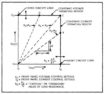
(ceiling) when the supply is used as a constant current source. The supply will automatically cross over from constant voltage to constant current operation and vice versa if the output current or voltage exceeds these preset limits.
1-3 The power supply contains an added feature for protection of delicate loads. A limit can be set on the output voltage. If this limit is exceeded the output will automatically be shorted.
1-4 The power supply has rear output terminals. Either the positive or negative output terminal may be grounded or the power supply can be operated floating at up to a maximum of 300 volts above ground.
1-5 Output voltage and current are continuously monitored on two front panel meters.
1-6 TerminaIs located at the rear of the unit allow access to various control points within the unit to expand the operating capabilities of the power supply. A brief description of these capabilities is given below:
a. Remote Programming. The power supply output voltage or current may be programmed (con- trolled) from a remote location by means of an external voltage source or resistarice.
b.Remote-Sensing. The degradation in regulation which occurs at the load due to voltage drop in the load leads can be reduced by using the power supply in the remote sensing mode of operation.
c.Auto-Series Operation. Power supplies
1-1
TM 11-6625-2958-14&P
may be used in series when a higher output voltage is required in the constant voltage mode of opera- t ion or when greater voltage compliance is required in the constant current mode of operation. AutoSeries operation permits one-knob control of the total output voltage from a “master” supply.
d. Auto-Parallel Operation. The power supply may be operated in parallel with a similar unit when greater output current capability is required.
Auto-Parallel operation permits one-knob control of the total output current from a “master” supply.
e. Auto-Tracking. The power supply may be used as a “master” supply controlling one or more “slave” supplies furnishing various voltages for a system.
1-7 SPECIFICATIONS
1-8 Detailed specifications for the power supply are given in Table 1-1 on Page 1-3.
1-9 OPTIONS
1-10 Options are customer-requested factory modifications of a standard instrument. The following options are available for the instrument covered by this manual. Where necessary, detailed coverage of the options is included throughout the manual.
Option No. |
Description |
005 50Hz Regulator Realignment: Standard instruments are designed for 57 to 63 Hz operation. Option 005 (factory realignment) is necessary when the instrument is to be operated from a 50Hz ac source. The option consists of changing a resistor in the preregu - lator circuit and adjusting the preregulator tracking.
007 Ten-Turn Output Voltage Control: A single control that replaces the coarse voltage control and allows
greater resolution in setting the output voltage.
008 Ten-Turn Output Current Control: A single control that replaces the coarse current control and allows
greater resolution in setting the output current.
009 Ten-Turn Output Voltage and Current Controls: Options 007 and 008 on the same instrument.
010 Chassis Slides: Enables convenient access to power supply interior for maintenance purposes.
013 Three Digit Graduated Decadial Voltage Control: A single control that replaces the coarse voltage control and allows accurate resetting of the output voltage.
Option |
No. |
|
Description |
|
014 |
Three Digit Graduated Decadial Cur- |
|||
|
rent Control: A single control that |
|||
|
replaces the coarse current control |
|||
|
and allows accurate resetting of the |
|||
|
output |
current. |
||
|
Rewire for 115Vac Input (6260B only): |
|||
|
Consists of replacing the input power |
|||
|
transformer and circuit breaker, and |
|||
|
reconnecting the bias transformer, RFI |
|||
|
choke, |
and fans for 115Vac operation. |
||
020 Voltage Programming Adjustment: Two rear panel mounted, screwdriveradjustable controls that allow accurately setting the zero volt output and the constant voltage programming coefficient.
021 Current Programming Adjustment: Two rear panel mounted, screwdriveradjustable controls that allow accurately setting the zero current output and the constant current programming coefficient.
022 Voltage and Current Programming Adjustments: Options 020 and 021 on the same instrument.
Rewire for 115Vac Input (6259B, 6261B, and 6268B only): Consists of replacing the line circuit breaker, and reconnecting the input power transformer, bias transformer, RF I choke, and fans for 115Vac operation.
027 Rewire for 208Vac Input: Consists of reconnecting the input power transformer and bias transformer for 208V ac operation.
1-11 lNSTRUMENT/MANUAL IDENTIFICATION
1-12 Hewlett-Packard power supplies are identified by a two-part serial number. The first part is the serial number prefix, a number-letter combination that denotes the date of a significant design change and the country of manufacture. The first two digits indicate the year (10= 1970, 11= 1971, etc.), the second two digits indicate the week, and the letter “A” designates the U.S.A. as the country of manufacture. The second part is the power supply serial
number; |
a different sequential number is assigned |
to each |
power supply, starting with 00101. |
1-13 If the serial number on your instrument does not agree with those on the title page of the manual, Change Sheets supplied with the manual or Manual Backdating Changes in Appendix A define the differences between your instrument and the instrument described by this manual.
1-2
1-14 ORDERING ADDITIONAL MANUALS |
|
|
|
|
|
TM 11-6625-2958-14&P |
||||
your local Hewlett-Packard field office (see list at |
||||||||||
1-15 One manual is shipped with each power sup- |
rear of this manual for addresses). Specify the |
|||||||||
model number, serial number prefix, and HP part |
||||||||||
ply. Additional manuals may be purchased from |
number shown on the title page. |
|
||||||||
|
Table 1-1. Specifications |
|
|
|
|
|
|
|||
|
|
|
|
|
|
|
|
|
|
|
INPUT: |
|
METERS: |
|
|
|
|
|
|
|
|
230Vac *10%, single phase, 57-63 Hz, 18A, |
A front panel voltmeter (0-50V) and ammeter |
|||||||||
2500W @ 230V. |
|
(0-60A) is provided. |
(Accurate within 2% of full |
|||||||
OUTPUT : |
|
scale. ) |
|
|
|
|
|
|
|
|
|
|
|
|
|
|
|
|
|
||
0-40 volts @ 0-50 amperes. |
OUTPUT CONTROLS: |
|
|
|
|
|||||
|
|
|
|
|
|
|||||
LOAD REGULATION: |
Single-turn |
coarse |
and |
fine |
voltage and current |
|||||
controls are |
included |
on |
the |
front panel. |
||||||
Constant Voltage - Less than 0.01% plus 200µV |
||||||||||
|
|
|
|
|
|
|
|
|||
for a load current change equal to the current |
OUTPUT TERMINALS: |
|
|
|
|
|||||
rating of the supply. |
|
|
|
|
||||||
Constant Current - Less than 0.02% plus 2mA |
Output bus bars are located on the rear of the |
|||||||||
for a load voltage change equal to the voltage |
chassis. Both bus bars are isolated from the |
|||||||||
rating of the supply. |
chassis and either the positive or negative bus |
|||||||||
|
|
bar may be connected to the chassis through a |
||||||||
LINE REGULATION : |
separate, |
adjacent |
ground terminal. |
|
||||||
Constant Voltage - Less than 0.01% plus 200µV |
REMOTE VOLTAGE PROGRAMMING: |
|
||||||||
for a change in line voltage from 207 to 253 volts |
|
|||||||||
All programming terminals are on a rear |
||||||||||
at any output voltage and current within rating. |
||||||||||
barrier strip. |
|
|
|
|
|
|
||||
Constant Current - Less than 0.02% plus 2mA |
|
|
1V/volt |
(accuracy: 1%). |
||||||
Constant |
Voltage |
- |
||||||||
for a change in line voltage from 207 to 253 volts |
||||||||||
Constant |
Current |
- 10mV/amp (Accuracy 10%). |
||||||||
at any output voltage and current within rating. |
||||||||||
|
|
|
|
|
|
|
|
|||
RIPPLE AND NOISE: |
REMOTE RESISTANCE PROGRAMMING: |
|||||||||
All programming terminals are on a rear |
||||||||||
Constant Voltage - Less than 1mV rms, 5mV |
||||||||||
barrier strip. |
|
|
|
|
|
|
||||
P-P (dc to 20MHz). |
|
|
|
|
|
|
||||
Constant |
Voltage |
-200 |
ohms/volt |
(Accuracy: |
||||||
Constant Current - Less than 25mA rms. |
1%). |
|
|
|
|
|
|
|
||
|
|
|
|
|
|
|
|
|
||
TEMPERATURE RATINGS: |
Constant |
Current |
-4 |
ohms/ampere |
(Accuracy |
|||||
10%). |
|
|
|
|
|
|
|
|||
Operating: O |
to 55°C. Storage: -40 to +75°C. |
|
|
|
|
|
|
|
||
|
|
|
|
|
|
|
|
|||
TEMPERATURE |
COEFFICIENT: |
OVERVOLTAGE PROTECTION CROWBAR: |
||||||||
The minimum crowbar trip setting above the |
||||||||||
Constant Voltage - Less than O .01% plus 200µV |
desired operating output voltage” to prevent false |
|||||||||
change in output per degree Centigrade change in |
crowbar tripping is 5% of output voltage setting |
|||||||||
ambient following 30 minutes warm-up. |
plus 2 volts. Range is 4 to 45Vdc. |
|
||||||||
Constant Current - Less than 0.01% plus 4mA |
|
|
|
|
|
|
|
|
||
change in output per degree Centigrade change in |
COOLING: |
|
|
|
|
|
|
|
||
ambient following 30 minutes warm-up. |
|
|
|
|
|
|
|
|||
Forced air cooling is employed. The supply has |
||||||||||
|
|
|||||||||
STABILITY : |
|
two cooling |
fans. |
|
|
|
|
|
||
|
|
|
|
|
|
|
|
|
||
Constant Voltage - Less than O .03% plus 2mV |
WEIGHT: |
|
|
|
|
|
|
|
||
total drift for 8 hours following 30 minutes warm- |
|
|
|
|
|
|
|
|||
up under constant ambient conditions. |
95 lbs. (43.0 kg.) |
net. |
120 lbs. |
(54.5 kg.) |
||||||
Constant Current- Less than 0.03% plus 10mA |
shipping. |
|
|
|
|
|
|
|
||
total drift for 8 hours following 30 minutes warm- |
SIZE: |
|
|
|
|
|
|
|
||
up under constant ambient conditions. |
|
|
|
|
|
|
|
|||
|
|
7.0“ (17.8cm) H x 17.511 (44.4cm) D x 19.0” |
||||||||
TRANSIENT RECOVERY TIME: |
(48, 3 cm) W. The unit can be mounted in a |
|||||||||
Less than 50µsec is required for output voltage |
standard 19” |
rack panel. |
|
|
|
|||||
recovery (in constant voltage operation) to within |
|
|
|
|
|
|
|
|
||
10mV of the nominal output voltage following a |
FINISH: |
|
|
|
|
|
|
|
||
S ampere change in output current. |
Light gray front panel with dark gray case. |
|||||||||
|
|
|
|
|
|
|
|
|
|
|
1-3
TM 11-6625-2958-14&P
SECTION II
INSTALLATION
2-1 INITIAL INSPECTION
2-2 Before shipment, this instrument was inspected and found to be free of mechanical and electrical defects. As soon as the instrument is unpacked, inspect for any damage that may have occurred in transit. Save all packing materials until the inspection is completed. If damage is found, file a claim with the carrier immediately. HewlettPackard Sales and Service office should be notified.
2-3 MECHANICAL CHECK
2-4 This check should confirm that there are no broken knobs or connectors, that the cabinet and panel surfaces are free of dents and scratches, and that the meters are not scratched or cracked.
2-5 |
ELECTRICAL CHECK |
|
2-6 |
The instrument should be checked against |
|
its |
electrical specifications. Section V includes |
Figure 2-1. Outline Diagram |
a n “in-cabinet” performance check to verify proper |
||
instrument operation. |
|
|
2-7 INSTALLATION DATA
2-8 The instrument is shipped ready for bench operation. It is necessary only to connect the instrument to a source of power and it is ready for
operation.
.
2-9 LOCATION
2-10 This instrument is fan cooled. Sufficient space should be allotted so that a free flow of cooling air can reach the sides of the instrument when it is in operation. It should be used in an area where the ambient temperature does not exceed 55°C.
2-11 OUTLINE DIAGRAM
2-12 Figure 2-1 illustrates the outline shape and dimensions of Models 6259B, 6260B, 6261B, 6268B, and 6269B.
2-13 RACK MOUNTING
2-14 This instrument is full rack size and can be easily rack mounted in a conventional 19 inch rack panel using standard mounting screws,
2-15 INPUT POWER REQUIREMENTS
2-16 Model 6259B, 6260B, 6261B, or 6268B power supply may be operated continuously from either a nominal 230 volt, 208 volt, or 115 volt 57-63Hz power source. Model 6269B may be operated from a 230 volt or 208 volt, 57-63Hz power source only. The instrument as shipped from the factory is wired for 230 volt operation. The input power when operated from a 230 volt power source at full load is:
Model |
Input Current |
Input Power |
6259B |
6A |
850W |
6260B |
12A |
1600W |
6261B |
11A |
1500W |
6268B |
11A |
1600W |
6269B |
18A |
2500W |
2-17 CONNECTIONS FOR 208 VOLT OPERATION (Model 6259B, 6261B, or 6268B: Option 027)
2-18 To convert Model 6259B, 6261B, or 6268B to operation from a 208Vac source, taps on the power and bias transformers must be changed as follows:
a. Remove RFI assembly as described in Steps (a) through (c) of Paragraph 5-67. Access is now provided to bias transformer A3T2. (See Figure 7-2.)
2-1
 6269b User Manual")
TM 11-6625-2958-14&P
Figure 2-2. Bias Transformer Primary Connections for 208Vac Operation (Model 6259B, 6260B, 6261B, 6268B, and 6269B) and 115Vac Operation
(Except Model 6269B)
b. Unsolder wire from circuit breaker A5CB1 connected to "230V" terminal of bias transformer A3T2 and solder it instead to "208V" terminal of
transformer (see Figure 2-2 B). Leave wire from fan B2 (not used in 62599) soldered to “230V” terminal.
c.Re-install RFI assembly by reversing procedure of Step (a).
d.Unsolder wire connected to terminal 5 of power transformer T1 (see Figure 7-4) and solder it instead to terminal 4 of transformer (see Figure
2-3 B).
Figure 2-3. Power Transformer Primary Connections for 208Vac and 115Vac Operation
. (Model 6259B, 6261B, and 6268B)
2-19 CONNECTIONS FOR 208 VOLT OPERATION (Model 6260B and 6269B: Option 027)
2-20 To convert Model 6260B or 6269B to operation from a 208Vac source, taps on the power and bias transformers must be changed as follows:
a. Perform Steps (a) through (c) of Paragraph
2-18.
b. Unsolder wire connected to to "230V” terminal
2-2
TM 11-6625-2958-14&P
Figure 2-4. Power Transformer T 1 Primary Connections for 208Vac Operation
(Model 6260B and 6269B)
of power transformer T1 (see Figure 7-4) and solder it instead to "208V" terminal of transformer (see Figure 2-4 B).
2-21 CONNECTIONS FOR 115 VOLT OPERATION (Model -6259B, 6261B, and 6268B: Option 026)
2-22 To convert Model 6259B, 6261B, or 6268B to operation from a 115Vac source, a new circuit breaker must be installed and taps must be changed on the bias transformer, power transformer, and RFI choke as follows:
a.Obtain and install new LINE circuit breaker (A5CB1). Connections to new circuit breaker are same as old connections. Refer to Option 026 in Table 6-4 (Replaceable Parts) for current rating and HP Part Number.
b.Remove and partially disassemble RFI
assembly as described in Steps (a) through (d) of Paragraph 5-67.
c.Unsolder jumper between terminals 2 and 3 of RFI choke mounting board and solder jumpers between terminals 1 and 3, 2 and 4 (see Figure 2-5 B). Replace cover on RFI assembly.
d.Unsolder wires from circuit breaker A5CB1 and fan B2 connected to "230V" terminal of bias transformer A3T2 (see Figure 7-2). Solder wire from circuit breaker to "115V" terminal of transformer, and solder wire from fan to "0V" terminal of transformer (see Figure 2-2 C). Note that
Figure 2-5. RFI Choke (A2L1A/A2L1B) Connections for 115Vac Operation (Model 6259B, 6260B, 6261B, and 6268B)
fan B2 is not used in Model 6259B.
e.Re-install RFI assembly by reversing procedure of Step (b).
f.Unsolder jumper connecting terminals 2 and 3 of power transformer T1 (see Figure 7-4) and solder jumpers between terminals 1 and 3, 2 and 5 (see Figure 2-3 C).
2-23 CONNECTIONS FOR 115 VOLT OPERATION
(Model 6260B: Option 016)
2-24 To convert Model 6260B to operation from a 115Vac source, a new power transformer and circuit breaker must be installed and taps must be changed on the RFI choke and bias transformer as follows:
a. Obtain and install new power transformer (T1) and new circuit breaker (A5CB1). Refer to Option 016 in Table 6-4 (Replaceable Parts) for power ratings and HP Part Numbers. New transformer has two primary terminals. Transfer wire from old transformer "0V" terminal to new transformer "0V" terminal, and wire from old transformer "230V" terminal to new transformer "115V" terminal. New circuit breaker connections are same as old.
2-3
TM 11-6625-2958-14&P
b. Perform Steps (b) through (e) of Paragraph
2-22.
2-25 CONNECTIONS FOR 50Hz OPERATION
2-26 For operation from a 50Hz ac input, R82 must be replaced with a 240 Ω, ±5%, ½ watt resistor as specified under Option 005 in Table 6-4 (Replaceable Parts). In addition, it is necessary to readjust the voltage drop across the series regula-
tor (“Preregulator Tracking” , Paragraph 5-103) and to check the ripple imbalance as described in Steps
(a) through (e) of Paragraph 5-101.
2-27 POWER CABLE
2-28 A power cable is not supplied with the instrument. It is recommended that the user-supplied power cable have three conductors (third conductor
grounded) and be of sufficient wire size to handle the input current drawn by the supply (see Paragraph 2-16). Note that when the supply is operated from a 115Vac source, the input current is approximately double that shown in Paragraph 2-16.
2-29 REPACKAGING FOR SHIPMENT
2-30 To insure safe shipment of the instrument, it is recommended that the package designed for the instrument be used. The original packaging material is reusable. If it is not available, contact your local Hewlett-Packard field office to obtain the materials. This office will also furnish the address of the nearest service center to which the instrument can be shipped. Be sure to attach a tag to the instrument specifying the owner, model number,
full serial number, and service required, or a brief description of the trouble.
2-4

TM 11-6625-2958-14&P
SECTION Ill
OPERATING INSTRUCTIONS
Figure 3-1. Front Panel Controls and Indicators,’ Modal 6259B, 6260B, 6261B, 6268B or 6269B
3-1 TURN-ON CHECKOUT PROCEDURE
3-2 The following checkout procedure describes the use of the front panal controls and indicators (Figure 3-1) and ensures that the supply is operational.
a.Set LINE circuit breaker to ON, and observe that pilot light lights.
b.Adjust VOLTAGE controls until desired
voltage |
is indicated |
on |
voltmeter . |
c. |
To ensure |
that |
overvoltage crowbar cir- |
cuit is operational, rotate OVERVOLTAGE ADJUST control (screwdriver adjust) counterclockwise until unit crowbars. Overvoltage lamp will light and output voltage will fall to zero volts.
d. To deactivate crowbar, return OVERVOLTAGE ADJUST control to its maximum clockwise position and turn off supply. Turn supply back on and voltage should again be value obtained in step
(b).
e. To check out constant current circuit, turn off supply. Short circuit rear output terminals and turn on supply.
f.Adjust CURRENT controls until desired output current is indicated on ammeter .
g.Remove short circuit and read following paragraphs before connecting actual load to supply.
3-3 OPERATING MODES
3-4 The power supply is designed so that its mode of operation can be selected by making strapping connections between particular terminals on the terminal strip at the rear of the power supply. The terminal designations are stenciled in white on the power supply below their respective terminals. The following paragraphs describe the procedures for utilizing the various operational capabilities of the power supply. A more theoretical description concerning the operational features of this supply is contained in Application Note 90, Power Supply Handbook (available at no charge from your local Hewlett-Packard sales office). Sales office addresses appear at the rear of the manual.
3-5 NORMAL OPERATING MODE
3-6 The power supply is normally shipped with its rear terminal strapping connections arranged for constant voltage/constant current, local sensing, local programming, single unit mode of operation. This strapping pattern is illustrated In Figure 3-2. The operator selects either a constant voltage or a constant current output using the front panel controls (local programming; no strapping changes are necessary).
3-1

TM 11-6625-2958-14&P
|
Figure 3-2. Normal Strapping Pattern |
3-7 |
CONSTANT VOLTAGE |
3-8 |
To select a constant voltage output, proceed |
as |
follows: |
a.Turn on power supply and adjust VOLTAGE controls for desired output voltage with output terminals open.
b.Short circuit output terminals and adjust CURRENT controls for maximum output current allowable (current limit), as determined by load con-
ditions. |
If a load |
change causes the current limit |
to be |
exceeded, |
the power supply will automatical- |
ly cross over to constant current output at the preset current limit and the output voltage will drop proportionately. In setting the current Iimit, allowance must be made for high peak currents which
can cause unwanted crossover. (Refer to Paragraph 3-60. )
3-9 CONSTANT CURRENT
3-10 To select a constant current output, proceed as follows:
a.Short circuit output terminals and adjust CURRENT controls for desired output current.
b.Open output terminals and adjust VOLTAGE controls for maximum output voltage allowable
(voltage limit ), as determined by load conditions. If a load change causes the voltage limit to be exceeded, the power supply will automatically cross over to constant voltage output at the preset voltage limit and the output current will drop proportionately. In setting the voltage limit, allowance must be made for high peak voltages which can cause unwanted crossover. (Refer to Paragraph 3-60.)
3-11 OVERVOLTAGE TRIP POINT ADJUSTMENT
3-12 The crowbar trip voltage can be adjusted by using the screwdriver control on the front panel. The trip voltage range is as follows:
6259B, 6260B |
6 2 6 1 B |
6268B, 6269B |
2 to 12Vdc |
2 to 23Vdc |
4 to 45Vdc |
When the crowbar trips, the output is shorted and the amber indicator on the front panel lights.
Clockwise rotation of the control produces higher trip voltages. The factory sets the control fully clockwise. The crowbar may be disabled completely if desired. (Refer to Paragraph 5-11 1.)
3-13 False crowbar tripping must be considered when adjusting the trip point. If the trip voltage is set too close to the operating output voltage of the supply, a transient in the output will falsely trip the crowbar. It is recommended that the crowbar be set higher than the output voltage by 5% of the output voltage plus 2 volts. However, If occasional crowbar tripping on unloading can be tolerated, the crowbar trip point can be set much closer to the operating out put voltage of the supply.
3-14 CONNECTING LOAD
3-15 Each load should be connected to the power supply output terminals using separate pairs of connecting wires. This will minimize mutual coupling effects between loads and will retain full advantage of the low output impedance of the power supply. Each pair of connecting wires should be as short as possible and twisted or shielded to reduce noise pickup. (If a shielded pair is used, connect one end of the shield to ground at the power supply and leave the other end unconnected.)
3-16 If load considerations require that the output power distribution terminals be remotely located from the power supply, then the power suppIy output terminals should be connected to the remote distribution terminals via a pair of twisted or shielded wires and each load should be separately connected to the remote distribution terminals. For this case, remote sensing should be used. (Refer to Paragraph 3-4 1.)
3-17 Positive or negative voltages can be obtained from this supply by grounding either one of. the output terminals or one end of the load. Always use two leads to connect the load to the supply, regardless of where the setup is grounded. This will eliminate any possibility of output current return paths through the power source ground which would damage the line cord plug. This supply can also be operated up to 300Vdc above ground, if neither output terminal is grounded.
3-18 NO LOAD OPERATION
3-19 When the supply is operated without a load, down-programming speed is considerably slower than in normal loaded operation. This slower programming speed is evident when using any method of down-programming - either turning the VOLTAGE controls fully counterclockwise, activating the crowbar, or throwing the LINE circuit breaker to OFF. Under any of these conditions, the supply output will rapidly fall to approximately two volts,
3-2

then proceed at a slower rate towards zero. The actual time required for the output to fall from two volts to zero will vary from several seconds to several minutes, depending upon which down-pro- gramming method is used.
3-20 OPERATION BEYOND RATED OUTPUT
3-21 The shaded area on the front panel meter face indicates the approximate amount of output voltage or current that may be available in excess of the normal rated output. Although the supply can be operated in this shaded region without being damaged, it cannot be guaranteed to meet all of its performance specifications.
3-22 OPTIONAL OPERATING MODES
3-23 REMOTE PROGRAMMING, CONSTANT VOLTAGE
3-24 The constant voltage output of the power supply can be programmed (controlled) from a remote location if required. Either a resistance or voltage source can be used as the programming device. The wires connecting the programming terminals of the supply to the remote programming device should be twisted or shielded to reduce noise pickup. The VOLTAGE controls on the front panel are automatically disabled in the following procedures.
3-25 Resistance Programming (Figure 3-3). In this mode, the output voltage will vary at a rate determined by the voltage programming coefficient of 200 ohms/volt. The programming coefficient is determined by the programming current. This current is factory adjusted to within 1% of 5mA. If greater programming accuracy is required, it may be achieved by either adjusting R3 as discussed in Paragraph 5-88, or, if the instrument is equipped with Option 020, by adjusting potentiometer R112 as discussed in Paragraph 5-89.
Figure 3-3. Remet e Resistance Programming
(Constant Voltage)
TM 11-6625-2958-14&P 3-26 The output voltage of the supply should be
-15mV ±5mV when zero ohms is connected across the programming terminals. If a zero ohm voltage closer to zero than this is required, it may be achieved by inserting and adjusting R110 as discussed in Paragraph 5-83, or, if the instrument is equipped with Option 020, by adjusting potentiometer R113 as discussed in Paragraph 5-85.
3-27 To maintain the stability and temperature coefficient of the power supply, use programming resistors that have stable, low noise, and low temperature coefficient (less than 30ppm per degree Centigrade) characteristics. A switch can be used in conjunction with various resistance values in order to obtain discrete output voltages. The switch should have make-before-break contacts to avoid momentarily opening the programming terminals during the switching interval.
Figure 3-4. Remet e Voltage Programming,
Unity Gain (Constant Voltage)
3-28 Voltage Programming, Unity Gain (Figure 3-4). Employ the strapping pattern shown in Figure 3-4 for voltage programming with unity gain. In this mode, the output voltage will vary in a 1 to 1 ratio with the programming voltage (reference voltage) and the load on the programming voltage source will not exceed 20 microampere. Impedance matching
resistor (Rx) is |
required |
to maintain the |
temperature |
coefficient and |
stability |
specifications |
of the sup- |
ply . |
|
|
|
3-29 Voltage Programming, Non-Unity Gain (Figure 3-5). The strapping pattern shown in Figure 3-5 can be utilized for programming the power supply using an external voltage source with a variable voltage gain. The output voltage in this configuration is found by multiplying the external voltage source by (Rp/RR).
3-30 |
External resistors Rp and RR should have sta- |
ble, |
low noise, and low temperature coefficient |
3-3
TM 11-6625-2958-14&P
Figure 3-5. Remote Voltage Programming,
Non-Unity Gain (Constant Voltage)
(less than 30ppm Per degree Centigrade) characteristics in order to maintain the Supply's temperature and stability specifications. Reference resistor RR should not exceed 10K. Note that it is possible to use the front panel voltage control already in the supply (A5R121) as the voltage gain control (Rp) by simply removing the external Rp and strapping terminals Al and A2 together.
3-31 The output voltage of the supply may be adjusted to exactly zero when the external programming voltage is zero by either inserting and adjusting R111 as discussed in Paragraph 5-84, or, if the instrument is equipped with Option 020, by adjusting potentiometer R112 as discussed in Paragraph 5-86.
3-32 REMOTE PROGRAMMING, CONSTANT CURRENT
3-33 Either a resistance or a voltage source can be used to control the constant current output of the supply. The CURRENT controls on the front panel are automatically disabled in the following procedures.
3-34 Resistance Programming (Figure 3-6). In this mode, the output current varies at a rate determined
by the programming |
coefficient as |
follows: |
Model |
Programming |
Coefficient |
6259B |
4 ohms/ampere |
|
6260B |
2 ohms/ampere |
|
6261B |
4 ohms/ampere |
|
6268B |
6 ohms/ampere |
|
6269B |
4 ohms/ampere |
|
The programming coefficient is determined by the constant current programming current which is adjusted to within 10% of 2.5mA at the factory. If greater programming accuracy is required, it may be achieved by either adjusting R30 as discussed
in Paragraph 5-97, or, if the instrument is equipped
Figure 3-6. Remote Resistance Programming
(Constant Current)
with Option 021, by adjusting potentiometer R116 as discussed in Paragraph 5-98. The output current of the supply when zero ohms is placed across the programming terminals may be set to exactly zero by either inserting and adjusting R117 as discussed in Paragraph 5-92, or, if the instrument is equipped with Option 021, by adjusting potentiometer R119 as discussed in Paragraph 5-94.
3-35 Use stable, low noise, low temperature coefficient (less than 30ppm/°C) programming resistors to maintain the power supply temperature coefficient and stability s pacifications. A switch may be used to set discrete values of output current. A make-before-break type of switch should be used since the output current will exceed the maximum rating of the power supply if the switch contacts open during the switching interval.
C A U T I O N
If the programming terminals (A4 and A 6) should open at any time during the remote resistance programming mode, the output current will rise to a value that may damage the power supply and/or the load. If, in the particular programming configuration in use, there is a chance that the terminals might become open, it is suggested that a 200 ohm resistor be connected across the programming terminals. Like the programming resistor, this resistor should be a low noise, low temperature coefficient type. Not e that when this resistor is used, the resistance value actually programming the supply is the parallel combination of the remote programming resistance and the resistor across the programming terminals.
3-4

Figure 3-7. Remote Voltage Programming,
Unity Gain (Constant Current]
3-36 Voltage Programming , Unity Gain (Figure 3-7). In this mode, the output current will vary linearly with changes in the programming voltage. The programming voltage should not exceed 0.6 volts.
Voltage in excess of 0.6 |
volts will result in exces- |
sive power dissipation in |
the instrument and possi- |
ble damage. |
|
3-37 The output current varies at a rate determined by the programming coefficient as follows:
Model |
Programming Coefficient |
6259B |
10.0mV/ampere |
6260B |
5.0mV/ampere |
6261B |
10.0mV/ampere |
6268B |
16.7mV/ampere |
6269B |
10.0mV/ampere |
The current required from the voltage source will be less than 20µA. Impedance matching resistor Rx is required to maintain the temperature coefficient and stability specifications of the supply.
3-38 Voltage Programming, Non-Unity Gain (Figure 3-8). The power supply output current can be
TM 11-6625-2958-14&P programmed using an external voltage source with variable gain by utilizing the strapping pattern shown in Figure 3-8. In this mode, the output current is found by multiplying the external voltage source (Es) by [Rp/(RR x Kp)], where Kp is the constant current voltage programming coefficient as given in Paragraph 3-37. The value of reference
resistor |
RR and |
programming voltage source Es |
|
|
should |
be such |
that the value of ES/RR is |
equal |
to |
or greater than 2.5mA. |
|
|
||
3-39 External resistors Rp and RR should |
have |
sta- |
||
ble, low noise, |
and low temperature coefficient |
|
||
(less than 30ppm per degree Centigrade) characteristics in order to maintain the stability and temperature specifications of the Power supply. Reference resistor RR should not exceed 10K. Note that it is possible to use the front panel current control already in the supply (A5R123) as the gain control (Rp) by simply removing the external Rp and strapping terminals AS and A6 together.
3-40 The output current of the supply may be adjusted to exactly zero when the external programming voltage is zero by either inserting and adjusting R115 as discussed in Paragraph 5-93, or, if the instrument is equipped with Option 021, by adjusting potentiometer R116 as discussed in Paragraph 5-95.
3-41 REMOTE SENSING (Figure 3-9)
3-42 Remote sensing is used to maintain good regulation at the load and reduce the degradation of regulation which would occur due to the voltage drop in the leads between the power supply and the load. Remote sensing is accomplished by utilizing the strapping pattern shown in Figure 3-9. The Power supply should be turned off before changing strapping paterns. The leads from the sensing (±S) terminals to the load will carry much less current than the load leads and it is not required that these leads be as heavy as the load leads. However, they must be twisted or shielded to minimize noise pickup.
Figure 3-8. Remote Voltage Programming, |
|
Non-Unity Gain (Constant Current) |
Figure 3-9. Remote Sensing |
3-5

TM 11-6625-2958-14&P
3-43 For reasonable load lead lengths, remote sensing greatly improves the performance of the supply. However, if the load is located a considerable distance from the supply, added precautions must be observed to obtain satisfactory operation. Notice that the voltage drop in the load leads subtracts directly from the available output voltage and also reduces the amplitude of the feedback error signals that are deveIoped within the unit. Because of these factors it is recommended that the drop in each load lead not exceed 0.5 volt. If a larger drop must be tolerated, please consult an HP Sales Engineer.
NOTE
Due to the voltage drop in the load leads, it may be necessary to readjust the current limit in the remote sensing mode.
3-44 Observance of the precautions in Paragraph 3-43 will result in a low dc output impedance at the load. However, another factor that must be considered is the inductance of long load leads. This causes a high ac Impedance and could affect the stability of the feedback loop seriously enough to cause oscillation. If this is the case, it is recommended that the following actions be taken:
a.Adjust equalization control R47 to remove oscillation, or to achieve best possible transient response for given long load lead configuration. Refer to Paragraph 5-27 for discussion of transient response measurement.
b.If performing adjustment in step (a) above does not remove oscillation, disconnect output capacitor A3C3 and connect a capacitor having similar characteristics (approximately the same capacitance, the same voltage rating or greater, and
having good high frequency characteristics) directly across load using short leads. Readjust equalization control R47 as in step (a) above after making this change. In order to gain access to capacitor A3C3, it is necessary to remove the RFI assembly as described in steps (a) through (c) of Paragraph 5-67. Lead from positive side of capacitor (shown arrowed In Figure 7-2) can then be unsoldered from A3 interconnection circuit board.
3-45 To employ remote sensing with any method of remote programming or with any method of combining more than one supply discussed in the Preceding or following paragraphs, use the following procedure:
a. Remove the two external leads connecting the sensing terminals (±S) to the output bus bars (±OUT).
b. Connect a lead from the +S terminal to the positive side of the load, and connect another lead
from the -S terminal to the negative side of the load. Note that there may be more than one lead connected to the +S and -S terminals.
3-46 AUTO-PARALLEL OPERATION (Figure 3-10)
3-47 Two or more power supplies can be connected in an Auto-Parallel arrangement to obtain an output
Figure 3-10. Auto-Parallel Operation,
Two and Three Units
3-6
current greater than that available from one supply. Auto-Parallel operation permits equal current sharing under all load conditions, and allows complete control of the output current from one master power supply. The output current of each slave will be approximately equal to the master’s output current regardless of the load conditions. Because the output current controls of each slave are operative, they should be set to maximum to prevent the slave reverting to constant current operation; this would OCCur if the master output current setting exceeded the slave’s.
3-48 Additional slave supplies may be added in parallel with the master/slave combination as shown in the bottom half of Figure 3-10. All the connections between the master and slave #1 are duplicated between slave #1 and the added slave supply. In addition, the strapping pattern of the added slave should be the same as slave #1. Remote sensing and programming can be used, though the strapping arrangements shown in Figure 3-10 show local sensing and programming.
3-49 Overvoltage protection is controlled by the crowbar circuit in the master supply which monitors the voltage acress the load and fires the SCR's in both units if an overvoltage condition occurs. The firing pulses are fed to the slave supply from transformer T90 (winding 5-6) of the master supply
"
through the “ EXT. CROWBAR TRIGGERterminals on the rear panel of the master supply. Correct polarity must be observed in connecting the crowbars together. The overvoltage trip point is adjusted on the master supply, The OVERVOLTAGE ADJUST potentiometer on the slave supply should be set to maximum [clockwise) so that the master crowbar will control the slave.
3-50 AUTO-SERIES OPERATION (Figure 3-11)
3-51 Two or more power supplies can be operated in Auto-Series to obtain a higher voltage than that available from a single supply. When this connection is used, the output voltage of each slave supply varies in accordance with that of the master supply. At maximum output voltage, the voltage of the slaves is determined by the setting of the front panel VOLTAGE controls on the master. The master supply must be the most positive supply of the series. The output CURRENT controls of all series units are operative and the current limit is equal to the lowest control setting. If any of the output CURRENT controls are set too low, automatic crossover to constant current operation will occur and the output voltage will drop. Remote sensing and programming can be used, though the strapping ar-
rangements shown in Figure 3-11 show local sensing and programming.
3-52 In order to maintain the temperature coeffi-
TM 11-6625-2958-14&P
Figure 3-11. Auto-Series Operation,
Two and Three Units |
|
cient and stability specifications of the |
power sup- |
ply, the external resistors (Rx) shown in |
Figure |
3-11 should be stable, low noise, low temperature coefficient (less than 30ppm per degree Centigrade) resistors. The value of each resistor is dependent
3-7

TM 11-6625-2958-14&P
on the maximum voltage rating of the "master" supply. The value of RX is this voltage divided by the voltage programming current of the slave supply (1/Kp where KP is the voltage programming coefficient). The voltage contribution of the slave is determined by its voltage control setting.
3-53 Overvoltage protection is provided in AutoSeries operation by connecting the crowbars in parallel with correct polarity as in Auto-Parallel operation (see Paragraph 3-49). The OVERVOLTAGE ADJUST potentiometer in each supply should be adjusted so that it trips at a point slightly above the output voltage that the supply will contribute.
3-54 When the center tap of an Auto-Series combination is grounded, coordinated positive and negative voltages result. This technique is commonly referred to as “robber-banding” and an external reference source may be employed if desired. Any change of the internal or external reference source (e.9. drift, ripple) will cause an equal percentage change in the outputs of both the master and slave supplies. This feature can be of considerable use in analog computer and other applications, where the load requires a positive and a negative power supply and is less susceptible to an output voltage change occurring simultaneously in both supplies than to a change in either supply alone.
3-55 AUTO-TRACKING OPERATION (Figure 3-12)
3-56 The Auto-Tracking configuration is used when several different voltages referred to a common bus must vary in proportion to the setting of a particular instrument (the control or master). A fraction of the master’s output voltage is fed to the comparison amplifier of the slave supply, thus controlling the slave's output. The master must have the largest output voltage of any power supply in the group. It must be the most positive supply in the example shown on Figure 3-12.
3-57 The output voltage of the slave (Es) is a percentage of the master's output voltage (EM), and is determined by the voltage divider consisting of RX and the voltage control of the slave supply, Rp, where ES = EM [Rp/(Rx+Rp)]. Remote sensing and programming can be used (each supply senses at its own load), though the strapping patterns given in Figure 3-12 show only local sensing and programming. In order to maintain the temperature coefficient and stability specifications of the power supply, the external resistors should be stable, low noise, low temperature coefficient (less than 30ppm per degree Centigrade) resistors.
3-58 The overvoltage protection circuit in each unit is operable end independently monitors the voltage across its own load. Notice that if the master supply crowbars, the output voltage of
Figure 3-12. Auto-Tracking, TwO and Three Units
each slave will also decrease. However, the reverse is not true. If one of the slave units crowbars, the other supplies in *the ensemble will not be affected.
3-59 SPECIAL OPERATING CONSIDERATIONS
3-60 “PULSE LOADING
3-61 The power supply will automatically cross
3-8
over from constant voltage to constant current operation, or the reverse, in response to an increase (over the preset limit) in the output current or voltage, respectively. Although the preset limit may be set higher than the average output current or voltage, high peak currents or voltages (as occur in pulse loading) may exceed the preset limit and cause crossover to occur. If this crossover limiting is not desired, set the preset limit for the peak requirement and not the average.
3-62 OUTPUT CAPACITANCE
3-63 An internal capacitor (A3C3) connected across the output terminals of the power supply, helps to supply high-current pulses of short duration during constant voltage operation. Any capacitance added externally will improve the P UlSe current capability, but will decrease the safety provided by the constant current circuit. A high-current pulse may damage load components before the average output current is large enough to cause the constant current circuit to operate.
3-64 The effects of the output capacitor during constant current operation are as follows:
a. The output impedance of the power supply decreases with increasing frequency.
b. The recovery time of the output voltage is longer for load resistance changes.
TM 11-6625-2958-14&P
c. A large surge current causing a high power dissipation in the load occurs when the load resistance is reduced rapidly.
3-65 REVERSE VOLTAGE LOADING
3-66 A diode (A4CR106) is connected across the
output |
terminals. |
Under normal operation condi- |
|
tions, |
the |
diode is |
reverse biased (anode connect- |
ed to |
the |
negative |
terminal). If a reverse voltage |
is applied to the output terminals (POSitive voltage applied to the negative terminal), the diode will conduct, shunting current across the output terminals and limiting the voltage across the output terminals to the forward voltage drop of the diode. This diode protects the series transistors and the output electrolytic capacitors.
3-67 REVERSE CURRENT LOADING
3-68 Active loads connected to the power supply may actually deliver a reverse current to the power supply during a portion of its operating cycle. An external source cannot be allowed to pump current into the supply without loss of regulation and possible damage to the output capacitor. To avoid these effects, it is necessary to preload the supply with a dummy load resistor so that the power supply delivers current through the entire operation cycle of the load device.
3-9
TM 11-6625-2958-14&P
SECTION IV
PRINCIPLES OF OPERATION
Figure 4-1. Overall Block Diagram
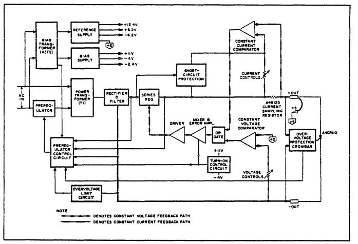
4-1 OVERALL BLOCK DIAGRAM DISCUSSION
4-2 The major circuits of the power supply are shown on the overall block diagram of Figure 4-1. The ac input voltage is first applied to the preregulator triac which operates in conjunction with the preregulator control circuit to form a feedback loop. This feedback loop minimizes the power dissipated by the series regulator by keeping the voltage drop across the regulator at a low and constant level.
4-3 To accomplish this, the preregulator control circuit issues a phase adjusted firing pulse to the triac once during each half cycle of the input ac.
The control circuit continuously samples the output voltage, the input line voltage (from A3T2), and the voltage across the series regulator and, on the
basis of these inputs, determines at what time each firing pulse is generated.
4-4 The phase adjusted output of the triac is applied to the power transformer where it is steppeddown and coupled to a full-wave rectifier and filter. The preregulated dc current is applied next to the series reguIator which varies its conduction to provide a regulated voltage or current at the output terminals.
4-5 The series regulator is part of another feedback loop consisting of the error and driver amplifiers and the constant voltage/constant current compactors. The series regulator feedback loop provides rapid, low magnitude regulation of the output while the preregulator feedback loop handles large, relatively slow, regulation demands.
4-1
TM 11-6625-2958-14&P
4-6 The feedback signals controlling the conduction of the series regulator originate within the constant voltage or constant current comparator. During constant voltage operation the constant voltage comparator continuously compares the output voltage of the supply with the drop across the VOLTAGE controls. If these voltages are not equal, the comparator produces an amplified error signal which is further amplified by the error amplifier and then fed back to the series regulator in the correct phase and amplitude to counteract the difference.
In this manner, the constant voltage comparator helps to maintain a constant output voltage and also generates the error signals necessary to set the output voltage at the level established by the VOLTA GE controls.
4-7 During constant current operation, the constant current comparator detects any difference between the voltage drop developed by the load current flowing through the current sampling resistor and the voltage acress the CURRENT controls. If the two inputs to the comparator are momentarily unequal, an error signal is generated which (after amplification) alters the conduction of the series regulator by the amount necessary to reduce the error voltage at the comparator input to zero. Hence, the IR drop across the current sampling resistor, and therefore the output current, is maintained at a constant value.
4-8 Since the constant voltage comparator tends to achieve zero output impedance and alters the output current whenever the load resistance changes, while the constant current comparator causes the output impedance to be infinite and changes the output voltage in response to any load resistance change, it is obvious that the two comparison amplifiers cannot operate simultaneously. For any-given value of load resistance, the power supply must act either as a constant voltage source or as a constant current source - it cannot be both.
4-9 Figure 4-2 shows the output characteristic of a constant voltage/constant current power supply. With no load attached (RL = ∞), IOUT = O, and
EOUT = Es, the front panel voltage control setting. When a load resistance is applied to the output terminals of the power supply, the output current increases, while the output voltage remains constant; point D thus represents a typical constant voltage operating point. Further decreases in load resistance are accompanied by further increases in IOUT with no change in the output voltage until the output current reaches Is, a value equal to the front panel current control setting. At this point the supply automatically changes its mode of operation and becomes a constant current source; still further decreases in the value of load resistance are accompanied by a drop in the supply output voltage with no accompanying change in the output current
Figure 4-2. Operating Locus of a CV/CC
Power Supply
value. With a short circuit across the output load terminals, IOUT = ES and EOUT = O.
4-10 The ‘: Crossover” value of load resistance can be defined as RC = Es/Is. Adjustment of the front panel voltage and current controls permits this
“crossover” |
resistance RC to be set to any desired |
|||
value from |
0 |
to ∞. If RL is greater than |
RC , the |
|
supply |
is |
in |
constant voltage operation, |
while if RL |
is less |
than RC , the supply is in constant current |
|||
operation. |
|
|
|
|
4-11 The short circuit protection circuit (see Fig- ure 4-1) protects the series regulator in the event of a shorted output when the controls are set to a high output voltage and current. The protection circuit monitors the voltage drop across the series regulator. If the drop rises above a preset level, the protection circuit limits the current through the series regulator until the preregulator can reduce the voltage across the series regulator. Once this voltage returns to normal, the short circuit protec-
tion circuit is |
turned off and has no effect on norm- |
al operation |
of the supply. |
4-12 The overvoltage protect ion crowbar monitors the output of the supply, and if it exceeds a preset (adjustable) threshold, fires an SCR which short circuits the supply. The circuit also sends a turndown signal to the preregulator control circuit.
4-13 The overvoltage limit circuit protects the main rectifier diodes and filter capacitors from damage that might occur if the series regulator transistors were shorted or the voltage programming pot were opened. The circuit monitors the output voltage of
4-2

the supply and, if it exceeds approximately 120% of maximum rated output, sends a turn-down signal
to the preregulator control circuit. |
Hence, the out- |
put voltage of the supply is limited |
to a “safe” val- |
ue despite any possible failure in the series regu- |
|
lator feedback loop. |
|
4-14 The turn-on control circuit is a long time constant network which allows the supply to achieve a gradual turn-on characteristic. The slow turn-on feature protects the preregulator triac and the series regulator from damage which might occur when ac power is first applied to the unit. At turnon, the control circuit sends inhibiting voltages to the preregulator control circuit and the s cries regulator (via the error and driver amplifiers). A short time after the unit is in operation, the inhibiting voltages are removed and the circuit no longer exercises any control over the operation of the supply.
4-15 The reference supply provides stable reference voltages used by the constant voltage and current comparators. Less critical operating voltages are obtained from the bias supply.
4-16 DETAILED CIRCUIT ANALYSIS (See
Figure 7-11)
4-17 PREREGULATOR CONTROL CIRCUIT
4-18 The preregulator minimizes changes in the power dissipated by the series regulating transis - tors due to output voltage or. input line voltage variations. Preregulation is accomplished by means of a phase control circuit utilizing triac A2CR1 as the switching element.
4-19 In order to understand the operation of the preregulator, it is important to understand the operation of the triac. The triac is a hi-directional device, that is, it can conduct current in either direction. Hence, the device fires whenever it receives a gating pulse regardless of the polarity of the input a c that is applied to it. The triac is fired once during each half-cycle (8.3 3 milliseconds) of the input ac (see Figure 4-3). Notice that when the triac is fired at an early point during the half-cycle, the ac level applied to the power transformer is relatively high. When the triac is fired later during the half-cycle, the ac level is relatively low.
4-20 Normally the ac input signal must be at a certain minimum potential before the triac will conduct. However, A2R1 and A2C1 provide a holding current that allows the triac to conduct at any time during the ac input cycle. RFI choke A2L1A/A2L1B (in series with the triac) slows down the turn-on of the triac in order to minimize spikes at the output of the supply. Components A2CR1, A2R1, A2L1A/ A2L1B, and A2C1 are all mounted inside a shielded
T M 1 1 - 6 6 2 5 - 2 9 5 8 - 1 4 & P
Figure 4-3. Triac Phase Control Over
AC Input Amplitude
box (assembly A2) to minimize radiated and reflected RFI. Further RFI suppression is provided by bypass capacitors C110 and C111.
4-21 The preregulator control circuit samples the input line voltage, the output voltage, and the voltage across the series regulator transistors. It generates firing pulses, at the time required, to fire the triac. This action maintains the ac input voltage across the primary winding of T I at the desired level.
4-22 The inputs to the control circuit are algebraically summed across capacitor C70. All inputs contribute to the time required to charge C70. The input line voltage is rectified by CR81, CR82, CR83, and CR84, attenuated by voltage divider R86 and R83, and applied to the summing point at the col - lector of Q71 (TP81) via capacitor C70. Capacitor C73 is used for smoothing purposes.
4-23 Transistor Q71, connected in a common base configuration, provides a charging current for the summing capacitor varying in accordance with the input signals applied to its emitter. Resistor R78, connected between the negative output line and the emitter of Q71, furnishes a signal which is propor- tional to the output voltage. Resistors R75 and R76 sample the voltage across, and the current through, the series regulator. Capacitor C72 and resistor R82 stabilize the entire preregulator feedback loop. Resistors R70 and R80 are the source of a constant offset current which sustains a net negative charg-
4-3

TM 11-6625-2958-14&P
ing current to the summing point, ensuring that the triac will fire at low output “voltages.
4-24 The summation of the input signals results in the generation of a voltage waveform at TP80
similar to that shown in waveform (A) of Figure 4-4. When the linear ramp portion of the waveform reaches a certain negative threshold voltage, diodes CR74 and CR75 become forward biased. The negative voltage is then coupled to the base of transistor Q72. Transistors Q72 and Q73 form a squaring circuit resembling a Schmitt trigger configuration. Q72 is conducting prior to firing time due to the positive bias connected to its base through R84, Transistor Q73 is cut off at this time because its base is driven negative by the collector of Q72.
4-25 When the negative threshold voltage is reached, transistor Q72 is turned off and Q73 is turned on. The conduction of Q73 allows capacitor C71 to discharge rapidly through pulse transformer T70 resulting in the generation of a firing pulse across the secondary winding of T70. As shown in
Figure 4-4. Preregulator Control Circuit Waveforms
waveform (C) of Figure 4-4, the firing pulse is quite narrow because Q73 saturates rapidly, causing the magnetic field surrounding T70 to collapse. Diode CR76 damps out positive overshoot.
4-26 Reset of the control circuit occurs once every 8.33 milliseconds when the rectified ac voltage at the junction of CR77, CR78, and CR79 (TP82) increases to a level at which diode CR78 becomes forward biased. Summing capacitor C70 is then allowed to discharge through CR78. Diodes CR74 and CR75 become reverse biased at reset and transistor Q72 reverts to its “on” state. Consequently, Q73 is turned off and capacitor C71 charges up through R79 at a comparatively slow rate until the collector voltage of Q73 reaches approximately +11 volts. The above action causes the small positive spike that appears across the windings of pulse transformer at T70 at reset time.
4-27 SERIES REGULATOR AND DRIVER
4-28 The series regulator consists of transistors A4Q103 through A4Q108 connected in parallel. The transistors serve as the series or “pass” element which provides precise and rapid control of the output. Resistors A4R150 through A4R155 allow high output currents to be equally shared by the series regulator transistors. The conduction of the series transistors is controlled by signals obtained from driver A4Q102, which is connected in a Darlington configuration with the parallel-connected series regulator transistors. Thermal switch A4TS101 opens if the heat sink assembly temperature exceeds approximately 230°F, thus turning off the series regulator transistors. This feature protects critical components of the supply from excessive temperatures which could occur if cooling fan A4B1 failed. Diode CR50 provides a discharge path for the output capacitors when the supply is rapidly downprogrammed; R57 limits the discharge current flowing through the diode and through error amplifier A4Q101. Diode A4CR105, connected across the regulator circuit, protects the series elements from reverse voltages that could develop across them during parallel operation if one supply is turned on before the other.
4-29 SHORT CIRCUIT PROTECTION
4-30 This circuit acts to initially protect the series regulator against a simultaneous full-voltage, fullcurrent conditions such as might occur if the output were shorted when the controls were set to deliver a high output voltage and current. Under this condition, Q20 goes into heavy conduction due to the increased voltage across the series regulator, putting R26 in parallel with the current controls and thus limiting the current to less than 10% of the supply’s rating. Within 10 milliseconds after the short circuit is imposed, the preregulator shuts off.
4-4
The input capacitor then begins to discharge through the series regulator, and the voltage across the regulator decreases until Q20 turns off. The discharge time (typically ½ to 4 seconds) depends on the voltage and current ratings of the supply, the main filter capacitor, and the control settings. Once this recovery time has elapsed, the output current will return to the level set by the current controls, and the preregulator will return the voltage across the series regulator to the normal 3.5V level, thus limiting the power dissipated by the
s cries regulator.
4-31 CONSTANT VOLTAGE COMPARATOR
4-32 This circuit consists of the programming resistors (A5R121 and A5R122) and a differential amplifier stage (Z1 and associated components). An integrated circuit is used for the differential amplifier to minimize differential voltages due to mismatched transistors and thermal differentials.
4-33 The constant voltage comparator continuously compares the voltage drop across the VOLTAGE controls with the output voltage and, if a difference exists, produces an error voltage whose amplitude is proportional to this difference. The error signal ultimately alters the conduction of the series regulator which, in turn, alters the output current so that the output voltage becomes equal to the voltage drop across the VOLTAGE controls. Hence, through feedback action, the difference between the two inputs to Z1 is held at zero volts.
4-34 One input of the differential amplifier (pin 10) is connected to the output voltage sensing terminal of the supply (+S) through impedance equalizing resistor R23. Resistors R1 and optional resistor R110 are used to zero bias the input. If the supply is equipped with Option 020, resistor R114 and potentiometer R 113 provide a variable input bias that allows the output voltage to be adjusted to exactly zero volts when the supply is programmed for zero output. The other input of the differential amplifier (pin 1) is connected to a summing point (terminal A2) at the junction of the programming resistors and the current pullout resistors R3, R4, end R5. Instantaneous changes in the output voltage or changes in the voltage at the summing point due to manipulation of the VOLTAGE controls produce a difference voltage between the two inputs of the differential amplifier. This difference voltage is amplified and appears at the output of the differential amplifier (pin 12) as an error voltage which ulti-
mately varies the conduction of the series regulator.
4-3 S Resistor R6, in series with the summing-point input to the differential amplifier, limits the current through the programming resistors during rapid voltage turn-down. Diode CR7 prevents excessive current drain from the +6.2 volt reference supply
TM 11-6625-2958-14&P during rapid down-programming; diodes CR5 and
CR6 prevent excessive voltage excursions from over-driving the differential amplifier. Capacitor C2 prevents the gain of the feedback loop from changing during manipulation of the VOLTAGE controls. Resistor R2 limits the discharge current through C2. Resistors Z2F, Z2M, and Z2N bias the differential amplifier; diode CR4 provides temperature compensation.
4-36 During constant voltage operation, the programming current flowing through the programming resistors (VOLTAGE controls) is held constant because the value of shunt resistor R3 is factory selected to allow all of the +6.2 volt reference to be dropped across R3, R4, and RS. Linear constant voltage programming is thus assured with a constant current flowing through A5R121 and A5R122. If the supply is equipped with Option 020, resistor R111 and potentiometer R 112 allow the programming current to be adjusted by varying the bias applied to the summing point.
4-37 Main output capacitor A3C3 stabilizes the series regulator feedback loop and helps supply high-current pulses of short duration during constant voltage pulse loading operation. An additional output capacitor (C 19), connected directly across the output bus bars, helps maintain a low ac output impedance by compensating for the inductive reactance of the main output capacitor at high frequencies. C19 also prevents any spikes in the output from reaching the load.
4-38 CONSTANT CURRENT COMPARATOR
4-39 This circuit is similar in appearance and operation to the constant voltage comparator circuit. It consists of the coarse and fine current controls (A5R123 and A5R124) and a differential amplifier stage (Z 1 and associated components). As in the constant voltage comparator, an integrated circuit is used for the differential amplifier to minimize differential voltages due to mismatched transistors and thermal differentials.
4-40 The constant current comparator circuit continuously compares the voltage drop across the CURRENT controls with the voltage drop across the current sampling resistor, A4R123. If a difference exists, the differential amplifier produces an error signal which is proportional to this difference. The remaining components in the feedback loop (mixer amplifier, error amplifiers, and the series regulator) function to maintain the voltage drop across the current sampling resistors, and hence the output current, at a constant value.
4-41 One input of the differential amplifier (pin 7) is connected to the output bus through impedance equalizing resistor R20 and is zero-biased by R21
4-5
TM 11-6625-2958-14&P
and optional resistor R 117. The other input of the differential amplifier (pin 4) is connected to a summing point (terminal A6) at the junction of the programming resistors and the current pullout resistors R30 and R31. Changes in the output current due to load changes or changes in the voltage at the summing point due to manipulation of the CURRENT controls produce a difference voltage between the two inputs of the differential amplifier. This difference voltage is amplified and appears at the output
of the differential amplifier (pin |
6) as an error volt- |
age which ultimately varies the |
conduction of the |
s cries regulator. |
|
4-42 Resistor R30 serves as a trimming adjustment for the programming current flowing through A5R123 and A5R124. If the supply is equipped with Option 021, resistor R115 and potentiometer R116 provide a means of adjusting the programming current. As in the constant voltage comparator circuit, a variable input bias (from resistor R118 and potentiometer R119) is provided to allow the output current to be adjusted to exactly zero when the supply is programmed for zero output. Diode CR21 limits excessive voltage excursions at the summing-point input to the differential amplifier.
4-43 VOLTAGE CLAMP CIRCUIT
4-44 The voltage clamp circuit keeps the constant voltage programming current relatively constant when the power supply is operating in the constant current mode. This is accomplished by clamping terminal A2, the voltage summing point, to a fixed bias voltage. During constant current operation the constant voltage programming resistors are a shunt load acress the out put terminals of the power supply. When the output voltage changes, the current through these resistors also tends to change. Since this programming current flows through the current sampling resistor, it is erroneously interpreted as a load change by the current comparator circuit. The clamp circuit eliminates this undesirable effect by maintaining this programming current at a constant level.
4-45 The voltage divider, Z2A, Z2B, and VR1, back biases CR2 and Q1 during constant voltage opera- t ion. When the power supply goes into constant current operation, CR2 becomes forward biased by
the voltage at pin 12 of Z 1. This results in conduction of Q1 and the clamping of the summing point at a potential only slightly more negative than the normal constant voltage potential. Clamping this voltage at approximately the same potential that exists in constant voltage operation results in a constant voltage acress, and consequently a constant current through, the current pullout resistors R3, R4, and R5.
4-46 MIXER AND ERROR AMPLIFIERS
4-47 The mixer and error amplifiers amplify the error signal from the constant voltage or constant current input circuit to a level sufficient to drive the series regulating transistors. Mixer amplifier Q41 receives the error voltage input from either the constant voltage or constant current comparator via the OR-gate diode (CR1 or CR20) that is conducting at the time. Diode CR1 is forward biased and CR20 reverse biased during constant voltage operation. The reverse is true during constant current operation.
4-48 Transistor Q40 provides a constant current to the collector of Q41 and also generates a negative going turn-off signal for the series regulator when the unit is first turned off. Feedback network C41, R47, and R53 shapes the high frequency rolloff in the loop gain response in order to stabilize the series regulator feedback loop.
4-49 Error amplifiers Q42 and A4Q101 serve as the predriver elements for the series regulator. In addition, transistor A4Q101 allows faster down-program- ming by providing a discharge path for output capacitors A3C3 and C19, and by supplying a bleed current for the series regulator (thus keeping it in its linear, active region) when the supply is set for zero output current. Diode CR44, in the base circuit of transistor A4Q101, prevents the base from going more negative than -3 volts. This action limits the current through R57 to a relatively low level, thus protecting A4Q101 from damage in the event a voltage higher than the programmed output voltage is placed across the output terminals (such as might occur in Auto-Parallel or battery charging applications).
4-50 OVERVOLTAGE PROTECTION CROWBAR
4-51 The overvoltage protection circuit protects delicate loads from high voltage conditions such as might result from the failure of the series regulator transistor. It accomplishes this by shorting the output of the supply. Under normal operation (no overvoltage), Q92 is conducting since CR91 is reverse biased and Q91 is off. Thus no trigger signal is received by SCR A4CR110 and it acts as an open circuit, having no effect on normal output voltage.
4-52 A5R125 (OVERVOLTAGE ADJUST) adjusts the bias of Q92 with relation to -S. It establishes the point at which CR91 becomes forward biased and Q92 is turned off. Zener diode VR90 provides a stable reference voltage with which the -S potential is compared; R95 sets the upper crowbar trip limit. When Q92 turns off, Q91 begins to conduct, sending a positive going trigger pulse to A4CR110, causing it to create a near short circuit across the
4-6
Loading...