

Page 1
Final Datasheet Please read the Important Notice and Warnings at the end of this document Revision 2.1
www.infineon.com 2019-07-15
IM231-L6S1B / IM231-L6T2B
CIPOS™ Micro IPM 600V/6A
IM231-L6S1B / IM231-L6T2B
Description
IM231-L6-series 3-phase Intelligent Power Modules (IPM) are designed for high-efficiency appliance motor drives
such as air-conditioner fans and refrigerator compressors. These advanced IPMs, available in both surface
mount and through-hole configurations, offer a combination of low V
CE(sat)
TRENCHSTOPTM IGBT6 technology and
the industry benchmark rugged half-bridge drivers. The IPMs have several protection features including precise
overcurrent protection and temperature feedback.
Features
600V 3-phase inverter including gate drivers &
bootstrap function
Low V
CE(sat)
TRENCHSTOP™ IGBT6
Temperature monitor
Accurate overcurrent shutdown (±5%)
Fault reporting and programmable fault clear
Advanced input filter with shoot-through
protection
Optimized dV/dt for loss and EMI trade offs
Open-emitter for single and leg-shunt current
sensing
3.3V logic compatible
Isolation 2000VRMS, 1min
SOP 29x12 DIP 29x12
Potential Applications
Air-conditioner fans
Refrigerator compressors
Ventilation fans & blower fans
Low power motor drives
Product validation
Qualified for industrial applications according to the relevant tests of JEDEC47/20/22.
Table 1 Part Ordering Table
Base Part Number
Package Type
Standard Pack
Orderable Part Number
Form
Quantity
IM231-L6T2B
DIP 29x12
Tube
240
IM231L6T2BAKMA1
IM231-L6S1B
SOP 29x12
Tube
240
IM231L6S1BALMA1
IM231-L6S1B
SOP 29x12
Tape & Reel
500
IM231L6S1BAUMA1
Page 2

Final Datasheet 2 Revision 2.1
2019-07-15
CIPOS™ Micro
IM231-L6S1B / IM231-L6T2B
Table of contents
Table of contents
Description 1
Features 1
Potential Applications ..................................................................................................................... 1
Product validation .......................................................................................................................... 1
Table of contents ............................................................................................................................ 2
1 Internal Electrical Schematic .......................................................................................... 3
2 Pin Configuration........................................................................................................... 4
2.1 Pin Assignment ........................................................................................................................................ 4
2.2 Pin Descriptions....................................................................................................................................... 5
3 Absolute Maximum Rating .............................................................................................. 7
3.1 Module ..................................................................................................................................................... 7
3.2 Inverter .................................................................................................................................................... 7
3.3 Control ..................................................................................................................................................... 7
4 Thermal Characteristics ................................................................................................. 8
5 Recommended Operating Conditions ............................................................................... 9
6 Static Parameters ......................................................................................................... 10
6.1 Inverter .................................................................................................................................................. 10
6.2 Control ................................................................................................................................................... 10
7 Dynamic Parameters ..................................................................................................... 12
7.1 Inverter .................................................................................................................................................. 12
7.2 Control ................................................................................................................................................... 12
8 Thermistor Characteristics ............................................................................................ 13
9 Mechanical Characteristics and Ratings........................................................................... 14
10 Qualification Information .............................................................................................. 15
11 Diagrams & Tables ........................................................................................................ 16
11.1 TC Measurement Point ........................................................................................................................... 16
11.2 Backside Curvature Measurement Points ............................................................................................ 16
11.3 Input-Output Logic Table ...................................................................................................................... 17
11.4 Switching Time Definitions ................................................................................................................... 18
12 Application Guide ......................................................................................................... 19
12.1 Typical Application Schematic ............................................................................................................. 19
12.2 TJ vs TTH .................................................................................................................................................. 19
12.3 –VS Immunity ......................................................................................................................................... 20
13 Package Outline ........................................................................................................... 21
13.1 DIP 29x12 ............................................................................................................................................... 21
13.2 SOP 29x12 .............................................................................................................................................. 22
14 Revision History ........................................................................................................... 23
Page 3
Final Datasheet 3 Revision 2.1
2019-07-15
CIPOS™ Micro
IM231-L6S1B / IM231-L6T2B
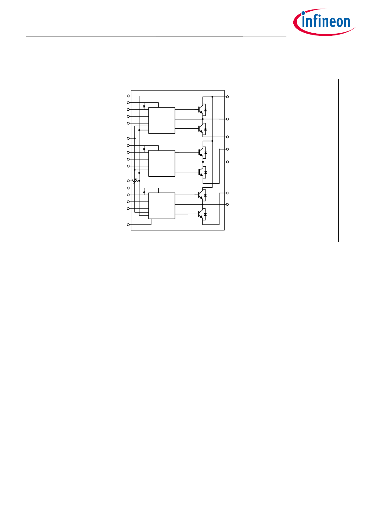
Internal Electrical Schematic
1 Internal Electrical Schematic
Figure 1 Internal electrical schematic.
Half-Bridge
HVIC
Half-Bridge
HVIC
Half-Bridge
HVIC
1 COM
2 V
B1
3 V
CC1
4 HIN1
5 LIN1
6 RFE
7 V
B2
8 V
CC2
9 HIN2
10 LIN2
11 VTH
12 V
B3
13 V
CC3
14 HIN3
15 LIN3
16 ITRIP
17 V+
18 U/V
S1
19 V
R1
20 V
R2
21 V/V
S2
22 V
R3
23 W/V
S3
Page 4
Final Datasheet 4 Revision 2.1
2019-07-15
CIPOS™ Micro
IM231-L6S1B / IM231-L6T2B
Pin Configuration
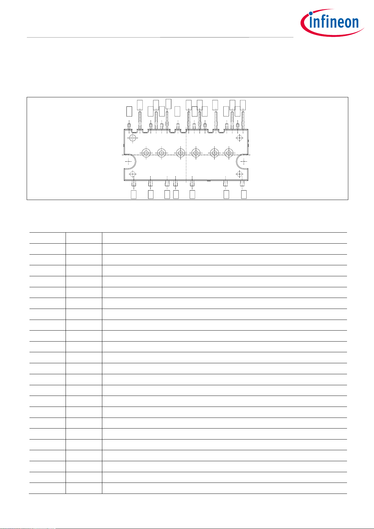
2 Pin Configuration
2.1 Pin Assignment
e
1
2
3
4
5
7
8
9
10
12
13
14
15
16
23
22
21
20
19
18
17
11
6
Figure 2 Module pinout
Table 2 Pin Assignment
Pin
Name
Description
1
COM
Logic ground
2
VB1
High side floating supply voltage 1
3
V
DD1
Low side control supply 1
4
HIN1
Logic Input for high side gate driver - Phase 1
5
LIN1
Logic Input for low side gate driver - Phase 1
6
RFE
RCIN / Fault / Enable
7
VB2
High side floating supply voltage 2
8
V
DD2
Low side control supply 2
9
HIN2
Logic input for high side gate driver - Phase 2
10
LIN2
Logic input for low side gate driver - Phase 2
11
VTH
Thermistor output
12
VB3
High side floating supply voltage 3
13
V
DD3
Low side control supply 3
14
HIN3
Logic Input for high side gate driver - Phase 3
15
LIN3
Logic Input for low side gate driver - Phase 3
16
ITRIP
Current protection pin
17
V+
Dc bus voltage positive
18
U/VS1
Output - phase 1, high side floating supply offset 1
19
VR1
Phase 1 low side emitter
20
VR2
Phase 2 low side emitter
21
V/VS2
Output - phase 2, high side floating supply offset 2
22
VR3
Phase 3 low side emitter
23
W/VS3
Output – phase 3, high side floating suppyl offset 3
Page 5
Final Datasheet 5 Revision 2.1
2019-07-15
CIPOS™ Micro
IM231-L6S1B / IM231-L6T2B
Pin Configuration
2.2 Pin Descriptions
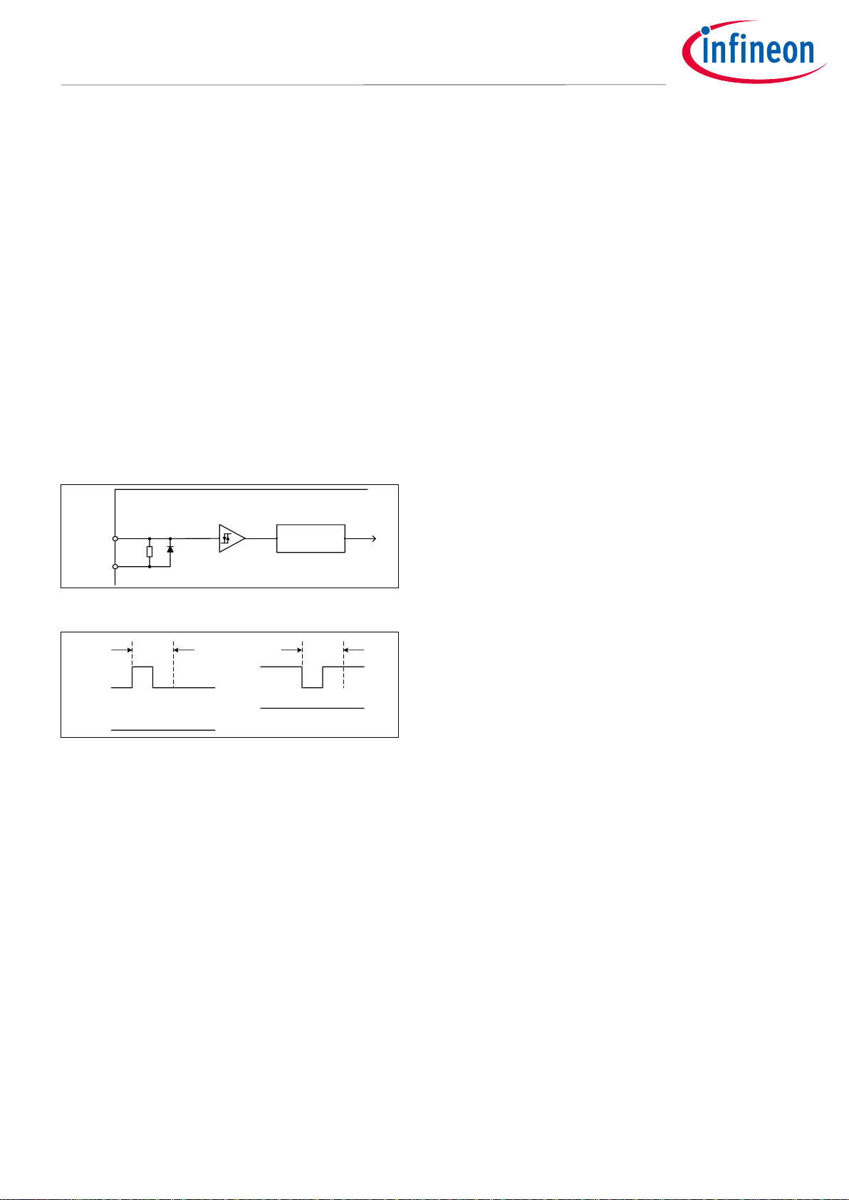
HIN(1,2,3) and LIN(1,2,3) (Low side and high side
control pins)
These pins are positive logic and they are
responsible for the control of the integrated IGBT.
The Schmitt-trigger input thresholds of them are
such to guarantee LSTTL and CMOS compatibility
down to 3.3V controller outputs. Pull-down resistor
of about 800k is internally provided to pre-bias
inputs during supply start-up and an ESD diode is
provided for pin protection purposes. Input
Schmitt-trigger and noise filter provide beneficial
noise rejection to short input pulses.
The noise filter suppresses control pulses which are
below the filter time T
FILIN
. The filter acts according
to Figure 4.
CIPOS
TM
INPUT NOISE
FILTER
M8.0
Schmitt-Trigger
SWITCH LEVEL
V
IH
; V
IL
COM
HINx
LINx
Figure 3 Input pin structure
HIN
LIN
HO
LO
low
high
t
FILIN
t
FILIN
a) b)
HIN
LIN
HO
LO
Figure 4 Input filter timing diagram
The integrated gate drive provides additionally a
shoot through prevention capability which avoids
the simultaneous on-state of the high-side and lowside switch of the same inverter phase. A minimum
deadtime insertion of typically 300ns is also
provided by driver IC, in order to reduce crossconduction of the external power switches.
VDD, COM (Low side control supply and reference)
VDD is the control supply and it provides power both
to input logic and to the output power stage. Input
logic is referenced to COM ground.
The under-voltage circuit enables the device to
operate at power on when a supply voltage of at
least a typical voltage of V
DDUV+
= 11.1V is present.
The IC shuts down all the gate drivers power
outputs, when the VDD supply voltage is below V
DDUV-
= 10.9V. This prevents the external power switches
from critically low gate voltage levels during onstate and therefore from excessive power
dissipation.
V
B(1,2,3)
and V
S(1,2,3)
(High side supplies)
VB to VS is the high side supply voltage. The high side
circuit can float with respect to COM following the
external high side power device emitter voltage.
Due to the low power consumption, the floating
driver stage is supplied by integrated bootstrap
circuit.
The under-voltage detection operates with a rising
supply threshold of typical V
BSUV+
= 11.1V and a falling
threshold of V
BSUV-
= 10.9V.
V
S(1,2,3)
provide a high robustness against negative
voltage in respect of COM. This ensures very stable
designs even under rough conditions.
V
R(1,2,3)
(Low side emitters)
The low side emitters are available for current
measurements of each phase leg. It is
recommended to keep the connection to pin COM as
short as possible in order to avoid unnecessary
inductive voltage drops.
VTH (Thermistor output)
A UL certified NTC resistor is integrated in the
module with one terminal of the chip connected to
COM and the other to VTH. When pulled up to a rail
voltage such as VDD or 3.3V by a resistor, the VTH pin
provides an analog voltage signal corresponding to
the temperature of the thermistor.
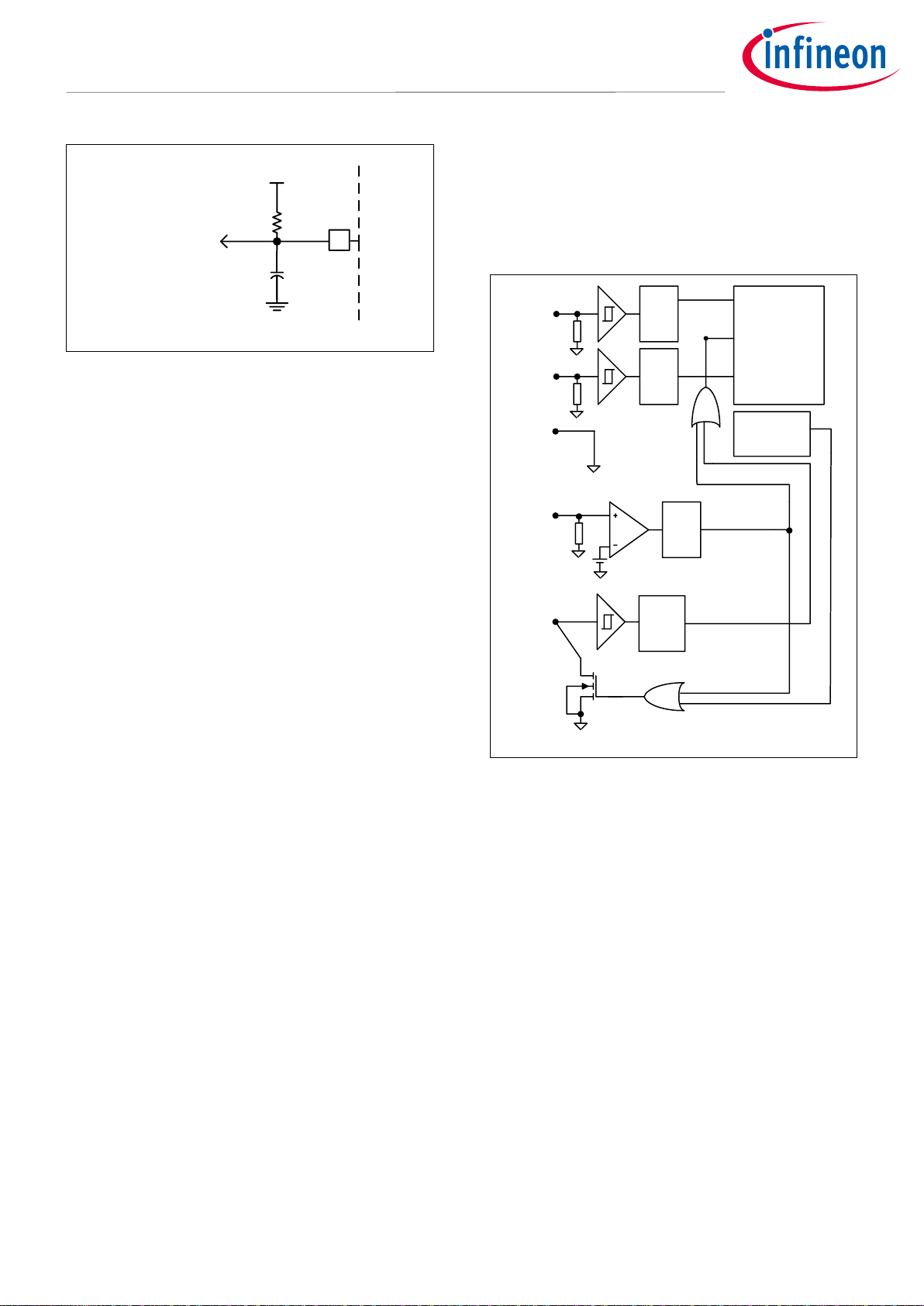
RFE (RCIN / Fault / Enable)
The RFE pin combines 3 functions in one pin: RCIN or
RC-network based programmable fault clear timer,
fault output and enable input.
The RFE pin is normally connected to an RC network
on the PCB per the schematic in Figure 5. Under
normal operating conditions, R
RCIN
pulls the RFE pin
to 3.3V, thus enabling all the functions in the IPM.
The microcontroller can pull this pin low to disable
the IPM functionality. This is is the Enable function.
Page 6
Final Datasheet 6 Revision 2.1
2019-07-15
CIPOS™ Micro
IM231-L6S1B / IM231-L6T2B
Pin Configuration
Figure 5 Typical PCB circuit connected to
the RFE pin
The Fault function allows the IPM to report a Fault
condition to the microncontroller by pulling the RFE
pin low in one of two situations. The first is an undervoltage condition on VDD and the second is when the
ITRIP pin sees a voltage rising above V
IT,TH+
.
The programmable fault clear timer function
provides a means of automatically re-enabling the
module operation a preset amount of time (T
FLT-CLR
)
after the fault condition has disappeared. Figure 6
shows the RFE-related circuit block diagram inside
the IPM.
The length of TFLT-CLR can be determined by using
the formula below.
V
RFE
(t) = 3.3V * (1 – e
-t/RC
)
T
FLT-CLR
= -R
RCIN
* C
RCIN
* ln(1-V
IN,TH+
/3.3V)
For example, if R
RCIN
is 1.2MΩ and C
RCIN
is 1nF, the T
FLT-
CLR
is about 1.7ms with V
IN,TH+
of 2.5V. It is also
important to note that C
RCIN
needs to be minimized in
order to make sure it is fully discharged in case of
over current event.
Since the ITRIP pin has a 500ns input filter, it is
appropriate to ensure that C
RCIN
will be discharged
below V
IN,TH-
by the open-drain MOSFET, after 350ns.
Therefore, the max C
RCIN
can be calculated as:
V
RFE
(t) = 3.3V * e
-t/RC
< V
IN,TH-
C
RCIN
< 500ns / ( - ln (V
IN,TH-
/ 3.3V) * R
RFE_ON
)
Consider V
IN,TH-
of 0.8V and R
RFE_ON
of 50ohm, C
RCIN
should be less than 7nF. It is also suggested to use a
R
RCIN
of between 0.5MΩ and 2MΩ.
Figure 6 RFE internal circuit structure
U/VS1, V/VS2, W/V
S3
(High side emitter and low side
collector)
These pins are motor U, V, W input pins.
V+ (Positive bus input voltage, Pin 23)
The high side IGBTs are connected to the bus
voltage. It is noted that the bus voltage should not
exceed 450V.
Input
Noise
filter
Input
Noise
filter
Deadtime &
Shoot-Through
Prevention
ITRIP
Noise
filter
HIN
LIN
COM
ITRIP
RFE
Noise
filter
VDD
Undervoltage
detection
+3.3V
R
RCIN
C
RCIN
6 RFE
IM231-L6
To Microcontroller
Page 7
Final Datasheet 7 Revision 2.1
2019-07-15
CIPOS™ Micro
IM231-L6S1B / IM231-L6T2B
Absolute Maximum Rating
3 Absolute Maximum Rating
3.1 Module
Table 3
Parameter
Symbol
Condition
Units
Storage temperature
T
STG
-40 ~ 150
°C
Operating case temperature
TC
-40 ~ 125
°C
Operating junction temperature
TJ
-40 ~ 150
°C
Isolation test voltage
V
ISO
1min, RMS, f = 60Hz
2000
V
3.2 Inverter
Table 4
Parameter
Symbol
Condition
Units
Max. blocking voltage
V
CES/VRRM
600
V
Output current
I
O
TC = 25°C 6 A
Peak output current
IOP
TC = 25°C, tp < 1ms
9
A
Peak power dissipation per IGBT
P
tot
TC = 25°C
10.5
W
Short circuit withstand time
T
SC
VDC = 360V, TJ = 150°C, VDD = 15V
Allowed number of short
circuits: <1000, time between
short circuits: >1s
3
μs
3.3 Control
Table 5
Parameter
Symbol
Condition
Units
Low side control supply voltage
V
DD
-0.3 ~ 20
V
Input voltage
V
IN
LIN, HIN,ITRIP,RFE
-0.3 ~ V
DD
V
High side floating supply voltage
(VB reference to VS)
V
BS
-0.3 ~ 20
V
Page 8

Final Datasheet 8 Revision 2.1
2019-07-15
CIPOS™ Micro
IM231-L6S1B / IM231-L6T2B
Thermal Characteristics
4 Thermal Characteristics
Table 6
Parameter
Symbol
Conditions
Min.
Typ.
Max.
Units
Junction-case thermal
resistance, all IGBTs
operating (per module)
R
TH(J-C)_M
-
2.4
2.8
°C/W
Junction-case thermal
resistance, all diodes
operating (per module)
R
TH(J-C)D_M
-
2.5
2.9
°C/W
Single IGBT thermal
resistance, junction-case
R
TH(J-C)
High side V-phase
IGBT
-
8.4
9.6
°C/W
Single diode thermal
resistance, junction-case
R
TH(J-C)D
High side V-phase
diode
-
9.3
10.8
°C/W
Page 9

Final Datasheet 9 Revision 2.1
2019-07-15
CIPOS™ Micro
IM231-L6S1B / IM231-L6T2B
Recommended Operating Conditions
5 Recommended Operating Conditions
Table 7
Parameter
Symbol
Min.
Typ.
Max.
Units
Positive DC bus input voltage
V+ - - 450
V
Low side control supply voltage
VDD
13.5
-
16.5
V
High side floating supply voltage
V
BS
12.5
-
17.5
V
Input voltage (LIN,HIN,ITRIP,RFE)
V
IN
0 - 5
V
PWM carrier frequency
F
PWM -
20 - kHz
External dead time between HIN & LIN
DT 1 - - µs
Voltage between COM and V
R(1,2,3)
V
COMR
-5 - 5
V
Minimum input pulse width
PW
IN(ON)
,
PW
IN(OFF)
1 - -
µs
Page 10

Final Datasheet 10 Revision 2.1
2019-07-15
CIPOS™ Micro
IM231-L6S1B / IM231-L6T2B
Static Parameters
6 Static Parameters
6.1 Inverter
(VDD-COM) = (VB - VS) = 15 V. TC = 25°C unless otherwise specified.
Table 8
Parameter
Symbol
Conditions
Min.
Typ.
Max.
Units
Collector-to-emitter
saturation voltage
V
CE(sat)
IC = 1A - 1.2 - V
IC = 3A
-
1.65
2.0
V
IC = 3A, TJ = 150℃
-
1.8 - V
Collector emitter leakage
current
I
CES
VIN = 0V, V+ = 600V
- - 80
µA
VIN = 0V, V+ = 600V, TJ
= 150°C
-
24 - µA
Diode forward voltage
V
F
IC = 1A - 1.2 - V
IC = 3A - 1.6
2.0
V
IC = 3A, TJ = 150℃
-
1.5 - V
6.2 Control
(VDD-COM) = (VB - VS) = 15 V. TC = 25°C unless otherwise specified. The VIN and IIN parameters are referenced to COM
and are applicable to all six channels. The V
DDUV
parameters are referenced to COM. The V
BSUV
parameters are
referenced to VS.
Table 9
Parameter
Symbol
Min.
Typ.
Max.
Units
Logic “1” input voltage (LIN, HIN)
V
IN,TH+
2.2 - -
V
Logic “0” input voltage (LIN, HIN)
V
IN,TH-
- - 0.8
V
VDD/V
BS
supply undervoltage, positive going
threshold
V
DD,UV+
,
V
BS,UV+
9.6
10.4
11.2
V
VDD/VBS supply undervoltage, negative going
threshold
V
DD,UV-
,
V
BS,UV-
8.6
9.4
10.2
V
VDD/VBS supply undervoltage lock-out
hysteresis
V
DDUVH
,
V
BSUVH
-
1.0 - V
RFE positive going threshold
V
RFE+
-
1.9
2.2
V
RFE negative going threshold
V
RFE-
0.8
1.1 - V
ITRIP positive going threshold
V
IT,TH+
0.475
0.500
0.525
V
ITRIP negative going threshold
V
IT,TH-
-
0.430 - V
ITRIP input hysteresis
V
IT,HYS
-
0.07 - V
Quiescent VBS supply current
I
QBS
- - 70
µA
Quiescent VDD supply current per channel
I
QDD
- - 2.6
mA
Input bias current VIN=5V for LIN, HIN
I
IN+
-
6.25
12.5
µA
Input bias current VIN=5V for RFE
I
IN,RFE+
- - 1
µA
Page 11

Final Datasheet 11 Revision 2.1
2019-07-15
CIPOS™ Micro
IM231-L6S1B / IM231-L6T2B
Static Parameters
Parameter
Symbol
Min.
Typ.
Max.
Units
Input bias current VIN=5V for ITRIP
I
ITRIP+
- 5 20
µA
Bootstrap resistance
R
BS
-
200
-
Ω
RFE low on resistance
R
RFE
-
34
60
Ω
Page 12

Final Datasheet 12 Revision 2.1
2019-07-15
CIPOS™ Micro
IM231-L6S1B / IM231-L6T2B
Dynamic Parameters
7 Dynamic Parameters
7.1 Inverter
(VDD-COM) = (VB - VS) = 15 V. TC = 25°C unless otherwise specified.
Table 10
Parameter
Symbol
Conditions
Min.
Typ.
Max.
Units
Input to output turn-on
propagation delay
T
ON
IC = 3A, V+ = 300V
-
641 - ns
Turn-on rise time
T
R
-
37 - ns
Turn-on switching time
T
C(on)
-
135 - ns
Input to output turn-off
propagation delay
T
OFF
IC = 3A, V+ = 300V
-
895 - ns
Turn-off fall time
T
F
-
80 - ns
Turn-off switching time
T
C(off)
-
82 - ns
RFE low to six switch turn-off
propagation delay
T
EN
VIN=0 or VIN=5V,
V
RFE
=5V
-
520 - ns
ITRIP to six switch turn-off
propagation delay
T
ITRIP
V+ = 300V,no cap
on RFE
-
1.3 - µs
Turn-on switching energy
E
ON
IC = 3A, V+ = 300V,
VDD = 15V, L = 5mH
-
86
-
µJ
Turn-off switching energy
E
OFF
-
31
-
Diode reverse recovery energy
E
REC
-
20
-
Diode reverse recovery time
T
RR
-
153 - ns
Turn-on switching energy
E
ON
IC = 3A, V+ = 300V,
VDD = 15V, L = 5mH
TJ = 150°C
-
129
-
µJ
Turn-off switching energy
E
OFF
-
50
-
Diode reverse recovery energy
E
REC
-
51
-
Diode reverse recovery time
T
RR
-
211 - ns
7.2 Control
(VDD-COM) = (VB - VS) = 15V. TC = 25°C unless otherwise specified.
Table 11
Parameter
Symbol
Conditions
Min.
Typ.
Max.
Units
Input filter time (HIN, LIN)
T
FIL,IN
V
IN
= 0 or VIN = 5V
-
300 - ns
Input filter time (ITRIP)
T
FIL,ITRIP
VIN=0 or VIN=5V
-
500 - ns
Internal dead time
DT
IC
V
IN
= 0 or VIN = 5V
-
300 - ns
Matching propagation delay
time (on and off) for same
phase high-side and low-side
M
T
External dead time
> 500ns
- - 50
ns
Page 13

Final Datasheet 13 Revision 2.1
2019-07-15
CIPOS™ Micro
IM231-L6S1B / IM231-L6T2B
Thermistor Characteristics
8 Thermistor Characteristics
Table 12
Parameter
Symbol
Conditions
Min.
Typ.
Max.
Units
Resistance
R
25
TC = 25°C, ±5% tolerance
44.65
47
49.35
kΩ
Resistance
R
125
TC = 125°C
1.27
1.39
1.51
kΩ
B-constant
(25/100)
B
±1% tolerance
-
4006 - K
Temperature
Range
-20 - 150
°C
Figure 7 Thermistor resistance – temperature curve, for R
EXT
=9.76kΩ, and thermistor resistance
variation with temperature.
+3.3V
R
EXT
R
V
TH
0.0
0.5
1.0
1.5
2.0
2.5
3.0
3.5
4.0
0 10 20 30 40 50 60 70 80 90 100 110 120 130 140 150
Thermistor Pin Readout Voltage VTH (V)
Thermistor Temperature TTH (°C)
max
typ
min
T
TH
[℃]
Rmin
[kΩ]
Rtyp
[kΩ]
Rmax
[kΩ]
50
15.448
16.432
17.436
60
10.483
11.194
11.924
70
7.245
7.765
8.302
80
5.092
5.477
5.876
90
3.648
3.937
4.237
100
2.653
2.872
3.101
110
1.957
2.125
2.301
120
1.462
1.592
1.729
125
1.269
1.384
1.505
Page 14

Final Datasheet 14 Revision 2.1
2019-07-15
CIPOS™ Micro
IM231-L6S1B / IM231-L6T2B
Mechanical Characteristics and Ratings
9 Mechanical Characteristics and Ratings
Table 13
Parameter
Symbol
Conditions
Min.
Typ.
Max.
Units
Comparative Tracking
Index
CTI
550 - -
V
Curvature of module
backside
BC
See Figure 9
-50 - 50
µm
Mounting Torque
τ
M3 screw & washer,
thermal grease
0.4
0.8
1.2
Nm
M3 screw & washer,
SIL-PAD 1500ST
-
0.6
1.0
Nm
Weight
W
-
3.0 - g
Page 15

Final Datasheet 15 Revision 2.1
2019-07-15
CIPOS™ Micro
IM231-L6S1B / IM231-L6T2B
Qualification Information
10 Qualification Information
Table 14
UL Certification
File number E252584
Moisture sensitivity level
(SOP 29 x 12 only)
MSL3
RoHS Compliant
Yes
Page 16

Final Datasheet 16 Revision 2.1
2019-07-15
CIPOS™ Micro
IM231-L6S1B / IM231-L6T2B
Diagrams & Tables
11 Diagrams & Tables
11.1 T
C
Measurement Point
Figure 8 T
C
measurement point
11.2 Backside Curvature Measurement Points
Figure 9 Curvature measurement points
12.20 mm
4.5 mm
0.50
0.50
0.50
+-
+
-
0.50
0.50
0.50
0.50
Page 17

Final Datasheet 17 Revision 2.1
2019-07-15
CIPOS™ Micro
IM231-L6S1B / IM231-L6T2B
Diagrams & Tables
11.3 Input-Output Logic Table
Figure 10 Module block diagram
Table 15
RFE
ITRIP
HIN1,2,3
LIN1,2,3
U,V,W
1 0 1 0 V+
1 0 0 1 0 1 0 0 0 ‡ 1 0 1 1 ‡ 1 1 x x
‡
0 x x x ‡
‡ Voltage depends on direction of phase current
Page 18

Final Datasheet 18 Revision 2.1
2019-07-15
CIPOS™ Micro
IM231-L6S1B / IM231-L6T2B
Diagrams & Tables
11.4 Switching Time Definitions
HINx
LINx
i
Cx
v
CEx
0.9V
2.1V
90%
10%
10%
10%
90%
t
off
t
f
t
on
t
r
t
c(off)
t
c(on)
10%
t
rr
10%
Figure 11 Switching times definition
Figure 12 ITRIP time waveform
Figure 13 Output disable timing diagram
RFE
50%
50%
U, V, W
T
EN
I
TRIP
LIN(U, V, W)
HIN(U, V, W)
T
FLT-CLR
50%
50%
U, V, W
50%
T
ITRIP
50%
RFE
50%
T
FLT
Page 19

Final Datasheet 19 Revision 2.1
2019-07-15
CIPOS™ Micro
IM231-L6S1B / IM231-L6T2B
Application Guide
12 Application Guide
12.1 Typical Application Schematic
HVICs
VCC
HIN1
HIN2
HIN3
LIN1
LIN2
LIN3
VTH
VB1
VB2 VB3
U/ VS1
V/ VS2
W/ VS3
Power
Supply
PWMWH
PWMVH
PWMUH
PWMVL
PWMWL
GK
VDC
IU/ISS
VSS
VDD
VSP
SPEED
COMMAND
COM
V+
iMotion™
IMC101T
PWMUL
0.25
CIPOS™ Micro
IM231-x6 Series
VDD
ITRIP
NTC
RFE
VR1
VR2
VR3
MOTOR
Figure 14 Application schematic
12.2 T
J
vs TTH
Figure 15 Typical T
J
vs TTH correlation
90
100
110
120
130
140
150
160
65 70 75 80 85 90 95 100 105 110 115
IGBT Junction Temperature
- °C
Internal Thermistor Temperature Equivalent Read Out - °C
T
J avg
= 1.06 x T
Therm
+ 26.48
Page 20

Final Datasheet 20 Revision 2.1
2019-07-15
CIPOS™ Micro
IM231-L6S1B / IM231-L6T2B
Application Guide
12.3 –V
S
Immunity
Figure 16 Negative transient V
s
SOA for integrated gate driver
-60
-50
-40
-30
-20
-10
0
0 100 200 300 400 500
Time (ns)
V
S
(V)
Page 21

Final Datasheet 21 Revision 2.1
2019-07-15
CIPOS™ Micro
IM231-L6S1B / IM231-L6T2B
Package Outline
13 Package Outline
13.1 DIP 29x12
Dimensions in mm
29.00±0.20
12.00±0.20
(2.275)
(1.165)
#17
#1
#23
#23
#17
(1.165)
1.27x21=26.67±0.30
27.60±0.15
1.95x13=25.35±0.30
2-R1.60
Detail "A"
ECN #
REV. DATE
DESCRIPTION CheckDRG.
SIGNATURE
SIGNATURE
SIGNATURE
SIGNATURE
APPROVED BY
UNIT
DRAWN BY
CHECKED BY
APPROVED BY
TITLE
DATE
A
B
C
D
8 7 6 5 4 3 2 1
ZONE
gEM Electronics Co.,Ltd.
The information contained herein is the exclusive property of GEM and shall not be
distributed, reproduced, or disclosed without prior written permission of GEM.
Polaris Li
A
NEW ISSUE
g
Ivan Yang
Ming Zhou
Polaris.Li HB Yang
G-70218
05/25/2017
B
Remove mark area. Change title. Add note 2 & 3.
DIP23P Case Outline
Detail "A"
6X Retractable Pin
5°
6°
5°
6°
R0.10 (ALL)
16-Max 0.70
16-0.50±0.10
#1
7-Max 0.80
7-0.60±0.10
(0.10)
(14.00)
14.00±0.30
(1.85)
(R0.40)
3.15±0.20
(R0.40)
0.50
+0.10
-0.05
3.00±0.30
LEAD ANGLE
0°~3°
6X Retractable Pin
(0.47)
(0.70)
(0.47)
(1.10)
2.90
+0.55
-0.45
5°
5°
6°
#16
4.50±0.15
6°
R0.10 (ALL)
R0.10 (ALL)
R0.10 (ALL)
R0.10 (ALL) R0.20 (ALL)
Note:
1. All Dimension Are In mm.
2. Dimensions are exclusive of burrs, mold flash,
and tie bar extrusions.
3. is Exposed Cu.
Exposed Cu
#16
6.05±0.20
Page 22

Final Datasheet 22 Revision 2.1
2019-07-15
CIPOS™ Micro
IM231-L6S1B / IM231-L6T2B
Package Outline
13.2 SOP 29x12
Dimensions in mm
29.00±0.20
12.00±0.20
(2.275)
(1.165)
7-Max 0.80
7-0.60±0.10
#23
#17
(1.165)
1.27x21=26.67±0.30
1.95x13=25.35±0.30
16-Max 0.70
16-0.50±0.10
#1 #16
17.00±0.20
(1.85)
3.15±0.20
0.15±0.10
0.50
+0.10
-0.05
5°±3°
(2.50)
1.50±0.20
(1.30)
(1.85)
Max 3.50
ECN #
REV. DATE
DESCRIPTION CheckDRG.
SIGNATURE
SIGNATURE
SIGNATURE
DRAWN BY
CHECKED BY
APPROVED BY
TITLE
A
B
C
D
8 7 6 5 4 3 2 1
ZONE
gEM Electronics Co.,Ltd.
The information contained herein is the exclusive property of GEM and shall not be
distributed, reproduced, or disclosed without prior written permission of GEM.
Polaris Li
A
NEW ISSUE
g
Ivan Yang
Polaris.Li
HB Yang
G-70219
05/25/2017
B
Remove mark area. Change title. Add note 2 & 3.
SOP23P Case Outline
(0.47)
(0.70)
(0.47)
(1.10)
Detail "A"
Detail "A"
6X Retractable Pin
5°
6°
5°
6°
R0.10 (ALL)
6X Retractable Pin
7.55
7.55
1.95
1.27
0.64
2.80
1.20
2.80
0.90
1.64
0.75
#17
#1
#16
#23
2.48
Land Pattern
27.60±0.15
2-R1.60
4.50±0.15
5°
6°
5°
6°
#17
#1
#16
#23
#16
R0.10 (ALL)
R0.10 (ALL)
R0.10 (ALL)
R0.10 (ALL)
R0.20 (ALL)
Note:
1. All Dimension Are In mm.
2. Dimensions are exclusive of burrs, mold flash,
and tie bar extrusions.
3. is Exposed Cu.
Exposed Cu
(R0.40)
Page 23

Final Datasheet 23 Revision 2.1
2019-07-15
CIPOS™ Micro
IM231-L6S1B / IM231-L6T2B
Revision History
14 Revision History
Major changes since the last revision
Page or Reference
Description of change
Page 21 -22
Updated font size for Package Outline drawing
Page 24

Published by
Infineon Technologies AG
81726 München, Germany
© 2019 Infineon Technologies AG.
All Rights Reserved.
Do you have a question about this
document?
Email: erratum@infineon.com
Document reference
IMPORTANT NOTICE
The information given in this document shall in no
event be regarded as a guarantee of conditions or
characteristics (“Beschaffenheitsgarantie”) .
With respect to any examples, hints or any typical
values stated herein and/or any information
regarding the application of the product, Infineon
Technologies hereby disclaims any and all
warranties and liabilities of any kind, including
without limitation warranties of non-infringement of
intellectual property rights of any third party.
In addition, any information given in this document
is subject to customer’s compliance with its
obligations stated in this document and any
applicable legal requirements, norms and standards
concerning customer’s products and any use of the
product of Infineon Technologies in customer’s
applications.
The data contained in this document is exclusively
intended for technically trained staff. It is the
responsibility of customer’s technical departments
to evaluate the suitability of the product for the
intended application and the completeness of the
product information given in this document with
respect to such application.
For further information on the product, technology,
delivery terms and conditions and prices please
contact your nearest Infineon Technologies office
(www.infineon.com).
WARNINGS
Due to technical requirements products may contain
dangerous substances. For information on the types
in question please contact your nearest Infineon
Technologies office.
Except as otherwise explicitly approved by Infineon
Technologies in a written document signed by
authorized representatives of Infineon
Technologies, Infineon Technologies’ products may
not be used in any applications where a failure of the
product or any consequences of the use thereof can
reasonably be expected to result in personal injury.
Edition 2018-03-02
Trademarks
All referenced product or service names and trademarks are the property of their respective owners.
 Loading...