

Page 1
r
r
r
r
.
.
)
)
FEATURES
DUAL CHANNEL
QUAD CHANNEL
PHOTOTRANSISTOR OPTOCOUPLER
ILD615
ILQ615
• Identical Channel to Channel Footprint
• Current Transfer Ratio (CTR) Range at
I
=10 mA
F
ILD/Q615-1: 40 – 80% Min.
ILD/Q615-2: 63 – 125% Min.
ILD/Q615-3: 100 – 200% Min.
ILD/Q615-4: 160 – 320% Min.
• Guaranteed CTR at I
=1 mA
F
ILD/Q615-1: 13% Min.
ILD/Q615-2: 22% Min.
ILD/Q615-3: 34% Min.
ILD/Q615-4: 56% Min.
• High Collector-Emitter Voltage BV
CEO
• Dual and Quad Packages Feature:
- Reduced Board Space
- Lower Pin and Parts Count
- Better Channel to Channel CTR Match
- Improved Common Mode Rejection
=70 V
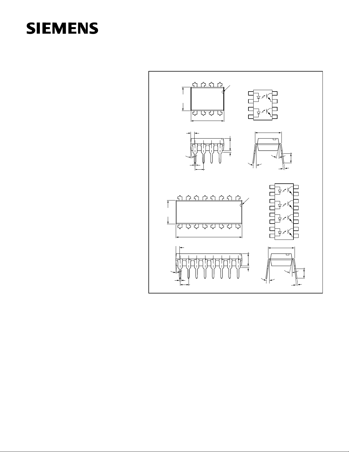
Dimensions in inches (mm)
.268 (6.81)
.255 (6.48)
.390 (9.91)
.379 (9.63)
.045 (1.14)
.030 (.76)
4°
Typ.
.022 (.56)
.018 (.46)
34
12
65
87
.100 (2.54) Typ.
Pin One I.D.
Anode
Cathode
Anode
Cathode
.150 (3.81)
.130 (3.30)
.040 (1.02)
.030 (.76 )
1
2
3
4
.305 Typ.
(7.75) Typ.
10° Typ.
3°–9°
.012 (.30)
.008 (.20)
8
7
6
5
Collector
Emitter
Collector
Emitter
.135 (3.43)
.115 (2.92)
• Field-Effect Stable by TRIOS (TR ansparent IO n
S hield )
• Isolation Test Voltage from Double Molded
Package, 5300 VAC
RMS
• UL Approval #E52744
• VDE #0884 Available with Option 1
Maximum Ratings (Each Channel)
Emitter
Reverse Voltage................................................ 6 V
Forward Current........................................... 60 mA
Surge Current .................................................1.5 A
Power Dissipation ......................................100 mW
Derate Linearly from 25 °
C ................... 1.33 mW/ ° C
Detector
Collector-Emitter Reverse Voltage .................. 70 V
Emitter-Collector Reverse Voltage .................... 7 V
Collector Current.......................................... 50 mA
268 (6.81)
255 (6.48)
4°
Typ.
.022 (.56)
.018 (.46)
.045 (1.14)
.030 (.76)
.100 (2.54) Typ.
.790 (20.07)
.779 (19.77 )
Pin
One
I.D.
.150 (3.81)
.130 (3.30)
.040 (1.02)
.030 (.76 )
Anode
Cathode
Anode
Cathode
Anode
Cathode
Anode
Cathode
1
2
3
4
5
6
7
8
.305 Typ.
(7.75) Typ.
10° Typ.
3°–9°
.012 (.30)
.008 (.20)
16
Collecto
15
Emitter
Collecto
14
Emitter
13
Collecto
12
Emitter
11
Collecto
10
Emitter
9
.135 (3.43
.115 (2.92
Collector Current (t <1 ms) .........................100 mA
Power Dissipation ......................................150 mW
Derate Linearly from 25 °
C........................ 2 mW/ ° C
Package
Storage Temperature................... –55 ° C to +150 ° C
Operating Temperature............... –55 °
C to +100 ° C
Junction Temperature....................................100 °
Soldering Temperature
(2 mm distance from case bottom)...........260 °
Package Power Dissipation, ILD615..........400 mW
Derate Linearly from 25 °
C..................5.33 mW/ ° C
Package Power Dissipation, ILQ615 .........500 mW
Derate Linearly from 25 °
Isolation Test V oltage (t=1 sec.)........5300 VAC
C................. 6.67 mW/ ° C
RMS
Creepage............................................... 7 mm min.
Clearance............................................... 7 mm min.
Isolation Resistance
V
=500 V, T
IO
V
=500 V, T
IO
=25 ° C............................... ≥ 10
A
=100 ° C............................. ≥ 10
A
12
11
DESCRIPTION
The ILD/Q615 are multi-channel phototransistor optocouplers that use GaAs
IRLED emitters and high gain NPN phototransistors. These devices are constructed using over/under leadframe optical coupling and double molded
insulation technology resulting a Withstand Test Voltage of 7500 VAC
C
and a Working Voltage of 1700 VAC
The binned min./max. and linear CTR characteristics combined with the
C
TRIOS (TRansparent IOn Shield) field-effect process make these devices
RMS
.
well suited for DC or AC voltage detection. Eliminating the phototransistor
base connection provides added electrical noise immunity from the transients found in many industrial control environments.
Because of guaranteed maximum non-saturated and saturated switching
characteristics, the ILD/Q615 can be used in medium speed data I/O and
control systems. The binned min./max. CTR specification allow easy worst
case interface calculations for both level detection and switching applica-
Ω
tions. Interfacing with a CMOS logic is enhanced by the guaranteed CTR at
Ω
an I
=1 mA.
F
PEAK
See Appnote 45, “How to Use Optocoupler Normalized Curves.”
5–1
Page 2
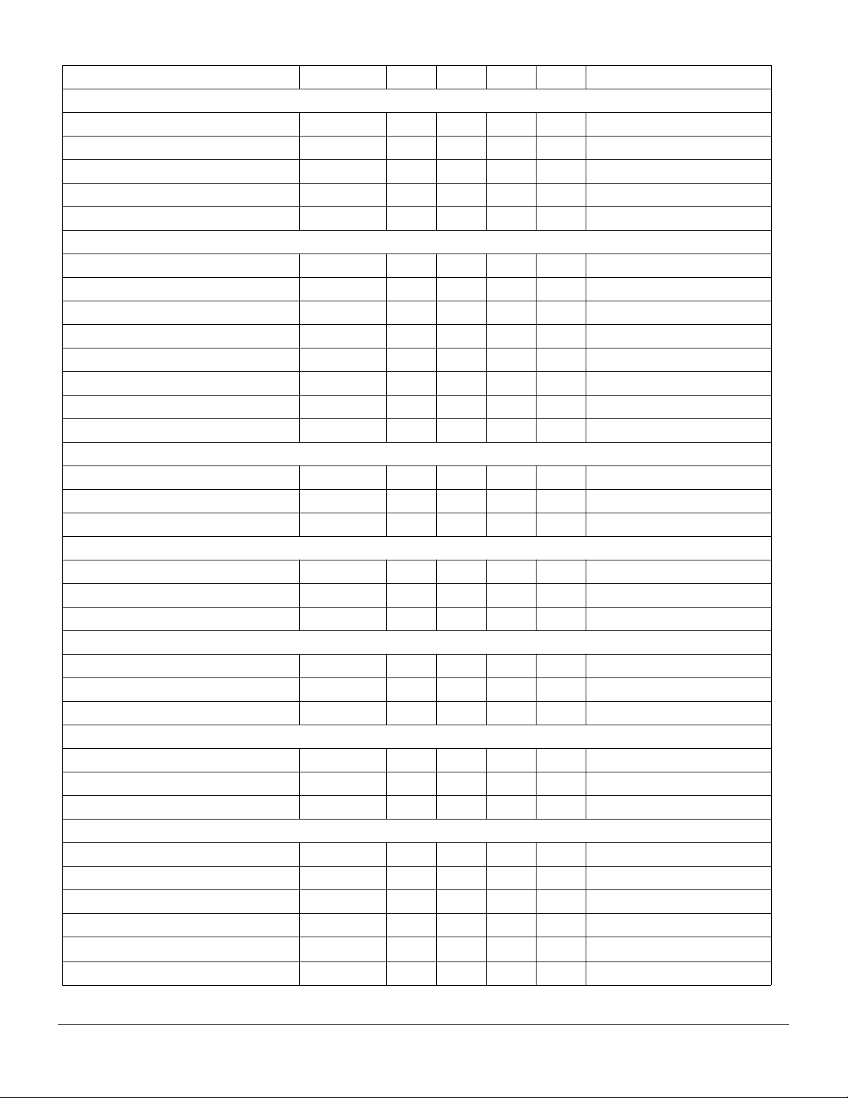
Characteristics, T
=25 ° C
A
Symbol Min. Typ. Max. Unit Condition
Emitter
Forward Voltage V
Breakdown Voltage V
Reverse Current I
Capacitance C
Thermal Resistance, Junction to Lead R
F
BR
F
O
THJL
1 1.15 1.3 V I
630 VI
0.01 10
µ AV
25 pF V
750
° C/W
F
R
R
R
Detector
Capacitance C
Collector-Emitter Leakage Current, -1, -2 I
Collector-Emitter Leakage Current, -3, -4 I
CEO
CEO
Collector-Emitter Breakdown Voltage BV
Emitter-Collector Breakdown Voltage BV
Thermal Resistance, Junction to Lead R
CE
CEO
ECO
THJL
70 V I
7VI
6.8 pF V
250nAV
5 100 nA V
500
° C/W
CE
CE
CE
CE
E
Package T ransfer Characteristics
Channel/Channel CTR Match CTRX/CTRY 1 to 1 2 to 1 I
F
ILD/Q615-1
Saturated Current Transfer Ratio CTR
Current Transfer Ratio CTR
Current Transfer Ratio CTR
CEsat
CE
CE
40 60 80 % I
13 30 % I
25 % I
F
F
F
ILD/Q615-2
Saturated Current Transfer Ratio CTR
Current Transfer Ratio CTR
Current Transfer Ratio CTR
CEsat
CE
CE
63 80 125 % I
22 45 % I
40 % I
F
F
F
ILD/Q615-3
Saturated Current Transfer Ratio CTR
Current Transfer Ratio CTR
Current Transfer Ratio CTR
CEsat
CE
CE
100 150 200 % I
34 70 % I
60 % I
F
F
F
ILD/Q615-4
Saturated Current Transfer Ratio CTR
Current Transfer Ratio CTR
Current Transfer Ratio CTR
CEsat
CE
CE
160 200 320 % I
56 90 % I
100 % I
F
F
F
Isolation and Insulation
Common Mode Rejection, Output High CMH 5000 V/ µ sV
Common Mode Rejection, Output Low CML 5000 V/ µ sV
Common Mode Coupling Capacitance C
CM
0.01 pF
Package Capacitance CI-O 0.8 pF V
Insulation Resistance R
S
10
14
Ω VIO=500 V, TA=25°C
CM
CM
IO
Channel to Channel Isolation 500 VAC
=10 mA
=10 µ A
=6 V
=0 V, f=1 MHz
=5 V, f=1 MHz
=10 V
=10 V
=0.5 mA
=0.1 mA
=10 mA, V
=10 mA, V
=10 mA, V
=1 mA, V
=10 mA, V
=10 mA, V
=1 mA, V
=10 mA, V
=10 mA, V
=1 mA, V
=10 mA, V
=10 mA, V
=1 mA, V
=50 V
=50 V
CE
CE
CE
CE
CE
CE
CE
CE
CE
CE
CE
CE
CE
P-P
P-P
=0 V, f=1 MHz
=5 V
=0.4 V
=5 V
=5 V
=0.4 V
=5 V
=5 V
=0.4 V
=5 V
=5 V
=0.4 V
=5 V
=5 V
, R
, R
=1 k Ω , I
L
=1 k Ω , I
L
=0 mA
F
=10 mA
F
5–2
ILD/Q615
Page 3
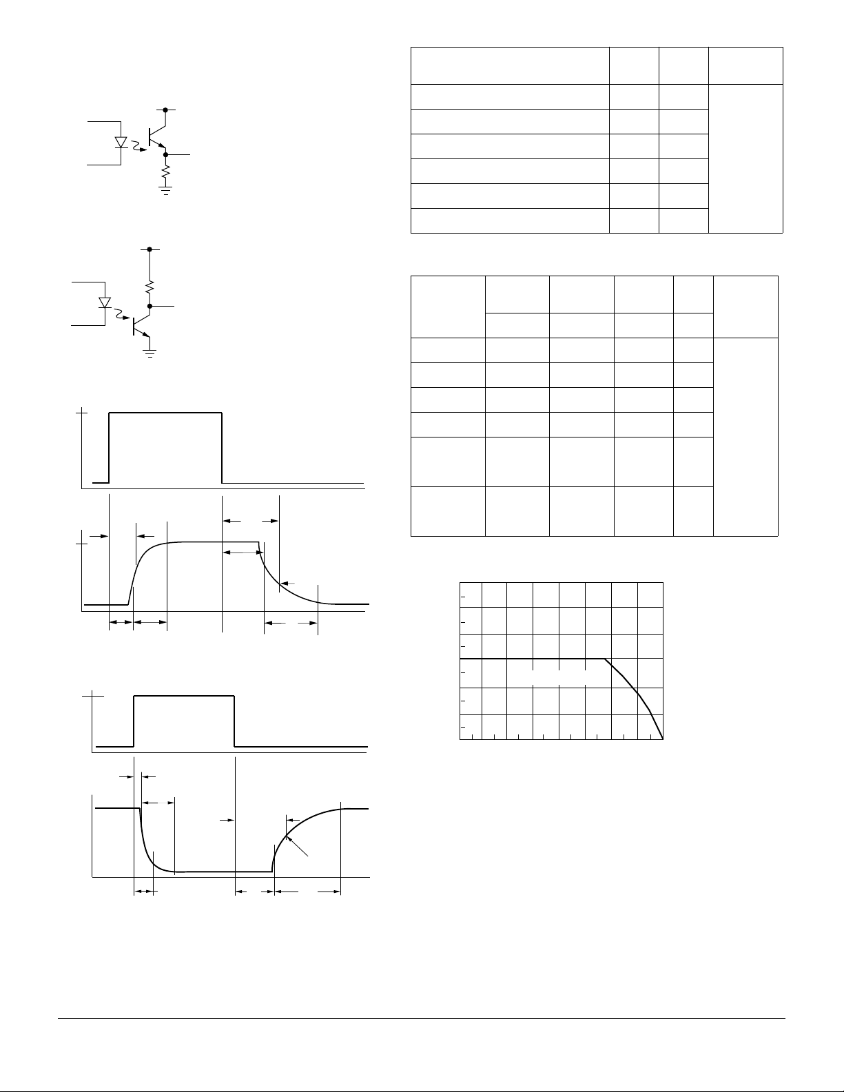
Switching Times
I
V
F
D
V
I
V
0
Figure 1. Non-saturated switching timing
VCC=5 V
=10 mA
F
F=10 KHz,
DF=50%
Figure 2. Saturated switching timing
=10 KHz,
F=50%
RL=75 Ω
VCC=5
R
L
V
V
O
O
Parameter Typ. Unit Test
t
ON
t
R
t
OFF
t
F
t
Propagation H-L (50% of VPP) 1.1 µs
PHL
t
Propagation L-H 2.5 µs
PHL
Parameter-1IF=20 mA
Typ. Typ. Typ. Unit
-1,-3
IF=10 mA-4IF=5mA Test
3.0 µs
2.0 µs
2.3 µs
2.0 µs
Condition
RL=75 Ω
IF=10 mA
VCC=5 V
Condition
Figure 3. Non-saturated switching timing
F
t
t
0
PLH
t
D
t
R
PHL
t
S
Figure 4. Saturated switching timing
I
F
t
D
t
O
R
t
PLH
t
F
50%
t
ON
t
R
t
OFF
t
F
t
PHL
Propagation
H-L
t
PLH
Propagation
L-H
3.0 4.3 6.0 µs
2.0 2.8 4.6 µs
RL=1 Ω
18 25 25 µs
VCC=5 V
11 14 15 µs
VTH=1.5 V
1.6 2.6 5.4 µs
8.6 7.2 7.4 µs
Figure 5. Maximum LED current versus ambient temperature
120
100
80
60
40
20
0
IF - Maximum LED Current - mA
--60 -40 -20 0 20 40 60 80 10
TJ (MAX)=100°C
Ta - Ambient Temperature - °C
t
PHL
t
S
VTH=1.5 V
t
F
5–3
ILD/Q615
Page 4
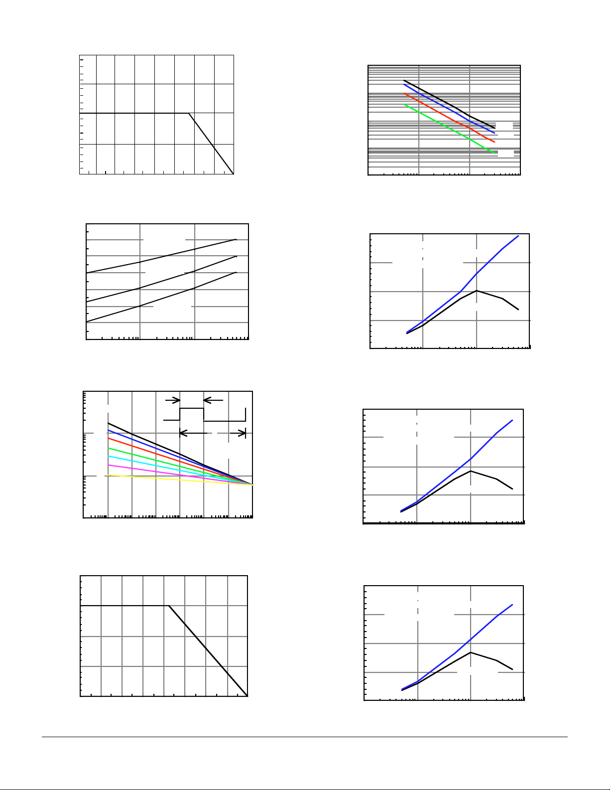
Figure 6. Maximum LED power dissipation
0
200
Figure 10. Maximum collector current ver sus collector
voltage
1000
150
100
- LED Power - mW
50
LED
P
0
--60 -40 -20 0 20 40 60 80 10
Ta - Ambient Temperature - °C
Figure 7. Forward voltage versus forward current
1.4
1.3
Ta = -55°C
1.2
1.1
Ta = 25°C
1.0
0.9
Ta = 85°C
0.8
VF - Forward Voltage - V
0.7
100101.1
IF - Forward Current - mA
100
10
1
Ice - Collector Current - mA
.1
.1 1 10 100
Vce - Collector-Emitter Voltage - V
Rth = 500°C/W
25°C
50°C
75°C
90°C
Figure 11. Normalization factor for non-saturated
and saturated CTR TA=25°C versus if
2.0
Normalized to:
Vce = 10V, IF = 5mA, Ta = 25°C
1.5
1.0
0.5
CTRNF - Normalized CTR Factor
0.0
CTRce(sat) Vce = 0.4V
NCTRce
NCTRce(sat)
Ta = 25°C
.1 1 10 100
IF - LED Current - mA
Figure 8. Peak LED current versus pulse detection, Tau
10000
Duty Factor
.005
1000
If(pk) - Peak LED Current - mA
.01
.02
.05
.1
.2
.5
100
10
10-610-510-410-310-210-110010
t - LED Pulse Duration - s
τ
t
τ
DF = /t
1
Figure 9. Maximum detector power dissipation
200
150
100
50
DET
P - Detector Power - mW
0
-60 -40 -20 0 20 40 60 80 100
Ta - Ambient Temperature - °C
Figure 12. Normalization factor for non-saturated
and saturated CTR T
2.0
Normalized to:
1.5
1.0
0.5
CTRNF - Normalized CTR Factor
0.0
Vce = 10V, IF = 5mA, Ta = 25°C
CTRce(sat) Vce = 0.4V
.1 1 10 100
=50°C versus if
A
NCTRce
NCTRce(sat)
IF - LED Current - mA
Ta = 50°C
Figure 13. Normalization factor for non-saturated
and saturated CTR T
2.0
Normalized to:
Vce = 10V, IF = 5mA, Ta = 25°C
1.5
1.0
0.5
CTRNF - Normalized CTR Factor
0.0
CTRce(sat) Vce = 0.4V
.1 1 10 100
=70°C versus if
A
NCTRce
NCTRce(sat)
IF - LED Current - mA
Ta = 70°C
5–4
ILD/Q615
Page 5
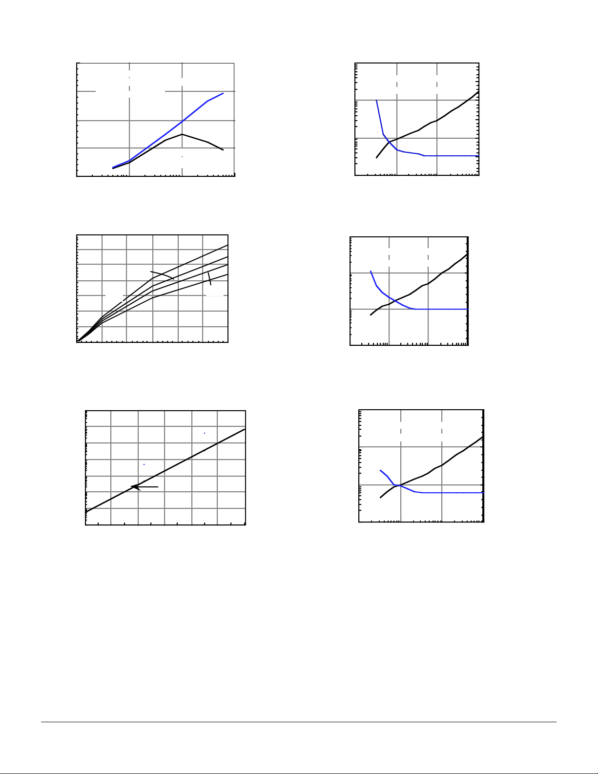
Figure 14. Normalization factor for non-saturated
and saturated CTR T
2.0
Normalized to:
Vce = 10V, IF = 5mA, Ta = 25°C
1.5
1.0
CTRce(sat) Vce = 0.4V
=85°C versus if
A
NCTRce
Figure 17. -1 Propagation delay versus collector load resistor
1000
Ta = 25°C, IF = 10mA
Vcc = 5V, Vth = 1.5V
100
tPLH
4.0
3.5
3.0
2.5
0.5
CTRNF - Normalized CTR Factor
0.0
.1 1 10 100
IF - LED Current - mA
NCTRce(sat)
Ta=100°C
Ta = 100°C
Figure 15. Collector-emitter current ver sus temperature
and LED current
35
30
25
50°C
20
15
10
25°C
85°C
70°C
5
0
Ice - Collector Current - mA
6050403020100
IF - LED Current - mA
Figure 16. Collector-emitter leakage versus
temperature
5
10
4
10
3
10
2
10
1
10
0
10
-1
10
Iceo - Collector-Emitter - nA
-2
10
Vce = 10V
TYPICAL
100806040200-20
Ta - Ambient Temperature - °C
10
tPLH - Propaga tion Low-High - µs
1
.1 1 10 100
RL - Load Resistor - KΩ
tP H L
2.0
1.5
1.0
tPHL - Propagation High-Low - µs
Figure 18. -2, -3 Propagation delay versus collector
load resistor
1000
Ta = 25°C, IF = 10mA
Vcc = 5V, Vth = 1.5V
100
tPLH
10
1
tPLH - Propagation Low-High - µs
.1 1 10 100
RL - Collector Load Resistor - KΩ
tPHL
2.5
2.0
1.5
1.0
tPHL - Propagation High-Low - µs
Figure 19. -4 Propagation delay versus collector
load resistor
1000
Ta = 25°C, IF = 10mA
Vcc = 5V, Vth = 1.5V
100
tPLH
10
1
tPLH - Propagation Low-High - µs
.1 1 10 100
RL - Collector Load Resistor - KΩ
tPHL
2.5
2.0
1.5
1.0
tPHL - Propagation High-Low - µs
5–5
ILD/Q615
 Loading...