

Page 1
3648 × 3pixel CCD Linear Sensor (Color)
For the availability of this product, please contact the sales office.
Description
The ILX516K is a reduction type CCD linear sensor
developed for color image scanner. This sensor
reads legal-size documents at a density of 400 DPI.
Features
• Number of effective pixels:
10944 pixels (3648 pixels × 3)
• Pixel size: 8µm × 8µm (8µm pitch)
• Distance between line: 64µm (8 Lines)
• Single-sided readout
• Ultra low lag / High sensitivity
• Single 12V power supply
• Input clock pulse: CMOS 5V drive
• Number of output 3 (R, G, B)
• Package: 22 pin cer-DIP (400 mil)
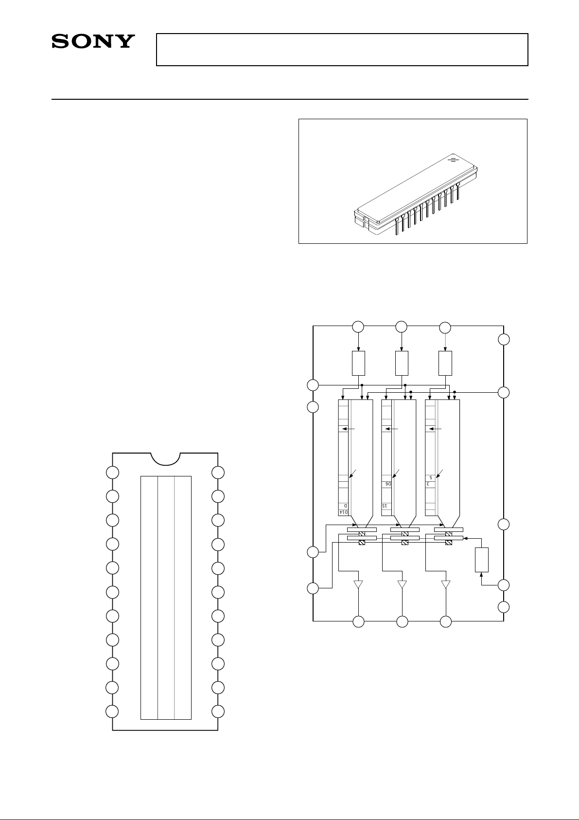
Block Diagram
ILX516K
22 pin DIP (Cer-DIP)
φROG-B
13
φROG-G
12
φROG-R
10
11
Absolute Maximum Ratings
• Supply voltage VDD 15 V
• Operating temperature –10 to +55 °C
• Storage temperature –30 to +80 °C
Pin Configuration (Top View)
VOUT-R
GND
φRS
φLH
GND
NC
NC
φ1
NC
1
2
3
4
5
6
7
8
9
22
21
20
19
18
17
16
15
14
VOUT-G
VOUT-B
VDD
NC
NC
NC
DD
V
φ2
NC
Driver
15
D75
16
4
20
VDD φLH VDD φ2
Blue
D64
S1
D63
D15
D14
S3648
Read Out Gate
CCD Register
21
VOUT-B
Green
D75
D64
S1
D63
D15
D14
Driver
S3648
Red
Read Out Gate
CCD Register
22
VOUT-G
D75
D64
S1
D63
D15
D14
Driver
S3648
Read Out Gate
CCD Register
1
VOUT-R
Driver
8
5
3
2
GND φRS GND φ1 GND
-R
φROG
GND
10
11
13
3648 R 1
3648 B 1
3648 G 1
12
φROG
φROG-G
-B
Sony reserves the right to change products and specifications without prior notice. This information does not convey any license by
any implication or otherwise under any patents or other right. Application circuits shown, if any, are typical examples illustrating the
operation of the devices. Sony cannot assume responsibility for any problems arising out of the use of these circuits.
– 1 –
E95813-PK
Page 2
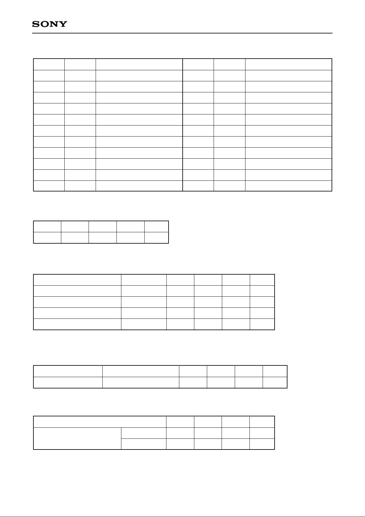
Pin Description
Pin No. Symbol Description Pin No. Symbol Description
ILX516K
1
2
3
4
5
6
7
8
9
10
11
VOUT-R
GND
φRS
φLH
GND
NC
NC
φ1
NC
φROG-R
GND
Signal out (red)
GND
Clock pulse input
Clock pulse input
GND
NC
NC
Clock pulse input
NC
Clock pulse input
GND
Recommended Supply Voltage
Item
VDD
Min.
11.4
Typ.
12.0
Max.
12.6
Unit
V
12
13
14
15
16
17
18
19
20
21
22
φROG-G
φROG-B
NC
φ2
VDD
NC
NC
NC
VDD
VOUT-B
VOUT-G
Clock pulse input
Clock pulse input
NC
Clock pulse input
12V power supply
NC
NC
NC
12V power supply
Signal out (blue)
Signal out (green)
Clock Characteristics
Item
Input capacity of φ1, φ2
Input capacity of φLH
Input capacity of φRS
Input capacity of φROG
∗
It indicates that φROG-R, φROG-G, φROG-B as φROG.
∗
Symbol
Cφ1, Cφ2
CφLH
CφRS
CφROG
Clock Frequency
Item Symbol
φ1, φ2, φLH, φRS fφ1, fφ2, fφLH, fφRS
Input Clock Pulse Voltage Condition
Item
φ1, φ2, φLH, φRS, φROG
pulse voltage
High level
Low level
Min.
—
—
—
—
Min.
4.75
—
Min.
—
Typ.
600
10
10
10
Typ.
5.0
0
Typ.
1
Max.
—
—
—
—
Max.
5.25
0.1
Max.
5
Unit
pF
pF
pF
pF
Unit
MHz
Unit
V
V
– 2 –
Page 3
ILX516K
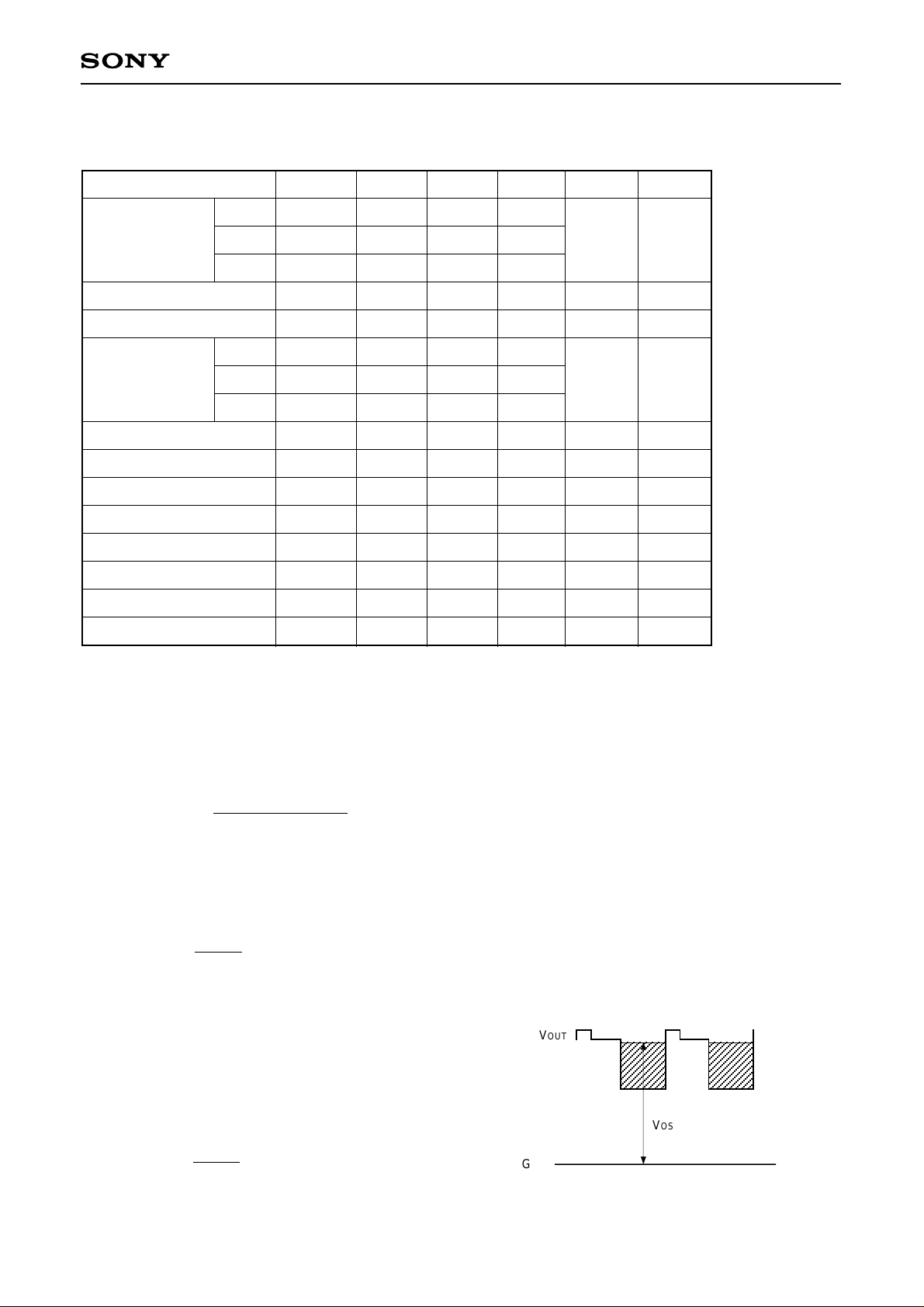
Electrooptical Characteristics (Note 1)
Ta = 25°C, VDD = 12V, fφRS = 1MHz, Input clock = 5Vp-p, Light source = 3200K, IR cut filter CM-500S (t = 1.0mm)
Item Symbol Min. Typ. Max. Unit Remarks
Red
Sensitivity
Green
Blue
Sensitivity nonuniformity
Saturation output voltage
Red
Saturation
exposure
Green
Blue
Dark voltage average
Dark signal nonuniformity
Image lag
Supply current
Total transfer efficiency
Output impedance
Offset level
Dynamic range
RR
RG
RB
PRNU
VSAT
SER
SEG
SEB
VDRK
DSNU
IL
IVDD
TTE
ZO
VOS
DR
1.3
2.1
1.6
—
2
0.74
0.46
0.58
—
—
—
—
92
—
—
1000
2.0
3.2
2.5
4
3.2
1.6
1
1.28
0.3
1.5
0.02
26
98
250
6.5
10670
2.7
4.3
3.4
20
—
—
—
—
2
5
—
50
—
—
—
—
V/(lx · s)
%
V
lx · s
mV
mV
%
mA
%
Ω
V
—
Note 2
Note 3
Note 4
Note 5
Note 6
Note 6
Note 7
—
—
—
Note 8
Note 9
Note
1) In accordance with the given electrooptical characteristics, the black level is defined as the average value
of D2, D3 to D12.
2) For the sensitivity test light is applied with a uniform intensity of illumination.
3) PRNU is defined as indicated below. Ray incidence conditions are the same as for Note 2.
VOUT-G = 500mV (Typ.)
PRNU = × 100 [%]
(VMAX – VMIN) /2
VAVE
Where the 3648 pixels are divided into blocks of 114. The maximum output of each block is set to VMAX,
the minimum output to VMIN and the average output to VAVE.
4) Use below the minimum value of the saturation output voltage.
5) Saturation exposure is defined as follows.
SE =
VSAT
R
Where R indicates RR, RG, RB, and SE indicates SER, SEG, SEB.
6) Optical signal accumulated time τint stands at 10ms.
7) VOUT-G = 500mV (Typ.)
VOUT
8) Vos is defined as indicated bellow.
VOUT indicates VOUT-R, VOUT-G, and VOUT-B.
9) Dynamic range is defined as follows.
DR =
VSAT
VDRK
GND
VOS
When the optical signal accumulated time is shorter, the dynamic range gets wider because the optical
signal accumulated time is in proportion to the dark voltage.
– 3 –
Page 4
ILX516K
3723
D75
D71
D70
D65
D64
S3648
S3647
S3646
S2
S1
D63
D62
D61
D15
D14
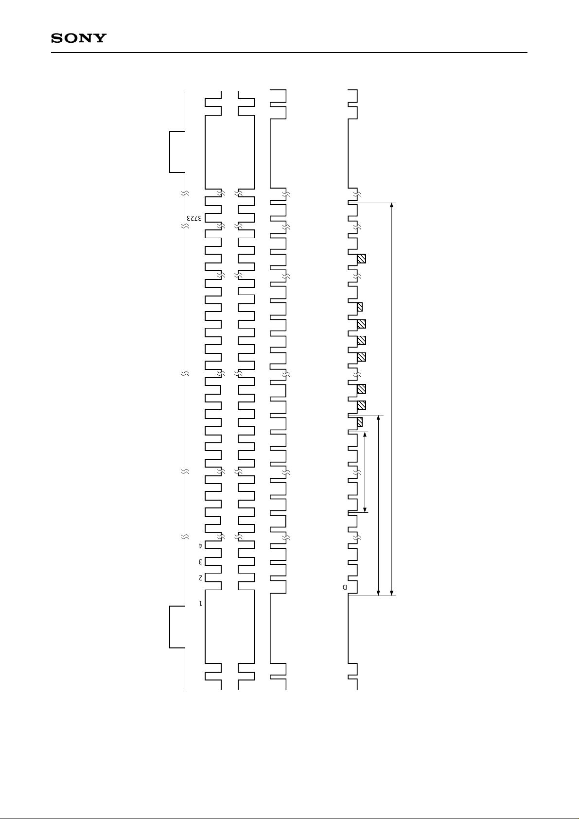
Optical black (49 pixels)
D13
1-line output period (3723 pixels)
Clock Timing Chart 1
5
0
φROG
4
3
2
1
5
0
5
0
5
0
D3
D2
D1
Dummy signal (63 pixels)
OUT indicates VOUT-R, VOUT-G, VOUT-B.
V
Note) The transfer pulses (φ1, φ2, φLH) must have more than 3723 cycles.
φ1
φLH
φ2
φRS
OUT
V
– 4 –
Page 5
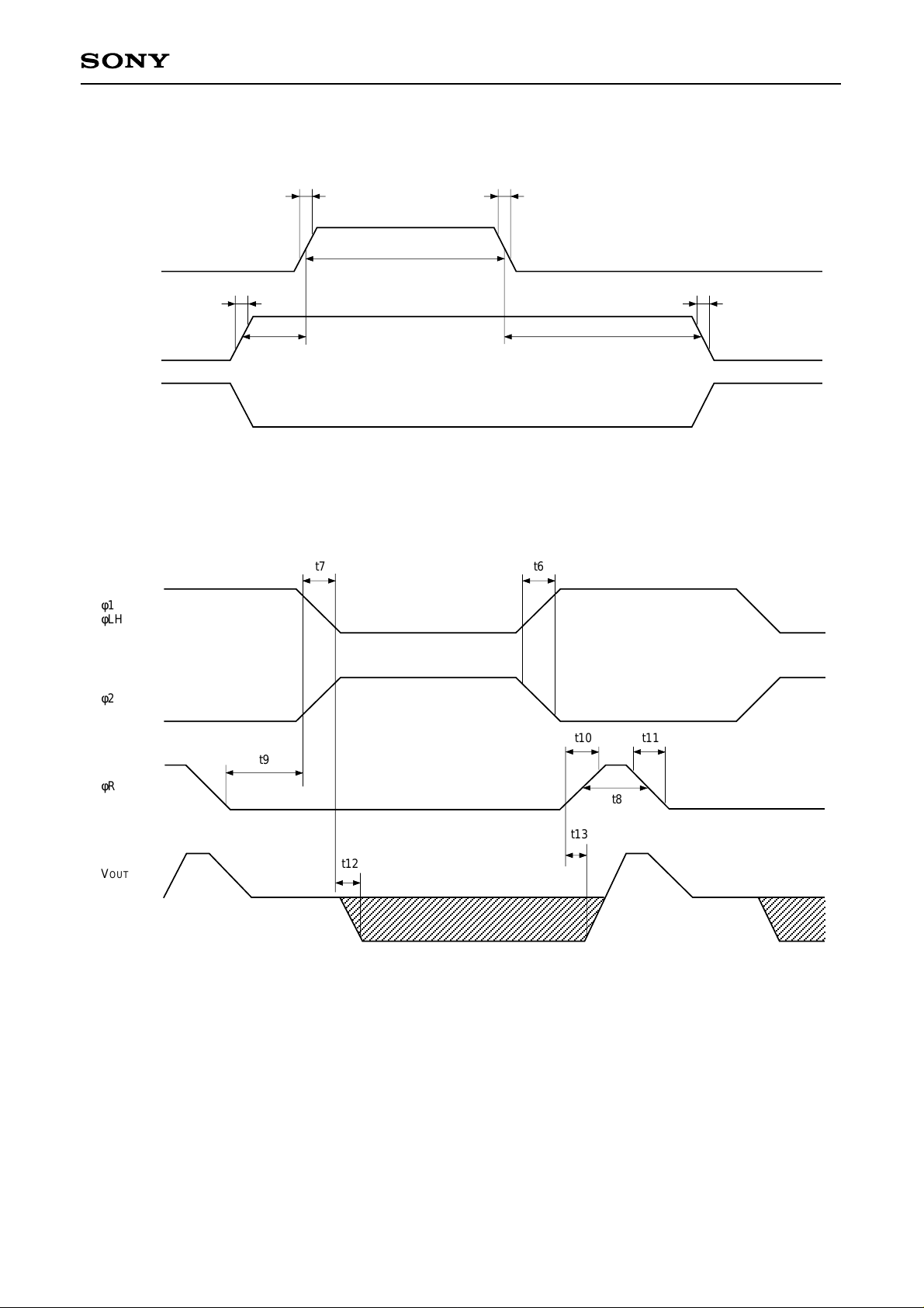
Clock Timing Chart 2
φROG
ILX516K
t4 t5
t2
t7t6
φ1
φ2
Clock Timing Chart 3
φ1
φLH
φ2
φRS
t1 t3
t7
t9
t6
t10 t11
t8
t13
OUT
V
t12
– 5 –
Page 6
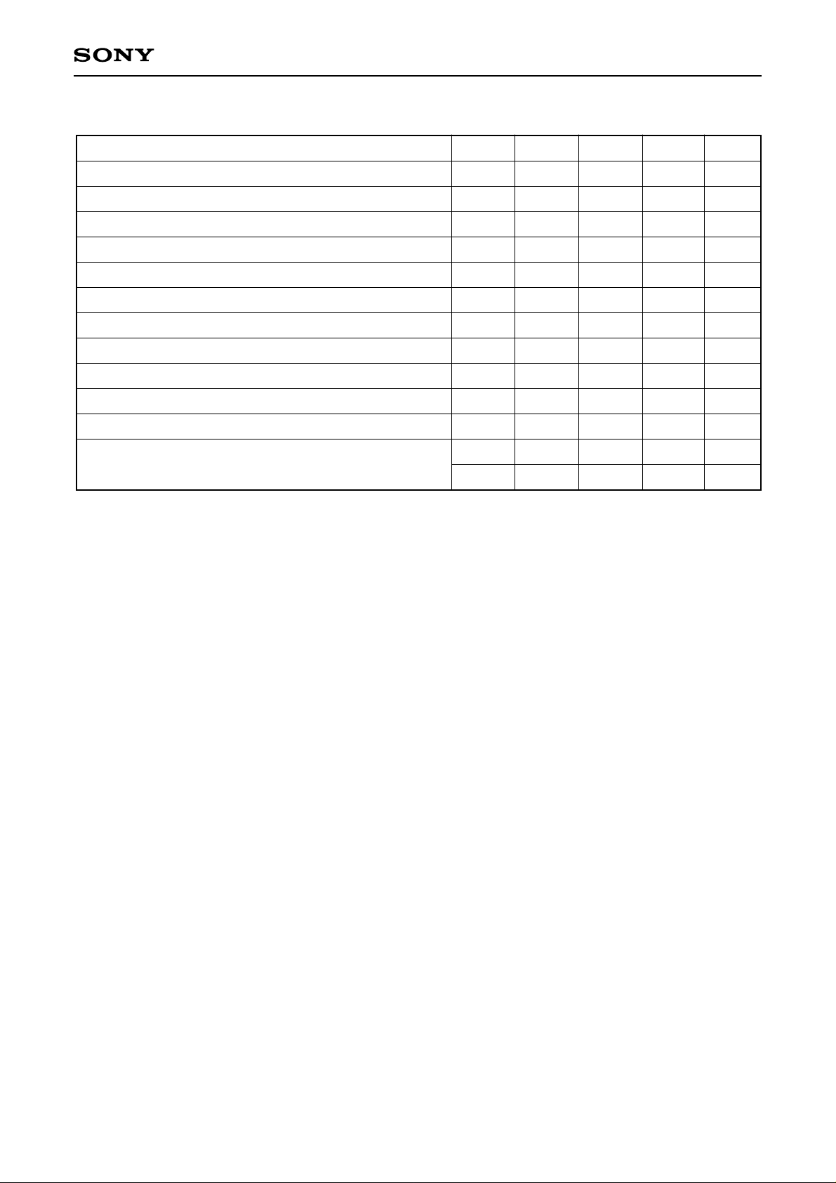
Clock Pulse Recommended Timing
ILX516K
Item
φROG, φ1 pulse timing
φROG pulse high level period
φROG, φ1 pulse timing
φROG pulse rise time
φROG pulse fall time
φ1 pulse rise time /φ2 pulse fall time
φ1 pulse fall time /φ2 pulse rise time
φRS pulse high level period
φRS, φLH pulse timing
φRS pulse rise time
φRS pulse fall time
Signal output delay time
∗
These timing is the recommended condition under fφRS = 1MHz.
Symbol
t1
t2
t3
t4
t5
t6
t7
t8
t9
t10
t11
t12
t13
Min.
50
800
800
0
0
0
0
45
45
0
0
—
—
Typ.
100
1000
1000
5
5
20
20
250
250
10
10
10
10
Max.
—
—
—
10
10
60
60
∗
∗
—
—
30
30
—
—
Unit
ns
ns
ns
ns
ns
ns
ns
ns
ns
ns
ns
ns
ns
– 6 –
Page 7
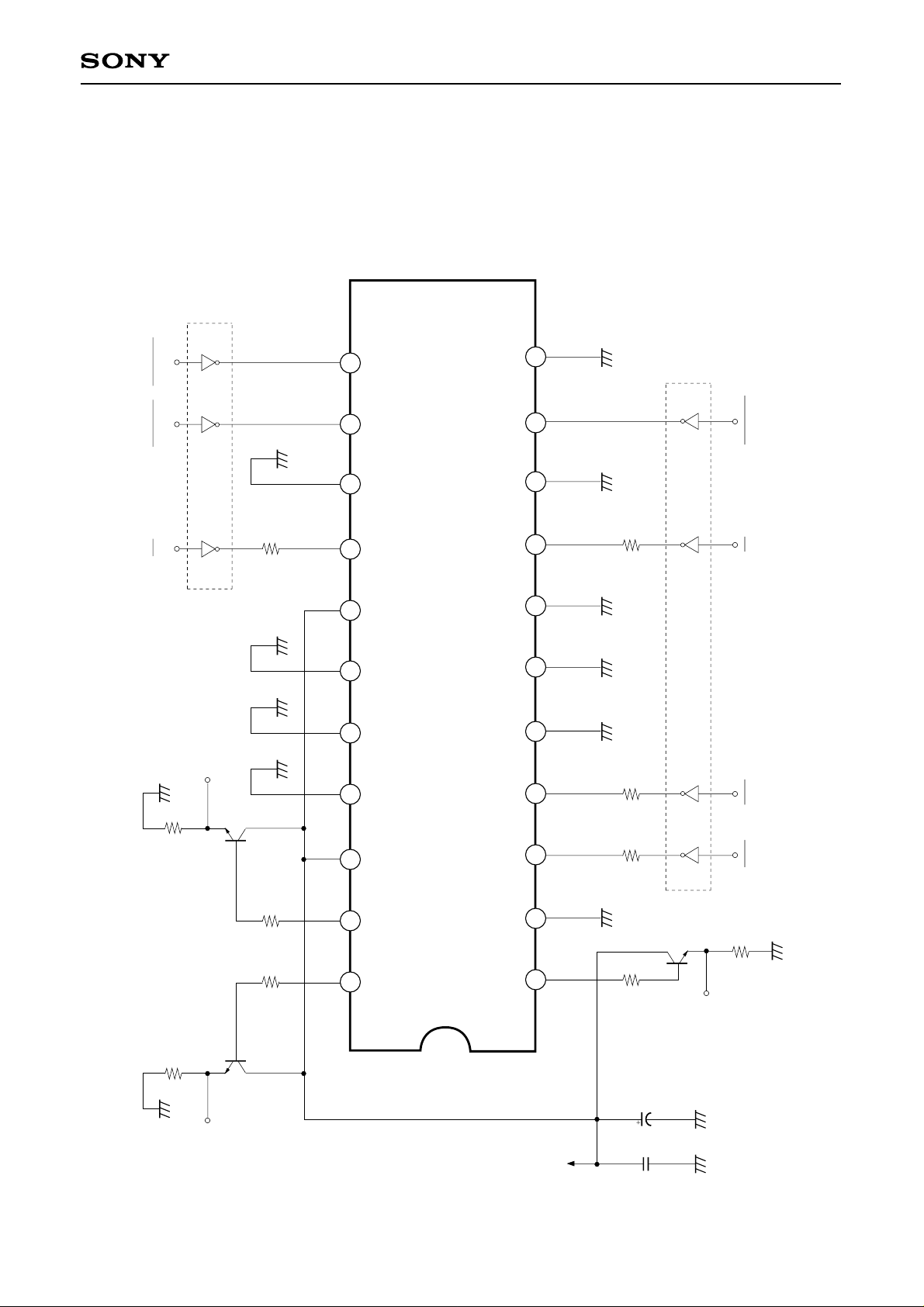
IC1
ILX516K
IC1: 74AC04
Tr1: 2SC2785
φROG
-G
12
φROG
-B
13
NC
1415
φ2 φROG-B φROG-G
φ2
2Ω
V
DD
16
NC
17
NC
18
OUT-B
V
NC
19
Tr1
V
DD
5.1kΩ
20
GND
11
-R
φROG
10
NC
9
φ1
8
IC1
2Ω100Ω
NC
7
NC
6
GND
5
φLH
4
φRS
3
100Ω
Application circuits shown are typical examples illustrating the operation of the devices. Sony cannot assume responsibility for
any problems arising out of the use of these circuits or for any infringement of third party patent and other right due to same.
φRS φLH φ1 φROG-R
5.1kΩ
∗
Application Circuit
VOUT-G
Tr1
100Ω
21
V
OUT-B
GND
2
Tr1
V
V
OUT-G
22
100Ω
OUT-R
1
5.1kΩ
100Ω
OUT-R
V
12V
Data rate fφRS = 1MHz.
0.1µF 47µF/16V
∗
– 7 –
Page 8
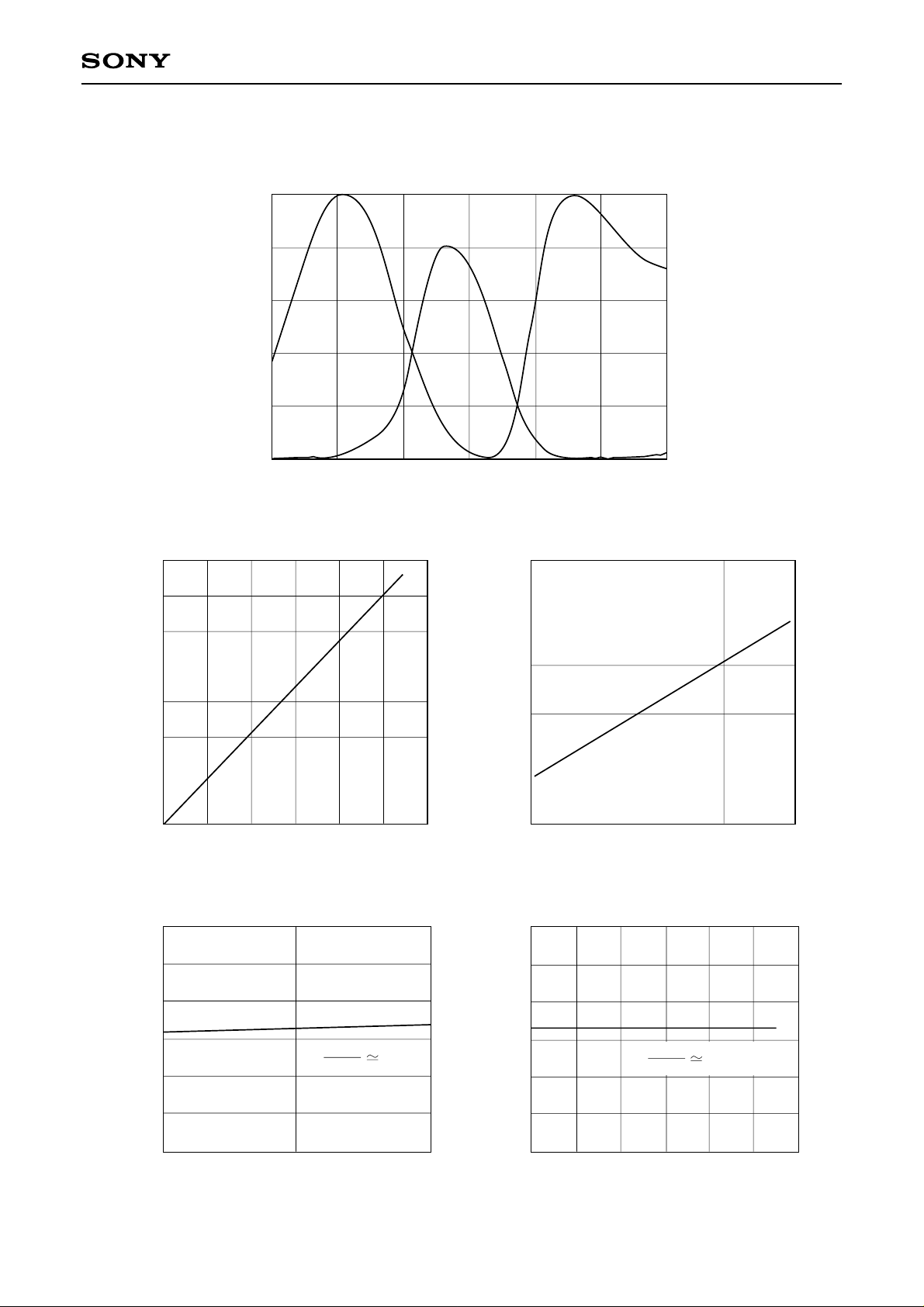
Example of Representative Characteristics (VDD = 12V, Ta = 25°C)
Spectral sensitivity characteristics (Standard characteristics)
1
0.8
0.6
0.4
Relative sensitivity
0.2
0
450400 550500 650600 700
Wavelength [nm]
ILX516K
Dark signal output temperature characteristics
(Standard characteristics)
10
5
1
0.5
Output voltage rate
0.1
0
10 20 30 40 50 60 1
Ta – Ambient temperature [°C]
Offset level vs. VDD characteristics
(Standard characteristics)
12
Ta = 25°C
10
Integration time output voltage characteristics
(Standard characteristics)
1
0.5
Output voltage rate
0.1
510
τint – Integration time [ms]
Offset level vs. temperature characteristics
(Standard characteristics)
12
10
8
6
– Offset level [V]
4
OS
V
2
0
11.4 12.6
V
12
DD [V]
∆V
OS
∆VDD
0.3
– Offset level [V]
OS
V
– 8 –
8
6
4
2
0
0102030405060
Ta – Ambient temperature [°C]
∆VOS
∆Ta
–0.5mV/°C
Page 9
Notes of Handling
1) Static charge prevention
CCD image sensors are easily damaged by static discharge. Before handling be sure to take the following
protective measures.
a) Either handle bare handed or use non chargeable gloves, clothes or material.
Also use conductive shoes.
b) When handling directly use an earth band.
c) Install a conductive mat on the floor or working table to prevent the generation of static electricity.
d) Ionized air is recommended for discharge when handling CCD image sensor.
e) For the shipment of mounted substrates, use boxes treated for prevention of static charges.
2) Notes on Handling CCD Cer-DIP Packages
The following points should be observed when handling and installing cer-DIP packages.
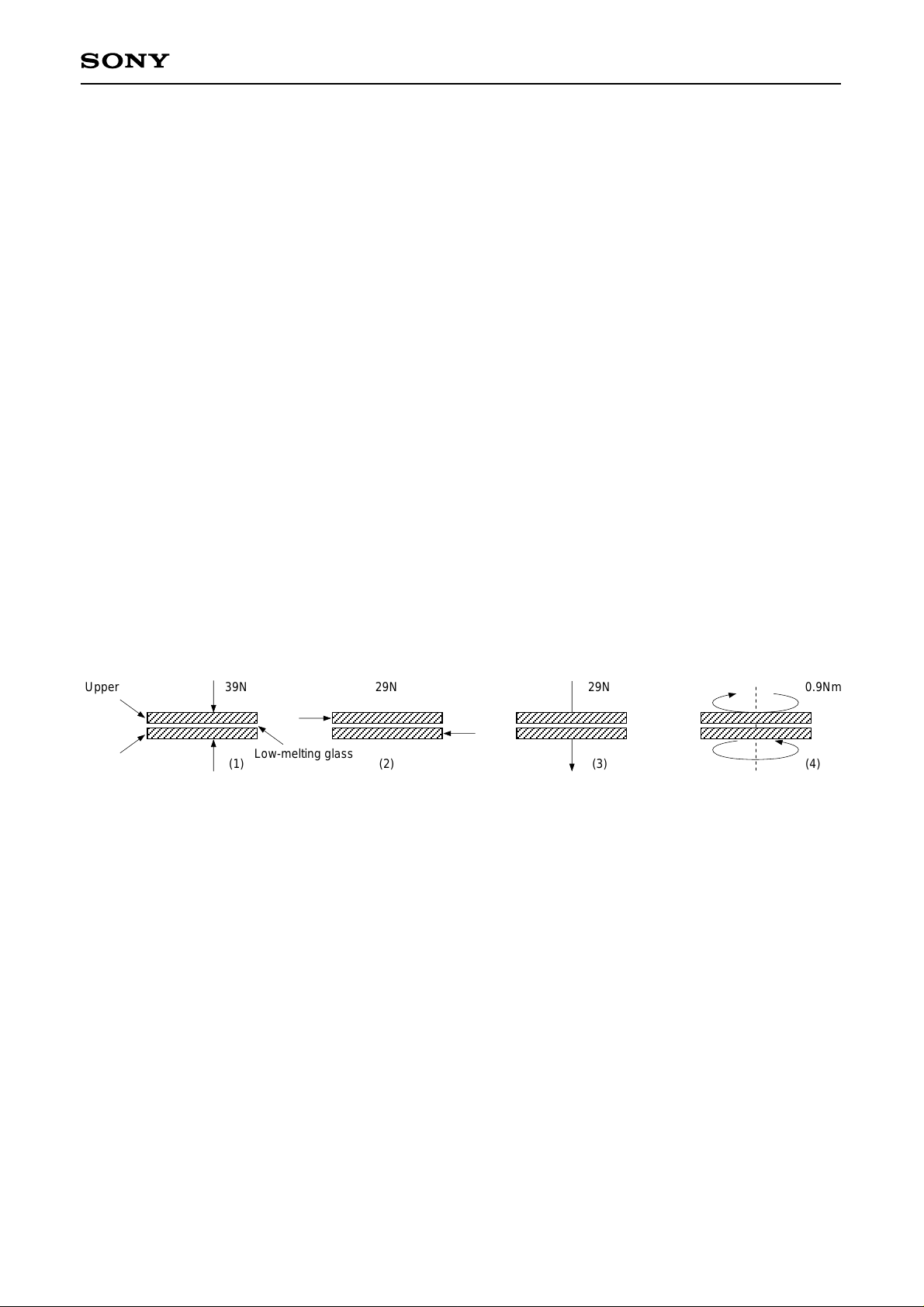
a) Remain within the following limits when applying static load to the ceramic portion of the package:
(1)Compressive strength:39N/surface (Do not apply load more than 0.7mm inside the outer perimeter of
the glass portion.)
(2)Shearing strength: 29N/surface
(3)Tensile strength: 29N/surface
(4)Torsional strength: 0.9Nm
ILX516K
b) In addition, if a load is applied to the entire surface by a hard component, bending stress may be
generated and the package may fracture, etc., depending on the flatness of the ceramic portion.
Therefore, for installation, either use an elastic load, such as a spring plate, or an adhesive.
Upper ceramic layer
lower ceramic layer
39N
Low-melting glass
(1)
29N 29N 0.9Nm
(2) (3) (4)
c) Be aware that any of the following can cause the glass to crack: because the upper and lower ceramic
layers are shielded by low-melting glass,
(1)Applying repetitive bending stress to the external leads.
(2)Applying heat to the external leads for an extended period of time with soldering iron.
(3)Rapid cooling or heating
(4)Rapid cooling or impact to a limited portion of the low-melting glass with a small-tipped tool such as
tweezers.
(5)Prying the upper or lower ceramic layers away at a support point of the low-melting glass.
Note that the preceding notes should also be observed when removing a component from a board after it
has already been soldered.
3) Soldering
a) Make sure the package temperature does not exceed 80°C.
b) Solder dipping in a mounting furnace causes damage to the glass and other defects. Use a grounded 30W
soldering iron and solder each pin in less then 2 seconds. For repairs and remount, cool sufficiently.
c) To dismount an imaging device, do not use a solder suction equipment. When using an electric
desoldering tool, ground the controller. For the control system, use a zero cross type.
– 9 –
Page 10

ILX516K
4) Dust and dirt protection
a) Operate in clean environments.
b) Do not either touch glass plates by hand or have any object come in contact with glass surfaces. Should
dirt stick to a glass surface, blow it off with an air blower. (For dirt stuck through static electricity ionized
air is recommended.)
c) Clean with a cotton bud and ethyl alcohol if the glass surface is grease stained. Be careful not to scratch
the glass.
d) Keep in a case to protect from dust and dirt. To prevent dew condensation, preheat or precool when
moving to a room with great temperature differences.
5) Exposure to high temperatures or humidity will affect the characteristics. Accordingly avoid storage or
usage in such conditions.
6) CCD image sensors are precise optical equipment that should not be subject to mechanical shocks.
– 10 –
Page 11
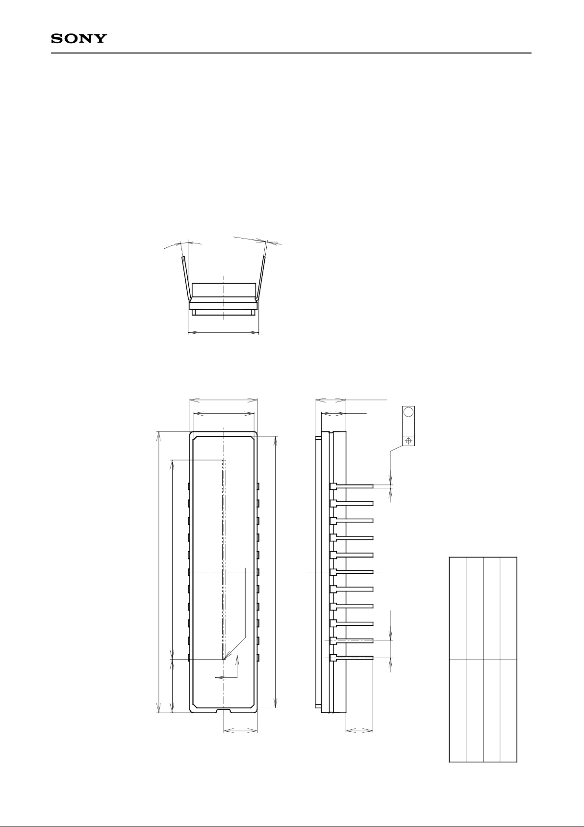
0° to 9°
ILX516K
0.25
12
22pin DIP (400mil)
41.6 ± 0.5
29.184 (8µm × 3648Pixels)
22
7.54 ± 0.8
10.16
(AT STAND OFF)
10.0 ± 0.5
9.0
11
40.2
No.1 Pixel (Green)
1
H
V
1. The height from the bottom to the sensor surface is 2.45 ± 0.3mm.
2. The thickness of the cover glass is 0.8mm, and the refractive index is 1.5.
4.45 ± 0.5
3.65
M
0.3
2.54 0.51
42 ALLOY
TIN PLATING
Cer-DIP
5.2g
Package Outline Unit: mm
5.0 ± 0.54.0 ± 0.5
– 11 –
PACKAGE MATERIAL
LEAD MATERIAL
LEAD TREATMENT
PACKAGE WEIGHT
PACKAGE STRUCTURE
 Loading...