

Page 1
.
.
r
r
r
r
FEATURES
• 7400 Series T2L Compatible
• Transfer Ratio, 35% Typical
• Coupling Capacitance, 0.5 pF
• Single, Dual, & Quad Channel
• Industry Standard DIP Package
• Underwriters Lab File #E52744
V
DE
• VDE Approvals #0884
(Optional with Option 1, Add -X001 Suffix)
DESCRIPTION
The IL74 is an optically coupled pair with a Gallium Arsenide infrared LED and a silicon NPN
phototransistor. Signal information, including a
DC level, can be transmitted by the device while
maintaining a high degree of electrical isolation
between input and output. The IL74 is especially
designed for driving medium-speed logic, where
it may be used to eliminate troublesome gound
loop and noise problems. Also it can be used to
replace relays and transformers in many digital
interface applications, as well as analog applications such as CRT modulation.
The ILD74 has two isolated channels in a single
DIP package; the ILQ74 has four isolated channels per package.
PHOTOTRANSISTOR OPTOCOUPLER
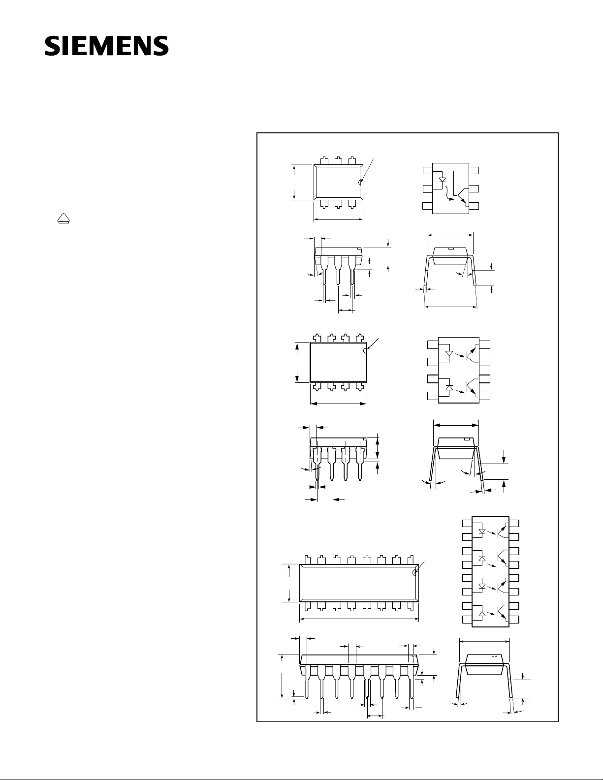
Dimensions in inches (mm)
3
.248 (6.30)
.256 (6.50)
4
5
.335 (8.50)
.343 (8.70)
.039
(1.00)
min.
4°
typ.
.018 (0.45)
.022 (0.55)
2
34
.268 (6.81)
.255 (6.48)
65
.390 (9.91)
.379 (9.63)
.045 (1.14)
.030 (.76)
Pin One ID.
12
6
.130 (3.30)
.150 (3.81)
.020 (.051) min.
.031 (0.80)
.035 (0.90)
.100 (2.54) typ.
Pin One I.D.
1
87
.150 (3.81)
.130 (3.30)
SINGLE CHANNEL
DUAL CHANNEL
QUAD CHANNEL
6
Anode
Cathode
NC
Anode
Cathode
Cathode
Anode
1
2
3
.300 (7.62)
18° typ.
.010 (.25)
.014 (.35)
.300 (7.62)
.347 (8.82)
1
2
3
4
typ.
.305 typ.
(7.75) typ.
Base
5
Collector
4
Emitter
.110 (2.79)
.150 (3.81)
8
7
6
5
IL74
ILD74
ILQ74
Emitter
Collector
Collector
Emitter
4°
Typ.
.022 (.56)
.018 (.46)
67
8
.240 (6.10)
.260 (6.60)
9
10
040 (1.02)
050 (1.27)
.280 (7.11)
.330 (8.38)
.014
(.35)
typ.
.016 (.41)
.020 (.51)
11
.048 (1.22)
.052 (1.32)
.033 (.84)
.040 (1.02)
.030 (.76 )
.100 (2.54) Typ.
5
12
.780 (19.81)
.800 (20.32)
typ.
4
13
3
14
.034 (.86)
3°–9°
1
2
16
15
.100 (2.54) typ.
.020 (.51)
.030 (.76)
Cathode
Cathode
pin one
ID.
Cathode
Cathode
.130 (3.30)
.150 (3.81)
.0255 (.65)
typ.
10°
Typ.
.012 (.30)
.008 (.20)
Anode
Anode
Anode
Anode
1
2
3
4
5
6
7
8
.300 (7.62)
typ.
3° to 9°
.008 (.20)
.012 (.31)
.135 (3.43)
.115 (2.92)
16
15
14
13
12
11
10
9
.130 (3.30)
.150 (3.81)
Emitter
Collecto
Collecto
Emitter
Emitter
Collecto
Collecto
Emitter
5–1
Page 2
:
C
Maximum Ratings
Emitter (each channel)
Peak Reverse Voltage.....................................3.0 V
Continuous Forward Current.........................60 mA
Power Dissipationat 25 °
Derate Linearly from 25 °
C...........................100 mW
C....................1.33 mW/ ° C
Detector (each channel)
Collector-Emitter Breakdown Voltage ..............20 V
Emitter-Base Breakdown Voltage.......................5 V
Collector-Base Breakdown Voltage .................70 V
Power Dissipation at 25 °
Derate Linearly from 25 °
C..........................150 mW
C......................2.0 mW/ ° C
Package
Isolation Test V oltage (t=1 sec.)........5300 VAC
Isolation Resistance
V
=500 V, T
IO
V
=500 V, T
IO
=25 ° C ............................... ≥ 10
A
=100 ° C ............................. ≥ 10
A
RMS
12
11
Ω
Ω
Total Package Dissipation
at 25 °
C Ambient (LED Plus Detector)
IL74.........................................................200 mW
ILD74......................................................400 mW
IL74Q......................................................500 mW
Derate Linearly from 25 °
IL74.....................................................2.7 mW/ °
ILD74................................................5.33 mW/ °
ILQ74................................................6.67 mW/ °
C
C
C
C
Creepage...............................................7 mm min.
Clearance...............................................7 mm min.
Storage Temperature ...................–55 °
Operating Temperature ...............–55 °
Lead Soldering Time at 260 °
Electrical Characteristics (T
Emitter
Forward Voltage V
Reverse Current I
Capacitance C
Detector
Breakdown
Voltage,
Collector-Emitter
Leakage Current,
Collector-Emitter
Capacitance,
Collector-Emitter
Package
DC Current Transfer Ratio
Saturation Voltage,
Collector-Emitter
Resistance, Input
to Output R
Capacitance, Input
to Output C
Switching Times t
C.................... 10 sec.
=25 ° C)
A
Symbol Min. Typ. Max. Unit Condition
F
R
O
BV
CEO
I
CEO
C
CE
CTR
DC
V
CEsat
IO
IO
,t
ON
OFF
C to +150 ° C
C to +100 ° C
1.3 1.5 V I
0.1 100 µ AV
25 pF V
20 50 V I
5.0 500 nA V
10.0 pF V
12.5 35 % I
0.3 0.5
100 G Ω
0.5 pF
3.0
=20 mA
F
=3.0 V
R
=0
R
=1 mA
C
=5 V,
CE
I
=0
F
=0,
CE
F=1 MHz
=16 mA,
F
V
=5 V
CE
I
=2 mA,
C
V
µ sR
=16 mA
I
F
=100 Ω ,
E
V
=10 V,
CE
I
=2 mA
C
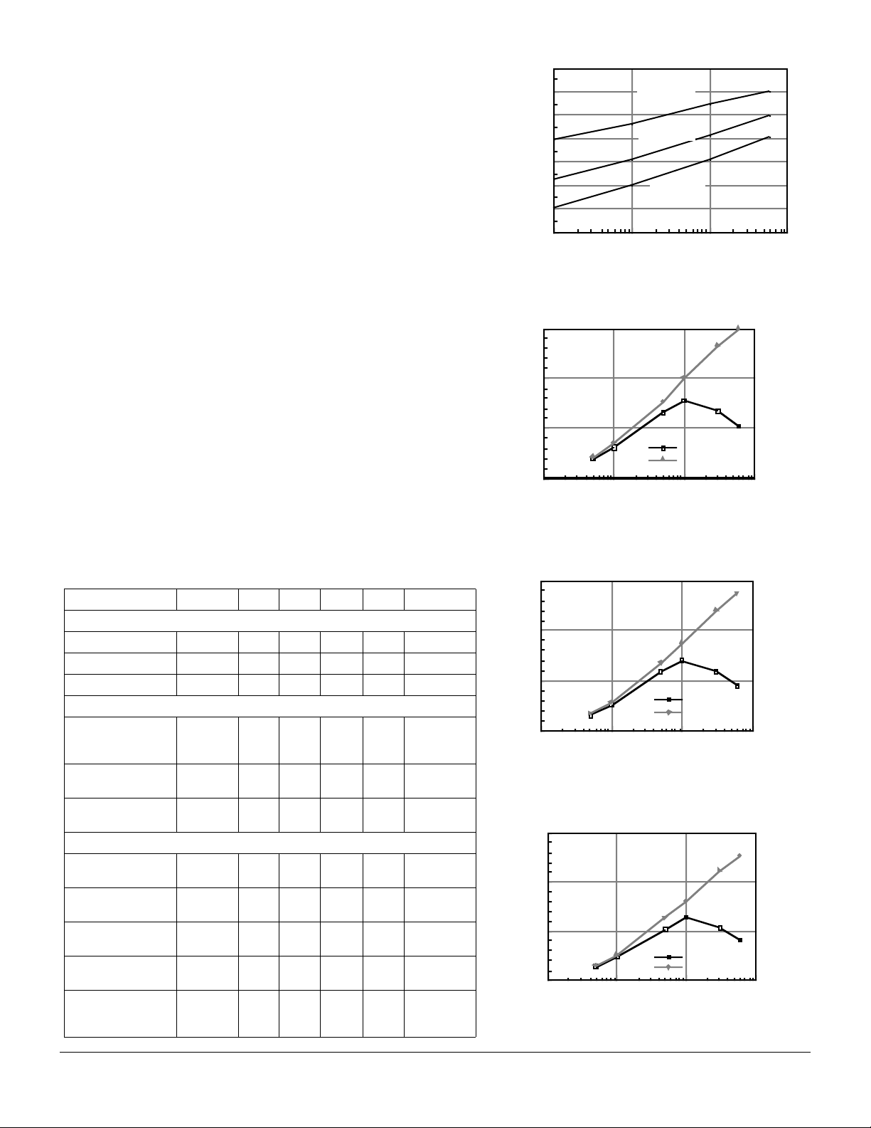
Figure 1. Forward voltage versus forward current
1.4
1.3
Ta = -55°C
1.2
1.1
Ta = 25°C
1.0
0.9
Ta = 85°C
0.8
VF - Forward Voltage - V
0.7
100101.1
IF - Forward Current - mA
Figure 2. Normalized non-saturated and saturated
CTR at T
=25 ° C versus LED current
A
1.5
Normalized to
Vce = 10V, IF = 10mA
Ta = 25°C
1.0
CTRce(sat) Vce = 0.4V
0.5
NCTR - Normalized CTR
0.0
IF - LED Current - mA
NCTR(SAT)
NCTR
100101.1
Figure 3. Normalized non-saturated and saturated
CTR at T
=50 ° C versus LED current
A
1.5
Normalized to:
Vce = 10V, IF = 10mA, Ta = 25°
CTRce(sat) Vce = 0.4V
1.0
Ta = 50°C
0.5
NCTR - Normalized CTR
0.0
IF - LED Current - mA
NCTR(SAT)
NCTR
100101.1
Figure 4. Normalized non-saturated and saturated
CTR at T
=70 ° C versus LED current
A
1.5
Normalized to:
Vce = 10V, IF = 10mA
Ta = 25°C
1.0
CTRce(sat) Vce = 0.4V
0.5
NCTR - Normalized CTR
0.0
IF - LED Current - mA
Ta = 70°C
NCTR(SAT)
NCTR
100101.1
5–2
IL/ILD/ILQ74
Page 3
gp
0
0
C
C
C
C
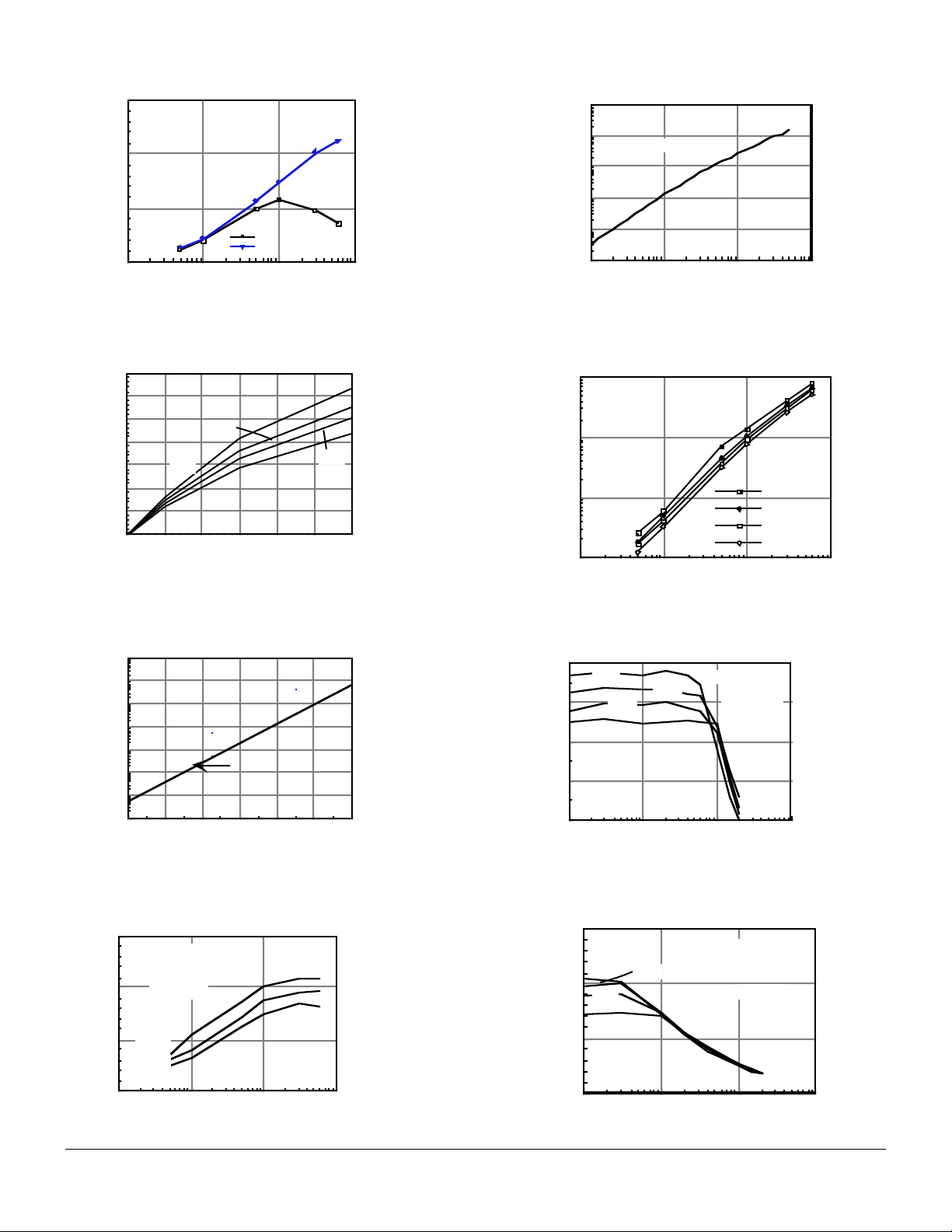
Figure 5. Normalized non-saturated and saturated CTR
at T
=85 ° C versus LED current
A
1.5
Normalized to:
Vce = 10V, IF = 10mA, Ta = 25°C
CTRce(sat) Vce = 0.4V
1.0
0.5
NCTR - Normalized CTR
0.0
IF - LED Current - mA
Ta = 85°C
NCTR(SAT)
NCTR
100101.1
Figure 6. Collector-emitter current ver sus temperature
and LED current
35
30
25
20
15
10
5
0
Ice - Collector Current - mA
50°C
25°C
85°C
IF - LED Current - mA
70°C
6050403020100
Figure 9. Collector base photocurrent versus LED
current
100
Ta = 25°C
10
Icb = 1.0357 *IF ^1.3631
10
1
.1
Photocurrent - µA
Icb - Collector Base
.01
101.1
IF - LED Current - mA
100
Figure 10. Normalized photocurrent versus If and
temperature
10
Normalized Photocurrent
.01
1
.1
Normalized to:
If = 10ma, Ta = 25°C
101.1
NIB-Ta=-20°C
NIb,Ta=25°C
NIb,Ta=50°C
NIb,Ta=70°C
100
Figure 7. Collector-emitter leakage current versus
temperature
5
10
4
10
3
10
2
10
1
10
0
10
-1
10
Iceo - Collector-Emitter - nA
-2
10
Ta - Ambient Temperature - °C
Vce = 10V
TYPICAL
100806040200-20
Figure 8. Normalized CTRcb versus LED current
and temperature
1.5
Normalized to:
IF =10 mA
1.0
0.5
0.0
NCTRcb - Normalized CTRcb
Vcb = 9.3 V
Ta = 25°C
25°C
50°C
70°C
.1 1 10 100
IF - LED Current - mA
Figure 11. Normalized non-saturated HFE versus
base current and temperature
1.2
70°C Normalized to:
1.0
-20°C
0.8
0.6
NHFE - Normalized HFE
0.4
1 10 100 1000
50°C
25°C
Ib - Base Current - µA
Ib = 20µA
Vce = 10 V
Ta = 25°C
Figure 12. Normalized saturated HFE versus base
current and temperature
1.5
70°
1.0
50°
25°C
-20°
0.5
Saturated HFE
Vce = 0.4V
NHFE(sat) - Normalized
0.0
1 10 100 1000
Ib - Base Current - (µA)
Normalized to:
Vce = 10V
Ib = 20µA
Ta = 25°
5–3
IL/ILD/ILQ74
Page 4
A
V
A
V
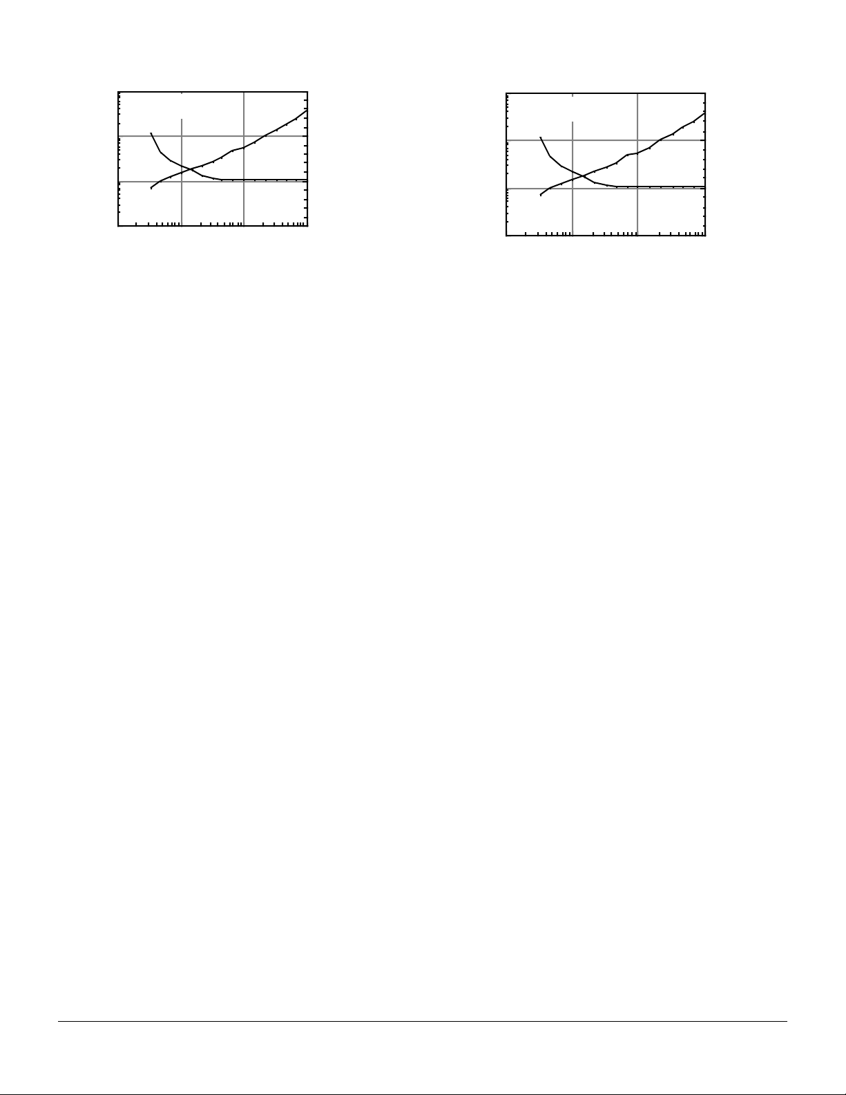
Figure 13. Propagation delay versus collector load resistor
1000
tpLH - Propagation Delay - µs
Ta = 25°C, IF = 10m
Vcc = 5 V, Vth = 1.5
100
10
1
tpHL
tpLH
RL - Collector Load Resistor - KΩ
2.5
2.0
1.5
tpHL - Propagation Delay - µs
1.0
100101.1
Figure 14. Propagation delay versus collector load resistor
1000
tpLH - Propagation Delay - µs
Ta = 25°C, IF = 10m
Vcc = 5 V, Vth = 1.5
tpHL
100
10
tpLH
1
RL - Collector Load Resistor - KΩ
2.5
2.0
1.5
tpHL - Propagation Delay - µs
1.0
100101.1
5–4
IL/ILD/ILQ74
 Loading...