

Page 1

2048-pixel CCD Linear Image Sensor (B/W)
For the availability of this product, please contact the sales office.
Description
The ILX503A is a reduction type CCD linear sensor
designed for facsimile, image scanner and OCR use.
This sensor reads B4 size documents at a density of
200 DPI (Dot Per Inch). A built-in timing generator
and clock-drivers ensure direct drive at 5V logic for
easy use.
Features
• Number of effective pixels: 2048 pixels
• Pixel size: 14µm × 14µm (14µm pitch)
• Built-in timing generator and clock-drivers
• Ultra low lag
• Maximum clock frequency: 5MHz
Absolute Maximum Ratings
• Supply voltage VDD1 11 V
VDD2 6V
•Operating temperature –10 to +55 °C
• Storage temperature –30 to +80 °C
ILX503A
22 pin DIP (Plastic)
Pin Configuration (Top View)
OUT
V
1
GND
2
GND
3
SHSW
φROG
Sony reserves the right to change products and specifications without prior notice. This information does not convey any license by
any implication or otherwise under any patents or other right. Application circuits shown, if any, are typical examples illustrating the
operation of the devices. Sony cannot assume responsibility for any problems arising out of the use of these circuits.
φCLK
DD1
V
GND
DD2
V
T1
NC
4
5
6
7
8
9
10
11
1
2048
22
21
20
19
18
17
16
15
14
13
12
DD2
V
EXRS
VDD1
RSSW
VGG
GND
GND
VDD1
NC
NC
GND
– 1 –
E92Y21E78-PS
Page 2

10
ILX503A
NC
DD1
DD1
GND
NC
NC
V
GND
GND
V
12
13
1415
16
17
20
D39
D38
D37
D36
D35
D34
S2048
S2047
S2
S1
D33
D15
D14
Read out gate
CCD analog shift register
Clock-drivers
Read out gate
pulse generator
Mode
selector
11
4
21
19
5
9
φROG
SHSW
EXRS
RSSW
φCLK
T1
Block Diagram
DD2
V
DD2
V
22
Output amplifier
Sample-and-hold
circuit
1
VOUT
18
VGG
Clock pulse generator
Sample-and-hold pulse
generator
8
GND
7
V
DD1
6
GND
3
GND
2
– 2 –
Page 3

Pin Description
ILX503A
Pin No.
1
2
3
4
5
6
7
8
9
10
11
12
13
14
15
Symbol
VOUT
GND
GND
SHSW
φCLK
VDD1
GND
VDD2
T1
NC
φROG
GND
NC
NC
VDD1
Signal output
GND
GND
Switch
Clock pulse
9V power supply
GND
5V power supply
Test pin (VDD2)
Clock pulse
GND
9V power supply
with S/H → GND
{
without S/H → VDD2
Description
16
17
18
19
20
21
22
GND
GND
VGG
RSSW
VDD1
EXRS
VDD2
GND
GND
Output circuit gate bias
RS pulse external, internal selection
(External RS → VDD2, Internal RS → GND)
9V power supply
RS input pin during external RS pulse usage
5V power supply
– 3 –
Page 4

Recommended Voltage
ILX503A
Item
VDD1
VDD2
Min.
8.5
4.75
Typ.
9.0
5.0
Max.
9.5
5.25
Unit
V
V
Note) Rules for raising and lowering power supply voltage
To raise power supply voltage, first raise VDD1(9V) and then VDD2 (5V).
To lower voltage, first lower VDD2 (5V) and then VDD1 (9V).
Mode Description
Mode Description Pin condition
21 pin EXRS
Yes
4 pin SHSWS/HRS
GND
19 pin RSSW
GND
Internal
GND
VDD2
Externel
No
No
VDD2
VDD2
Input Capacity of Pins
VDD2
VDD2
φRS
Item
Input capacity of φCLK pin
Input capacity of φROG pin
Input capacity of EXRS pin
Symbol
CφCLK
CφROG
CEXRS
Recommended Input Pulse Voltage
Parameter
Input clock high level
Input clock low level
Min.
4.5
0.0
Typ.
5.0
—
Min.
—
—
—
Max.
5.5
0.5
Typ.
10
10
10
Unit
Max.
—
—
—
Unit
pF
pF
pF
V
V
– 4 –
Page 5
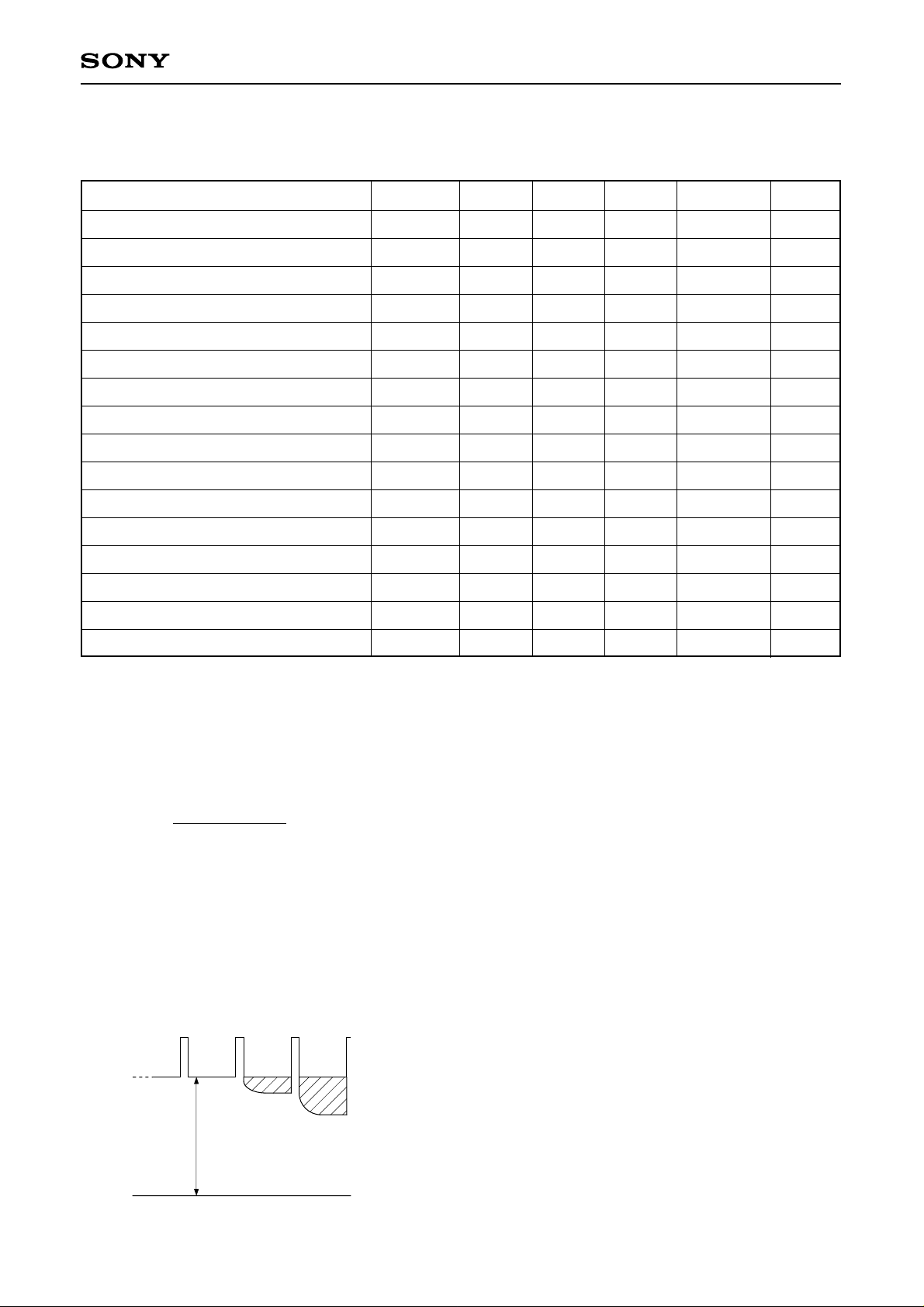
Electro-optical Characteristics
ILX503A
(Ta = 25°C, VDD1 = 9V, VDD2 = 5V, Clock frequency: 1MHz,
Light source = 3200K, IR cut filter: CM-500S (t = 1.0mm)),
When Internal RS (Pin 19 = GND, Pin 21 = VDD2)
Item
Sensitivity 1
Sensitivity 2
Sensitivity 3
Sensitivity 4
Sensitivity nonuniformity
Saturation output voltage
Dark voltage average
Dark signal nonuniformity
Image lag
Dynamic range
Saturation exposure
9V supply current
5V supply current
Total transfer efficiency
Output impedance
Offset level
Symbol
R1
R2
R3
R4
PRNU
VSAT
VDRK
DSNU
IL
DR
SE
IVDD1
IVDD2
TTE
ZO
VOS
Min.
22.5
—
—
—
—
1.5
—
—
—
750
0.040
—
—
92.0
—
—
Typ.
30
95
20
500
2.0
1.8
0.3
0.5
0.02
6000
0.060
8.0
3.0
97.0
600
4.5
Max.
37.5
—
—
—
8.0
—
2.0
3.0
—
—
—
14.0
6.0
—
—
—
Unit
V/(lx · s)
V/(lx · s)
V/(lx · s)
V/(lx · s)
mV
mV
lx · s
mA
mA
Notes)
1) For the sensitivity test light is applied with a uniform intensity of illumination.
2) W lamp (2854K)
3) Light source: LED λ = 570nm
4) Light source: LED λ = 660nm
5) PRNU is defined as indicated below. Ray incidence conditions are the same as for Note 1.
%
V
%
—
%
Ω
V
Remarks
Note 1
Note 2
Note 3
Note 4
Note 5
—
Note 6
Note 6
Note 7
Note 8
Note 9
—
—
—
—
Note 10
PRNU = × 100 [%]
(VMAX – VMIN)/2
VAVE
The maximum output is set to VMAX, the minimum output to VMIN and the average output to VAVE.
6) Integration time is 10ms.
7) VOUT = 500mV
8) DR = VSAT/VDRK
When optical accumulated time is shorter, the dynamic range gets wider because dark voltage is in
propagation to optical accumulated time.
9) SE = VSAT/R1
10) VOS is defined as indicated below.
D32 D33 S1D31
OS
OS
V
– 5 –
GND
Page 6
ILX503A
2
1
DD2)
2087
D39
D38
D37
D36
D35
D34
S2048
S2047
S2046
S2045
S4
S3
S2
S1
D33
D32
D31
D15
D14
D13
D12
D11
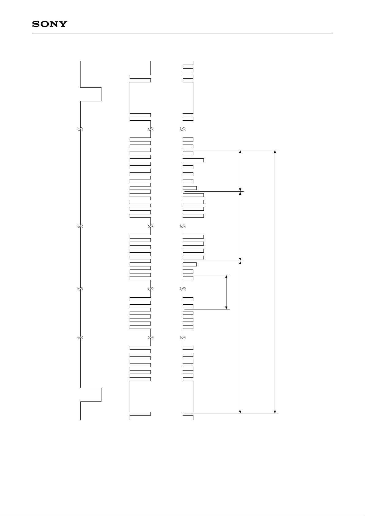
Dummy signal
(6 pixels)
Effective picture
elements signal
(2048 pixels)
Optical black
(18 pixels)
Internal S/H is not in use (Pin 4 → V
∗
1-line output period (2087 pixels)
5
φROG
Clock Timing Diagram (For internal RS mode)
D6
D5
4
3
2
1
0
5
0
φCLK
D4
D3
D2
D1
∗
OUT
V
Dummy signal (33 pixels)
– 6 –
Page 7
ILX503A
2
1
2087
D39
D38
D37
D36
D35
D34
S2048
S2047
S2046
S2045
S4
S3
S2
S1
D33
D32
D31
D15
D14
D13
D12
D11
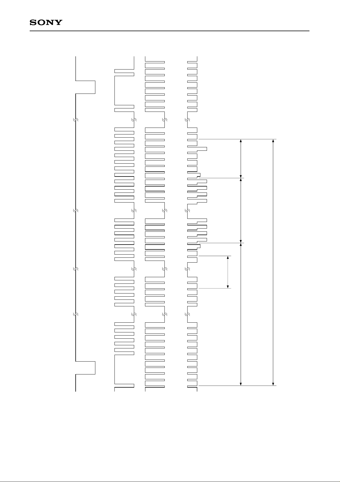
Dummy signal
(6 pixels)
Effective picture
elements signal
(2048 pixels)
Optical black
(18 pixels)
1-line output period (2087 pixels)
5
φROG
Clock Timing Diagram (For external RS mode)
D6
D5
4
3
2
1
0
5
φCLK
0
5
0
φRS
D4
D3
D2
OUT
V
Dummy signal (33 pixels)
– 7 –
Page 8
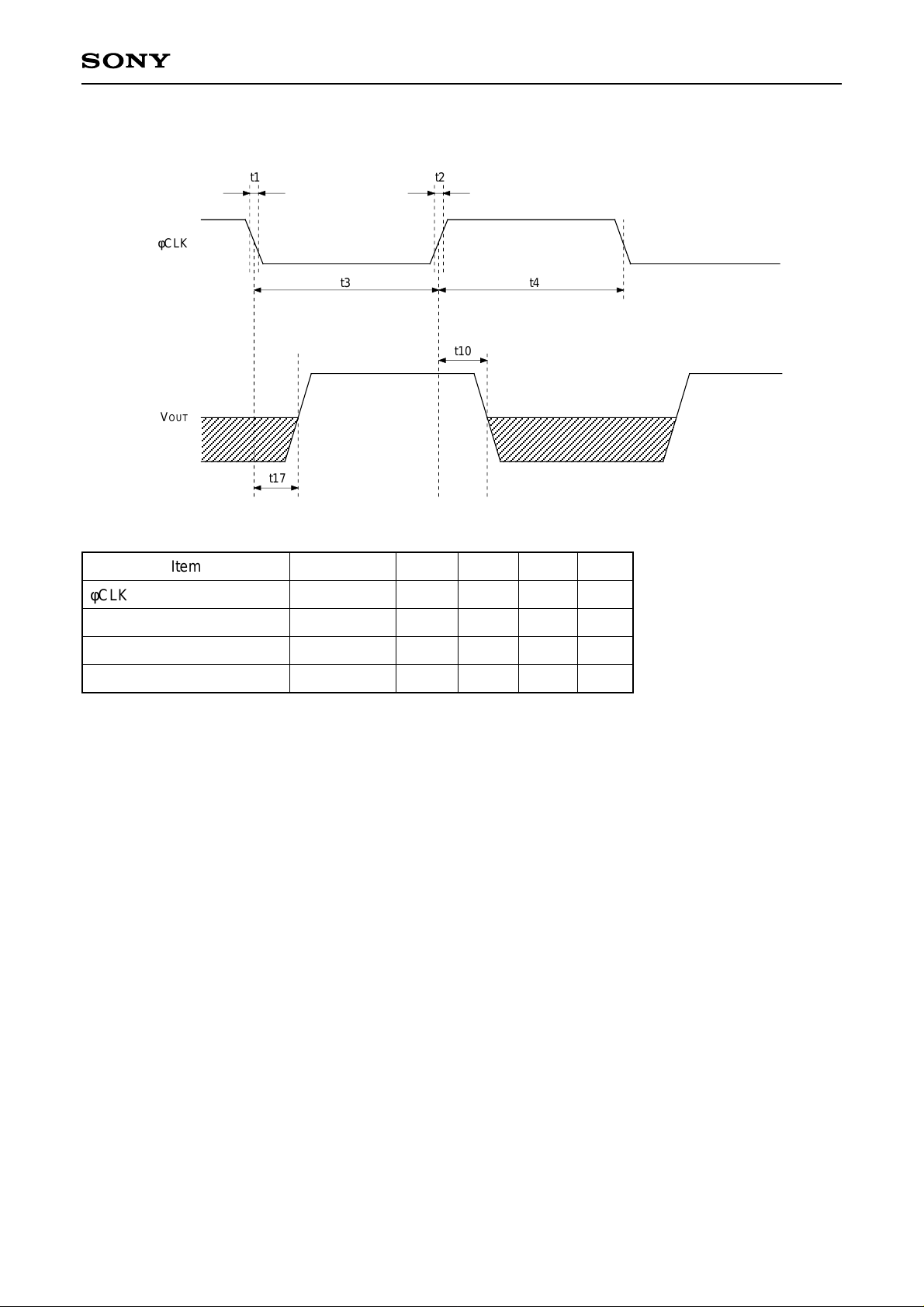
φCLK, VOUT Timing (For internal RS mode)
t1 t2
φCLK
t3 t4
VOUT
t17
ILX503A
t10
Item
φCLK pulse rise/fall time
φCLK pulse duty
∗1
φCLK – VOUT 1
φCLK – VOUT 2
∗1
100 × t3/(t3 + t4)
Symbol
t1, t2
t10
t17
—
Min.
0
40
50
30
Typ.
10
50
80
75
Max.
—
60
110
120
Unit
ns
%
ns
ns
– 8 –
Page 9
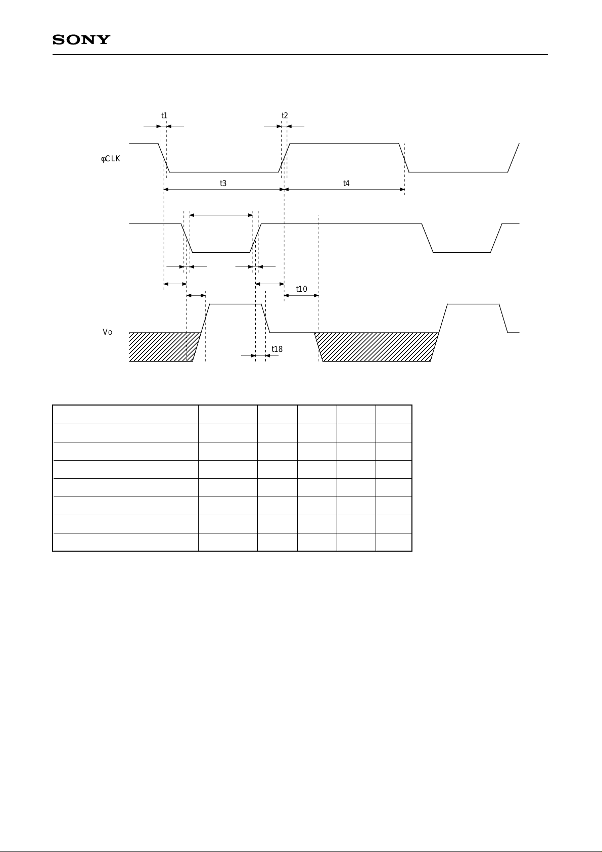
φCLK, φRS, VOUT Timing (For external RS mode)
t1 t2
φCLK
t3 t4
t5
φRS
t8 t9
t11
VOUT
ILX503A
t7t6
t10
Item
φCLK, φRS pulse rise/fall time
φCLK pulse duty
∗1
φCLK – φRS pulse timing
φCLK – φRS pulse timing
φRS pulse period
φCLK – VOUT
φRS – VOUT
∗1
100 × t3/(t3 + t4)
Symbol
t1, t2, t8, t9
—
t6
t7
t5
t10
t11, t18
t18
Min.
—
40
0
50
50
50
30
Typ.
10
50
100
100
100
80
50
Max.
50
60
—
—
—
110
70
Unit
ns
%
ns
ns
ns
ns
ns
– 9 –
Page 10
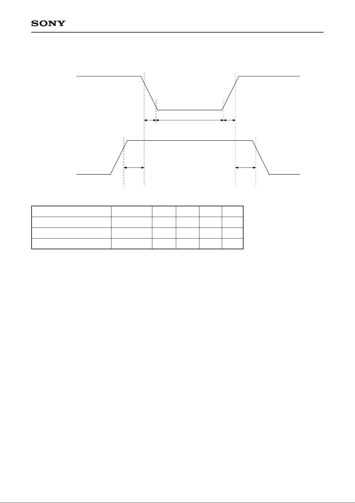
φROG, φCLK Timing
φROG
φCLK
t12
ILX503A
t15t13 t14
t16
Item
φROG, φCLK pulse timing
φROG pulse rise/fall time
φROG pulse period
Symbol
t12, t16
t13, t15
t14
Min.
500
0
500
Typ.
1000
10
1000
Max.
—
—
—
Unit
ns
ns
ns
– 10 –
Page 11
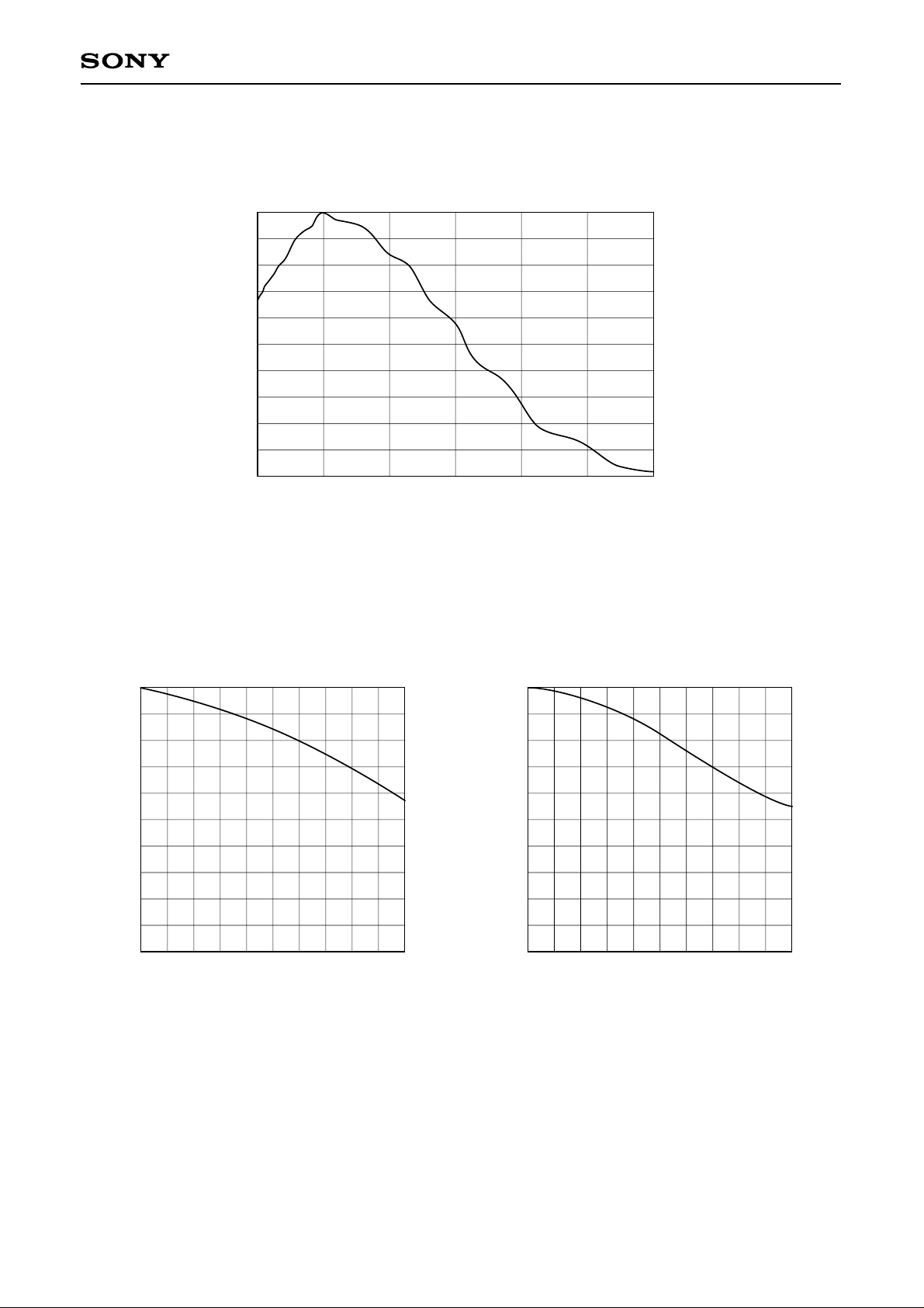
Example of Representative Characteristics
Spectral sensitivity characteristics
(Standard characteristics)
1.0
0.9
0.8
0.7
0.6
0.5
0.4
Relative sensitivity
0.3
0.2
0.1
0
400 500 600 700 800 900 1000
ILX503A
Ta = 25°C
Wavelength [nm]
1.0
0.8
0.6
X-MTF
0.4
0.2
MTF of main scanning direction
(Standard characteristics)
Spatial frequency [cycles/mm]
0
0
0
7.1 14.3 21.4 28.6 35.7
0.2 0.4 0.6 0.8 1.0
Normalized spatial frequency
1.0
0.8
0.6
Y-MTF
0.4
0.2
0
MTF of sub scanning direction
(Standard characteristics)
Spatial frequency [cycles/mm]
0
0
7.1 14.3 21.4 28.6 35.7
0.2 0.4 0.6 0.8 1.0
Normalized spatial frequency
– 11 –
Page 12
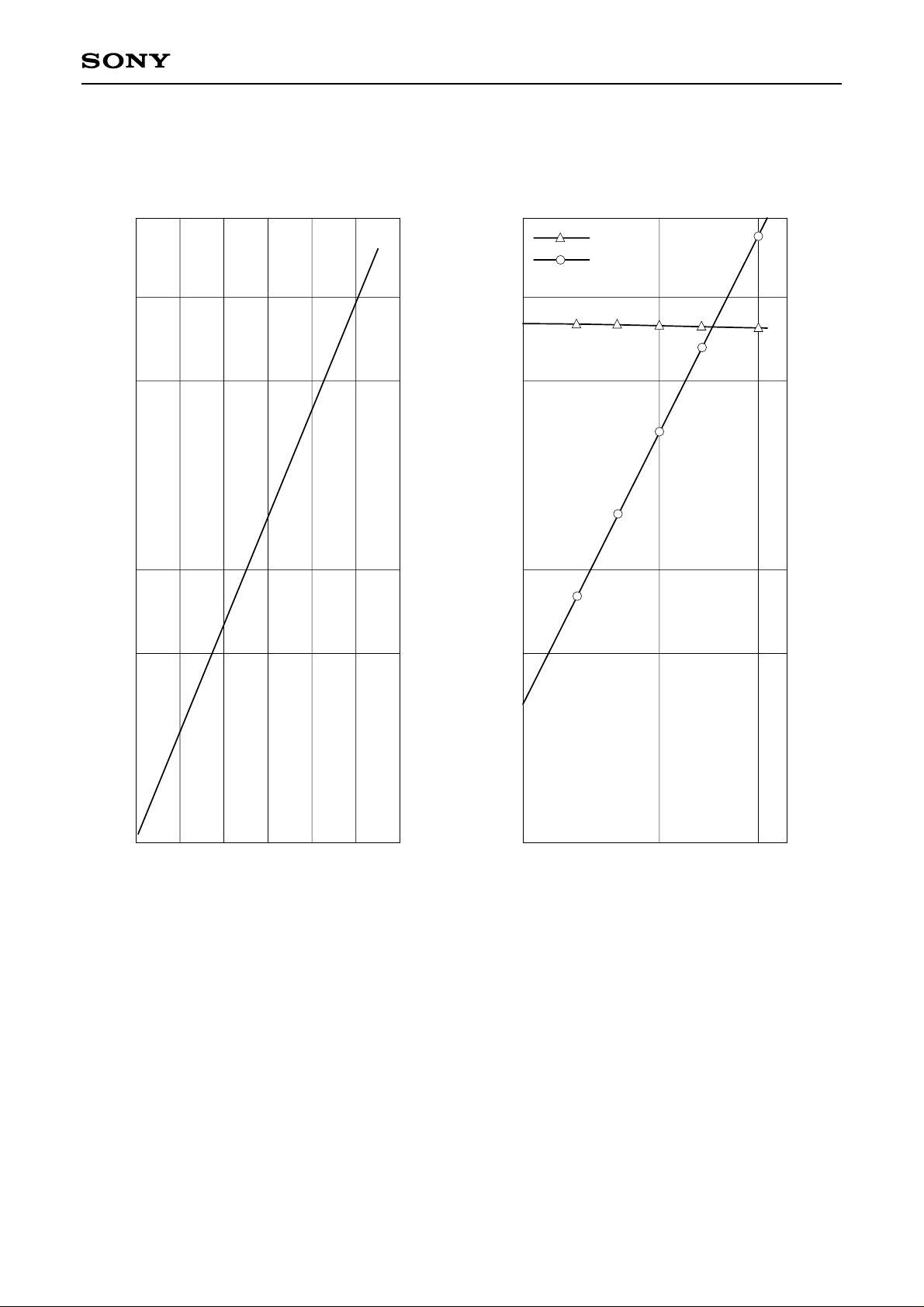
ILX503A
Dark signal voltage rate vs. Ambient temperature
(Standard characteristics)
10
5
1
Dark signal voltage rate
0.5
VDD1, VDD2 supply current vs. Clock frequency
(Standard characteristics)
IVDD1
IVDD2
10
5
supply current [mA]
DD2
, V
DD1
1
– V
VDD2
, I
VDD1
I
0.5
0.1
0
10 20 30 40 50
Ta – Ambient temperature [°C]
– 12 –
0.1
0.1M
1M 5M
Clock frequency [Hz]
Page 13
1222 21 20 19 18 17 16 15 14 13
ILX503A
22µ/10V0.01µ
(D)
φROG
NC GND
10µ/16V
NC
(A)
VDD1
(A)
GND
(A)
RSSW VGG GND
(A)
EXRS VDD1
(D)
VDD2
22 pin DIP
(D)
(D)
(A)
(A)
(D)
T1 NC
VDD2
GND
VDD1
φCLK
SHSW
GND
GND
1 2 3 4 5 6 7 8 9 10 11
VOUT
φCLK φROG
2SA1175
Application circuits shown are typical examples illustrating the operation of the devices. Sony cannot assume responsibility for
any problems arising out of the use of these circuits or for any infringement of third party patent and other right due to same.
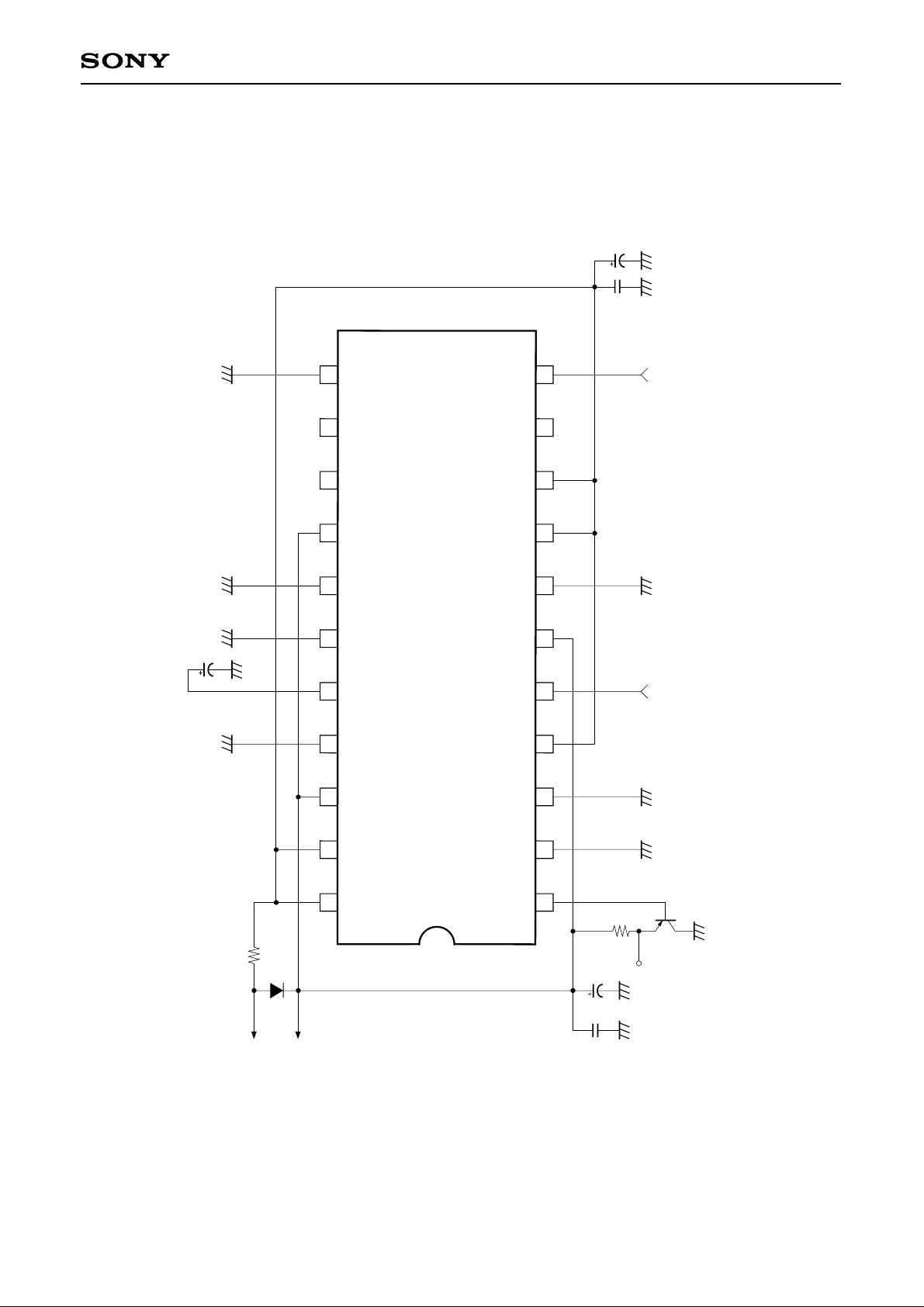
Application Circuit (When internal RS)
1Ω
5V
9V
3kΩ
10µ/16V0.01µ
Output signal
– 13 –
Page 14

Notes on Handling
1) Static charge prevention
CCD image sensors are easily damaged by static discharge. Before handling be sure to take the following
protective measures.
a) Either handle bare handed or use non chargeable gloves, clothes or material. Also use conductive shoes.
b) When handling directly use an earth band.
c) Install a conductive mat on the floor or working table to prevent the generation of static electricity.
d) Ionized air is recommended for discharge when handling CCD image sensor.
e) For the shipment of mounted substrates, use boxes treated for the prevention of static charges.
2) Regulation for raising and lowering the power supply voltage
When raising the supply voltage, first raise VDD1 (9V) and then VDD2 (5V). Similarly, lower VDD2 (5V) first and
then VDD1 (9V).
3) Soldering
a) Make sure the package temperature does not exceed 80°C.
b) Solder dipping in a mounting furnace causes damage to the glass and other defects. Use a grounded 30W
soldering iron and solder each pin in less than 2 seconds. For repairs and remount, cool sufficiently.
c) To dismount an image sensor, do not use a solder suction equipment. When using an electric desoldering
tool, ground the controller. For the control system, use a zero cross type.
ILX503A
4) Dust and dirt protection
a) Operate in clean environments.
b) Do not either touch glass plates by hand or have any object come in contact with glass surfaces. Should
dirt stick to a glass surface, blow it off with an air blower. (For dirt stuck through static electricity ionized air
is recommended.)
c) Clean with a cotton bud and ethyl alcohol if the grease stained. Be careful not to scratch the glass.
d) Keep in a case to protect from dust and dirt. To prevent dew condensation, preheat or precool when
moving to a room with great temperature differences.
5) Exposure to high temperatures or humidity will affect the characteristics. Accordingly avoid storage or
usage in such conditions.
6) CCD image sensors are precise optical equipment that should not be subject to mechanical shocks.
– 14 –
Page 15
0° to 9°
0.25
10.16
(AT STAND OFF)
10.0 ± 0.5
9.0
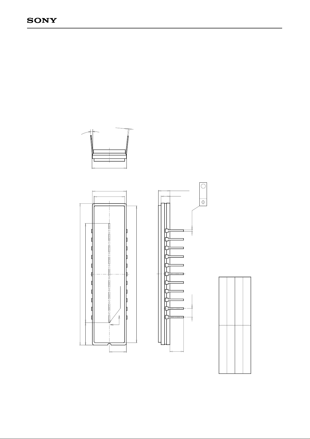
1. The height from the bottom to the sensor surface is 1.61 ± 0.3mm.
2. The thickness of the cover glass is 0.7mm, and the refractive
index is 1.5 .
3.3 ± 0.5
2.6
M
0.3
ILX503A
12
22pin DIP (400mil)
41.6 ± 0.5
28.672 (14µm × 2048Pixels)
22
7.35 ± 0.8
40.2
No.1 Pixel
111
H
V
5.0 ± 0.5
4.0 ± 0.5
0.51
2.54
Cer-DIP
PACKAGE MATERIAL
PACKAGE STRUCTURE
42 ALLOY
TIN PLATING
LEAD TREATMENT
3.9g
PACKAGE WEIGHT
LEAD MATERIAL
Package Outline Unit: mm
– 15 –
 Loading...